III-V epitaxy MOCVD MBE substrate & equipment market - I-Micronews
III-V epitaxy MOCVD MBE substrate & equipment market - I-Micronews
III-V epitaxy MOCVD MBE substrate & equipment market - I-Micronews
You also want an ePaper? Increase the reach of your titles
YUMPU automatically turns print PDFs into web optimized ePapers that Google loves.
Aixtron<br />
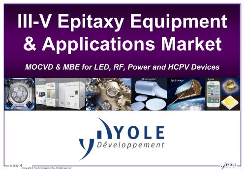
<strong>III</strong>-V Epitaxy Equipment<br />
& Applications Market<br />
<strong>MOCVD</strong> & <strong>MBE</strong> for LED, RF, Power and HCPV Devices<br />
Veeco<br />
Growing<br />
Chemical-mechanical<br />
→<br />
→<br />
© 2012• 1 Copyrights © Yole Développement SA. All rights reserved.<br />
Core Fabrication<br />
Geometry inspection<br />
Monocrystal<br />
Riber Spot Image<br />
→<br />
→<br />
Wafer Slicing<br />
Optical inspection<br />
→<br />
→<br />
Apple<br />
Lapping<br />
Final cleaning<br />
→<br />
→<br />
D<br />
E
© 2012• 2 Copyrights © Yole Développement SA. All rights reserved.<br />
Report Scope<br />
This report covers the following <strong>III</strong>-V semiconductor applications:<br />
Applications Components Materials Main Substrates<br />
High Brightness LEDs<br />
High Brightness LEDs<br />
RF Electronic<br />
High Concentrated Photo-Voltaic<br />
Power GaN<br />
Blue, Green and white<br />
(with phosphor) LEDs<br />
GaN, InGaN,<br />
InAlGaN<br />
Red-Yellow-Orange LEDs InGaAlP • GaAs<br />
Power amplifiers<br />
Antenna switches<br />
(Technologies: HBT, HEMT,<br />
FET)<br />
AlGaAs,<br />
InGaAs,<br />
InGaP,<br />
GaAsInN<br />
Photovoltaic cells GaAs, AlGaAs,<br />
GaInAs, GaInP<br />
AlGaInP,<br />
AlInAs,<br />
GaInNAsSb<br />
Inverters, converters (DC-<br />
DC, AC-DC, DC-AC), RF<br />
Transistors.<br />
(Technologies: HEMT,<br />
HBT)<br />
Report Scope<br />
GaN, InGaN,<br />
AlGaN<br />
• Sapphire<br />
• SiC<br />
• Silicon (emerging)<br />
• GaN (Emerging)<br />
• GaAs<br />
• Germanium<br />
• GaAs (Emerging)<br />
• Silicon<br />
(mainstream)<br />
• Sapphire<br />
• SiC
© 2012• 3 Copyrights © Yole Développement SA. All rights reserved.<br />
<strong>MBE</strong> (2)<br />
• <strong>MBE</strong> <strong>market</strong> is driven by the steady growth in cell phone and wireless devices.<br />
However, the opportunity will be somehow be limited by advances in <strong>MOCVD</strong> that<br />
will be used to manufacture an increasing number of GaAs HBT and HEMT.<br />
• HCPV will provide a small potential upside for <strong>MBE</strong> as well.<br />
March 2012<br />
Executive Summary
H 2<br />
N 2<br />
Purifier<br />
Purifier<br />
V-hydride<br />
precursor V-hydride<br />
precursor<br />
Dopant<br />
© 2012• 4 Copyrights © Yole Développement SA. All rights reserved.<br />
System Overview<br />
<strong>III</strong>- alkyl MO<br />
precursor<br />
<strong>III</strong>- alkyl MO<br />
dopant<br />
precursor<br />
<strong>III</strong>-Bubblers<br />
Injection Manifold – Run/Vent<br />
Assembly<br />
Reactor Chamber<br />
Aixtron<br />
<strong>MOCVD</strong><br />
Pump<br />
Valve<br />
Wafer tray<br />
transfer<br />
system<br />
Exhaust<br />
Pump<br />
Load Lock*<br />
*can also include<br />
baking/cooling chamber<br />
Effluent<br />
processing<br />
“Scrubbers”<br />
Exhaust
© 2012• 5 Copyrights © Yole Développement SA. All rights reserved.<br />
Cost of Ownership Drivers<br />
Overview<br />
The cost of ownership of a <strong>MOCVD</strong> system is driven by multiple factors:<br />
Equipment uptime<br />
(maintenance,<br />
cleaning…)<br />
Layer deposition<br />
speed<br />
Loading,<br />
unloading time,<br />
Automation<br />
Reactor and wafer<br />
temperature ramp<br />
up and cooling<br />
Labor cost<br />
Upfront<br />
<strong>equipment</strong><br />
cost<br />
THROUGHPUT<br />
Number and<br />
size of wafer<br />
per batch<br />
Operating and<br />
depreciation<br />
costs<br />
Energy Costs<br />
<strong>MOCVD</strong><br />
YIELDS<br />
Uniform gas flow: �<br />
binning yields<br />
Precursor<br />
utilization<br />
efficiency<br />
System Footprint<br />
Uniform <strong>substrate</strong><br />
temperature: �<br />
binning yields<br />
Process control, in<br />
situ metrology
© 2012• 6 Copyrights © Yole Développement SA. All rights reserved.<br />
Main Players<br />
Other / emerging players (2)<br />
Company Country Overview Status<br />
Company A FR<br />
Company B CN<br />
Company C US<br />
Company D KR<br />
Company E TW<br />
Semiconductor, PV, LED <strong>equipment</strong> manufacturer<br />
offering inspection and CVD tools.<br />
Micro fabrication (RIE) tool supplier to the<br />
semiconductor industry.<br />
Leading semiconductor <strong>equipment</strong> manufacturer (IC,<br />
PV). Obtained a DOE grant to develop clustered<br />
layer-specific <strong>MOCVD</strong> reactors and HVPE/<strong>MOCVD</strong><br />
hybrid reactors.<br />
Integrated Process system (IPS) acquired by ATTO in<br />
late 2010. Leading <strong>equipment</strong> and gas delivery<br />
systems provider to the semiconductor, PV, and FPD<br />
industries<br />
Manufacturer of photoelectric & thin film process<br />
<strong>equipment</strong> in TAIWAN<br />
<strong>MOCVD</strong> tool currently in development. The<br />
company was acquired by Soitec in Jan 2012.<br />
Collaboration with GCL to develop <strong>MOCVD</strong><br />
tools. Shipped some prototypes.<br />
Small number of systems currently being<br />
tested at the following customers: TSMC,<br />
IMEC, Samsung, Silan, Toshiba, Micron.<br />
Developed first reactor in late 2009. Would be<br />
collaborating with Samsung.<br />
Planning to enter the <strong>MOCVD</strong> <strong>market</strong> in 2012.<br />
AltaCVD reactor Concept of a hybrid - cluster <strong>MOCVD</strong> Tool<br />
<strong>MOCVD</strong>
© 2012• 7 Copyrights © Yole Développement SA. All rights reserved.<br />
GaN Epitaxy with <strong>MBE</strong> (1)<br />
• <strong>MBE</strong> growth of As/P compound are well established and routinely used for the<br />
mass production of various devices (Lasers, HEMT, HBT, MESFET…). However,<br />
the growth of nitride compounds poses significant challenges:<br />
Challenge Description Solutions<br />
Growth<br />
temperature<br />
Narrow<br />
process<br />
window<br />
Nitrogen<br />
sources<br />
Ga-face<br />
growth*<br />
• Nitride growth by <strong>MBE</strong> require temperatures in the 750-800˚C<br />
range, significantly higher than for As/P materials (450-500˚C).<br />
• Obtaining homogenous temperature at the surface of the wafer is<br />
difficult at such temperatures due to the UHV conditions that limit<br />
thermal exchanges to conductive and radioactive mechanisms. The<br />
problem is complicated by the use of sapphire or SiC <strong>substrate</strong> that<br />
are mostly transparent.<br />
• The ratio of Ga/N flux must be precisely controlled within a very<br />
small range in order to achieve good layer quality and homogeneity<br />
without Ga droplets.<br />
• Unlike <strong>MOCVD</strong>, <strong>MBE</strong> process temperature does not allow the<br />
pyrolysis of NH 3.<br />
• <strong>MBE</strong> layers tend to grow on the N-face which exhibit rough<br />
surfaces due to the formation of columnar poly-crystals with<br />
pyramidal tops. The better quality Ga-face (c-axis) that is obtained<br />
by <strong>MOCVD</strong> is difficult to obtain at <strong>MBE</strong> lower temperature.<br />
• Specially designed susceptors.<br />
• Absorbing coating (eg: Ti) at the back of the<br />
wafers.<br />
• Precise source control, homogeneity and<br />
temperature control of the wafers.<br />
• NH 3 (ammonia) gas injectors with high<br />
operating temperature (1000°C) for molecule<br />
cracking.<br />
• RF plasma sources to crack molecular<br />
nitrogen (N 2): difficult ensure stable flux.<br />
• Increasing temperature allows to switch to the<br />
Ga-face with smoother morphology<br />
• Start from A face GaN templates grown by<br />
<strong>MOCVD</strong>.<br />
* for certain type for devices like HEMT, the N-face offers improved electrical performance. Research is therefore active to improve the quality of Nface<br />
grown GaN.<br />
Molecular Beam Epitaxy
© 2012• 8 Copyrights © Yole Développement SA. All rights reserved.<br />
<strong>MBE</strong> Main Players<br />
Overview<br />
Name Country Systems Sources Crucibles<br />
Company A CN X<br />
Company B GE X X<br />
Company C GE X<br />
Company D FI X X X<br />
Company E JP X X<br />
Company F UK X<br />
Company G GE X X X<br />
Company H GE X X<br />
Ribber / Addon / VG Semicon FR X X X<br />
Company I GE X<br />
Company J US X X<br />
Company K GE X X<br />
Veeco US X X<br />
Various other instrumentation and UHV company design and offer custom <strong>MBE</strong> systems: Henniger Scientific, AJA International…<br />
Molecular Beam Epitaxy
© 2012• 9 Copyrights © Yole Développement SA. All rights reserved.<br />
Plasma Assisted <strong>MOCVD</strong><br />
Key Players<br />
Company A Company B Company C Company D<br />
Country US AU CA US - FR<br />
Technology NA<br />
Comments<br />
•Patent application<br />
WO 2011/XXX46A2<br />
Describes a cluster<br />
tool in which a plasma<br />
source can be used<br />
either for cleaning<br />
purpose or to<br />
generate the nitrogen<br />
active species for<br />
deposition.<br />
“Remote Plasma CVD”<br />
(RPCVD)<br />
•Bluglass was the first proponent of<br />
Plasma Assisted <strong>MOCVD</strong>. It initially<br />
promoted the use of alternative<br />
<strong>substrate</strong>s (glass) but now focuses on<br />
demonstrating the benefit of low T p-<br />
GaN growth for LEDs and the ability to<br />
tune the indium content over a wide<br />
range of composition for CPV.<br />
•In 2010, the company created EpiBlu, a<br />
JV with plasma source and cluster tools<br />
expert SPTS to develop RPCVD LED<br />
process and <strong>equipment</strong>. Initially, the<br />
RPCVD is to be used as a complement<br />
to standard <strong>MOCVD</strong> to grow the p-GaN<br />
layer. Ultimately, the goal is to move to a<br />
100% RPCVD process.<br />
•Bluglass solar subsidiary BluSolar” is<br />
developing InGaN CPV cells.<br />
Other Epitaxy Techniques<br />
“Migration Enhanced<br />
Afterglow Epitaxy”<br />
(Meaglow)<br />
Founded by Scott Butcher,<br />
previously co-founder of<br />
Bluglass.<br />
The company is targeting the<br />
LED and CPV industries.<br />
The company offers a<br />
research reactor in which the<br />
precursors are pulsed in order<br />
to improve crystal quality.<br />
“Plasma Assisted<br />
<strong>MOCVD</strong>”<br />
(PA-<strong>MOCVD</strong>)<br />
Table top system:<br />
NMC-4000: 1x 6”<br />
or 5x 4” for R&D<br />
purpose. Can be<br />
clustered for<br />
production.
© 2012• 10<br />
Copyrights © Yole Développement SA. All rights reserved.<br />
LED Wafer Starts<br />
• The type of <strong>III</strong>-V alloy (GaN or InGaAlP) used in the active layers dictates the type of<br />
<strong>MOCVD</strong> reactors to be used for manufacturing.<br />
• The growth of the LED <strong>market</strong> translates into significant increase in term of wafer<br />
starts. However as LED applications mature and <strong>epitaxy</strong> yields improve, the growth<br />
is expected to slow down significantly toward the end of the decade.<br />
March 2012<br />
HB LED: Market
© 2012• 11<br />
Copyrights © Yole Développement SA. All rights reserved.<br />
LED Epitaxy Cycle Time<br />
Overview<br />
• Due to the thickness of the structure and requirements to adjust temperature multiple<br />
times, LED manufacturing <strong>MOCVD</strong> cycles vary from X to X hours depending on the<br />
structure (number of QW, thickness of the n-type layer and undoped GaN layers).<br />
• In order to reduce the total cycle time, <strong>MOCVD</strong> vendors are exploring the concept of<br />
using cluster reactors in which each chamber would be dedicated to a specific type of<br />
layer. In the example below, the use of a 3 chamber cluster tool could reduce cycle time<br />
from X to Xhrs:<br />
~ X h<br />
~ X h<br />
Reactor Cleaning:<br />
X hour<br />
MQW ~ X h<br />
MQW<br />
Cycle Time: X hrs<br />
Typical GaN LED cycle time in a standard reactor (Yole)<br />
HB LED: Epitaxy<br />
~ X h Idle<br />
~ X h<br />
~ X h<br />
Reactor<br />
Cleaning:<br />
X hour<br />
Cycle Time: x hrs<br />
Concept of a cluster reactor with layer specific chambers<br />
(source: AMAT, Yole)<br />
Idle<br />
<strong>MOCVD</strong>3<br />
<strong>MOCVD</strong>2<br />
<strong>MOCVD</strong>1
Example of HEMT Epitaxial Structure<br />
• HEMTs are usually much thinner (< 1 um) than HBT. However they remain complex<br />
structures with up to 50 individual layers.<br />
• HEMT are often grown by <strong>MBE</strong> with a typical cycle time of about an hour. However,<br />
we estimate than more than XX% of pHEMT are now produced by <strong>MOCVD</strong>. More<br />
recently encouraging results indicate that mHEMTs could also be produced by<br />
<strong>MOCVD</strong> (next slide).<br />
© 2012• 12<br />
Copyrights © Yole Développement SA. All rights reserved.<br />
n doped GaAs cap<br />
AlGaAs etch Stop / Schottky<br />
Si doped AlGaAs<br />
Undoped AlGaAs Spacer<br />
InGaAs channel<br />
Undoped AlGaAs Spacer<br />
Si doped AlGaAs<br />
GaAs/AlGaAs superlattice<br />
GaAs Buffer<br />
Semi Insulating GaAs<br />
<strong>substrate</strong><br />
Example of HEMT structure<br />
RF GaAs: Epitaxy<br />
400-500 Å<br />
50-200 Å<br />
< 50 Å<br />
< 50 Å<br />
120 Å<br />
< 50 Å<br />
< 50 Å<br />
0.1 µm<br />
0.5 - 1 µm<br />
Typically:<br />
< 1 µm
Captive and Merchant Capacity<br />
• <strong>MOCVD</strong> capacity is essentially merchant while <strong>MBE</strong> capacity is split almost<br />
equally between merchant and captive:<br />
XX%<br />
Total <strong>MBE</strong>: XXX k TIE per month<br />
© 2012• 13<br />
Copyrights © Yole Développement SA. All rights reserved.<br />
Total: XXXk TIE per month<br />
RF GaAs: Epitaxy<br />
XX%<br />
Total <strong>MOCVD</strong>: XXXk TIE per month
Power GaN Epitaxial Structures (2)<br />
• No standard has emerged yet and each manufacturer and<br />
research team is developing its own structure. All include<br />
a thick buffer layer (XX to XX um) in order to reduce the<br />
dislocation density arising from the lattice mismatch as<br />
well as various strain management layers in order to<br />
compensate for the TEC mismatch.<br />
• All commercial Power GaN devices are grown by <strong>MOCVD</strong>.<br />
• While the process is similar to the growth of LED<br />
structures, surface contaminations by particles is much<br />
more critical: LED die are typically less than 1 mm 2 in size<br />
while transistors are several mm 2 and often > 10 mm 2 . As<br />
a result, special care must be taken in order to reduce the<br />
formation of particles stemming from parasitic reactions<br />
near the wafer surface as well as reducing the impact of<br />
contamination stemming from the deposits on the reactor<br />
wall. Growth conditions (e.g.: pressure) and cleaning<br />
procedures therefore differ from LED manufacturing.<br />
• As a result, GaN power device manufacturing yields are<br />
still fairly low and must be increased to at least >XX% in<br />
order to enable mass commercialization.<br />
© 2012• 14<br />
Copyrights © Yole Développement SA. All rights reserved.<br />
Power GaN: Epitaxy<br />
Double HBT structures<br />
(Georgia Institute of Technology)<br />
Cross section SEM image of 0.5/m NRF1 field<br />
plated AlGaN/GaN HEMT technology (Nitronex)
Number of reactors<br />
LED Reactors<br />
2009-2020 Volume Forecast GaN vs. InGaAlP<br />
Large LCD Display +<br />
China Subsidies<br />
© 2012• 15<br />
Copyrights © Yole Développement SA. All rights reserved.<br />
March 2012<br />
Capacity<br />
Digestion<br />
Excess capacity to<br />
be used for lighting<br />
applications<br />
General Lighting Investment<br />
Cycle<br />
Reactor Forecast<br />
Replacement driven
TMG and TMI 2011 Volume Breakdown<br />
per Application<br />
• LED represent more than XX% of TMG and TMI use for the applications surveyed<br />
in this report.<br />
• We estimate that other applications (GaN lasers, Other GaAs based<br />
optoelectronic devices) represent about X tons of TMG and X tons of TMI)<br />
Over a total of XX tons Over a total of XX tons<br />
© 2012• 16<br />
Copyrights © Yole Développement SA. All rights reserved.<br />
<strong>MOCVD</strong> Precursors
Media business<br />
Website / Magazines / Webcasts<br />
© 2012 © 2012• 17<br />
17<br />
Copyrights © Yole Développement SA. All rights reserved.<br />
Yole Activities<br />
Technology & Market<br />
Reports<br />
Report/Database/Reverse Costing/Tools<br />
Custom Studies<br />
Market Research<br />
Technology & Strategy<br />
www.yole.fr<br />
Yole Finance<br />
M&A / Due Diligence /<br />
Fund raising services<br />
www.yolefinance.com
UV LED MARKET<br />
New!<br />
LED Packaging<br />
2011<br />
LED CoSim+<br />
© 2012 © 2012• 18 18<br />
Copyrights © Yole Développement SA. All rights reserved.<br />
LED reports from YOLE<br />
<strong>III</strong>-V Epitaxy Substrates<br />
& Equipment Market<br />
New!<br />
Status of the LED<br />
Industry<br />
SiC Market SAPPHIRE MARKET<br />
LED Manufacturing<br />
Technologies 2011<br />
LED Fab Database


