AR-B1672 INDUSTRIAL GRADE CPU BOARD User’ s Guide
AR-B1672 INDUSTRIAL GRADE CPU BOARD User' s ... - Bwi.com
AR-B1672 INDUSTRIAL GRADE CPU BOARD User' s ... - Bwi.com

Create successful ePaper yourself
Turn your PDF publications into a flip-book with our unique Google optimized e-Paper software.
<strong>AR</strong>-<strong>B1672</strong> <strong>User’</strong>s <strong>Guide</strong><br />
<strong>AR</strong>-<strong>B1672</strong><br />
<strong>INDUSTRIAL</strong> <strong>GRADE</strong><br />
<strong>CPU</strong> BO<strong>AR</strong>D<br />
<strong>User’</strong> s <strong>Guide</strong><br />
Edition: 1.01<br />
Book Number: <strong>AR</strong>-<strong>B1672</strong>-03.0630<br />
1
<strong>AR</strong>-<strong>B1672</strong> <strong>User’</strong>s <strong>Guide</strong><br />
Table of Contents<br />
0. PREFACE ………………………………………………………………………………………………………………………3<br />
0.1 COPYRIGHT NOTICE AND DISCLAIMER..................................................................................................................................3<br />
0.2 WELCOME TO THE <strong>AR</strong>-<strong>B1672</strong> <strong>CPU</strong> BO<strong>AR</strong>D.............................................................................................................................3<br />
0.3 BEFORE YOU USE THIS GUIDE ...............................................................................................................................................3<br />
0.4 RETURNING YOUR BO<strong>AR</strong>D FOR SERVICE .............................................................................................................................3<br />
0.5 TECHNICAL SUPPORT AND USER COMMENTS .....................................................................................................................3<br />
0.6 STATIC ELECTRICITY PRECAUTIONS.....................................................................................................................................4<br />
1. INTRODUCTION.......................................................................................................................................................... 5<br />
1.1 SPECIFICATIONS ......................................................................................................................................................................5<br />
1.2 PACKING LIST ...........................................................................................................................................................................6<br />
2. INSTALLATION........................................................................................................................................................... 7<br />
2.1 <strong>AR</strong>-<strong>B1672</strong>'S LAYOUT .................................................................................................................................................................7<br />
2.2 POWER ON CONNECTOR FOR ATX POWER SUPPLY (ATX1).............................................................................................8<br />
2.3 CLE<strong>AR</strong> CMOS (JP4)...................................................................................................................................................................8<br />
3. CONNECTION............................................................................................................................................................. 9<br />
3.1 AUDIO PORT CONNECTOR (AUDIO1)......................................................................................................................................9<br />
3.2 ULTRA ATA33/66/100 IDE DISK DRIVE CONNECTOR (IDE1, IDE2).........................................................................................9<br />
3.3 P<strong>AR</strong>ALLEL PORT CONNECTOR (PRINT1)..............................................................................................................................10<br />
3.4 SERIAL PORTS (COM1, COM2)...............................................................................................................................................11<br />
3.5 COM1 RS-232/RS-485 SELECT (XP1, XP2).............................................................................................................................11<br />
3.5 KEYBO<strong>AR</strong>D / MOUSE CONNECTOR (PS1, PS2) ....................................................................................................................12<br />
3.6 USB PORT CONNECTOR (USB1)............................................................................................................................................12<br />
3.7 IRDA INFR<strong>AR</strong>ED INTERFACE PORT (IR1)..............................................................................................................................12<br />
3.8 FAN CONNECTOR (FAN1).......................................................................................................................................................13<br />
3.9 ETHERNET RJ45 CONNECTOR (LAN1)..................................................................................................................................13<br />
3.10 VGA CRT CONNECTOR (VGA1)............................................................................................................................................13<br />
3.11 FLOPPY DRIVE CONNECTOR (FDD1)................................................................................................................................14<br />
3.12 DOC SOCKET (DOC1) ...........................................................................................................................................................14<br />
3.12.1 D.O.C. Memory Bank Address Select (JP2).....................................................................................................................14<br />
3.13 GENERAL PURPOSE I/O (GPIO1).........................................................................................................................................15<br />
3.13.1 GPIO Address Select (JP3) .............................................................................................................................................15<br />
3.14 POWER CONNECTOR (PWR2, PWR1) .................................................................................................................................15<br />
3.15 LCD & LVDS FUNCTION ........................................................................................................................................................16<br />
3.15.1 18-Bits LCD PANEL CONNECTOR (LCD1).....................................................................................................................16<br />
3.15.2 LVDS PANEL CONNECTOR (LVDS1) ............................................................................................................................16<br />
3.15.3 LVDSVCC & LCDVCC VOLTAGE SELECT (LVDSV1)....................................................................................................17<br />
3.16 INTERNAL & EXTERNAL BUZZER (ESPK1)..........................................................................................................................17<br />
3.17 RESET SWITCH (RST1).........................................................................................................................................................17<br />
3.18 EXTERNAL LED HEADER (LED1)..........................................................................................................................................17<br />
3.19 PC/104 CONNECTOR (PC-104) .............................................................................................................................................17<br />
4. WATCHDOG TIMER ................................................................................................................................................. 18<br />
4.1 WATCHDOG TIMER SETTING.................................................................................................................................................18<br />
4.2 WATCHDOG TIMER TRIGGER................................................................................................................................................18<br />
5. BIOS CONSOLE........................................................................................................................................................ 19<br />
5.1 BIOS SETUP OVERVIEW.........................................................................................................................................................19<br />
5.2 STAND<strong>AR</strong>D CMOS SETUP ......................................................................................................................................................20<br />
5.3 ADVANCED CMOS SETUP......................................................................................................................................................21<br />
5.4 ADVANCED CHIPSET SETUP .................................................................................................................................................23<br />
5.5 POWER MANAGEMENT ..........................................................................................................................................................24<br />
5.6 PCI/PLUG AND PLAY...............................................................................................................................................................25<br />
5.7 PERIPHERAL SETUP...............................................................................................................................................................26<br />
5.8 AUTO-DETECT H<strong>AR</strong>D DISKS ..................................................................................................................................................27<br />
5.9 PASSWORD SETTING.............................................................................................................................................................27<br />
5.10 LOAD DEFAULT SETTING.....................................................................................................................................................27<br />
5.10.1 Auto Configuration with Optimal Setting...........................................................................................................................27<br />
5.10.2 Auto Configuration with Fail Safe Setting.........................................................................................................................27<br />
5.11 BIOS EXIT...............................................................................................................................................................................27<br />
5.12 BIOS UPDATE ........................................................................................................................................................................28<br />
APPENDIX A. ADDRESS MAPPING ............................................................................................................................ 29<br />
APPENDIX B. INTERRUPT REQUEST (IRQ)............................................................................................................... 30<br />
2
<strong>AR</strong>-<strong>B1672</strong> <strong>User’</strong>s <strong>Guide</strong><br />
0. PREFACE<br />
0.1 COPYRIGHT NOTICE AND DISCLAIMER<br />
This document is copyrighted, 2002, by Acrosser Technology Co., Ltd. All rights are reserved. No part of this<br />
manual may be reproduced, copied, transcribed, stored in a retrieval system, or translated into any language or<br />
computer language in any form or by any means, such as electronic, mechanical, magnetic, optical, chemical,<br />
manual or other means without the prior written permission or original manufacturer. Acrosser Technology assumes<br />
no responsibility or warranty with respect to the content in this manual and specifically disclaims any implied<br />
warranty of merchantability or fitness for any particular purpose. Furthermore, Acrosser Technology reserves the<br />
right to make improvements to the products described in this manual at any times without notice. Such revisions will<br />
be posted on the Internet (WWW.ACROSSER.COM) as soon as possible.<br />
Possession, use, or copy of the software described in this publication is authorized only pursuant to valid written<br />
license from Acrosser or an authorized sub licensor.<br />
ACKNOWLEDGEMENTS<br />
Acrosser, AMI, IBM PC/AT, Windows, MS-DOS…are registered trademarks.<br />
All other trademarks and registered trademarks are the property of their respective owners.<br />
0.2 WELCOME TO THE <strong>AR</strong>-<strong>B1672</strong> <strong>CPU</strong> BO<strong>AR</strong>D<br />
This guide introduces the Acrosser <strong>AR</strong>-<strong>B1672</strong> <strong>CPU</strong> Board.<br />
Use information provided in this manual describes this card’s functions and features. It also helps you start, set up<br />
and operate your <strong>AR</strong>-<strong>B1672</strong>. General system information can also be found in this publication.<br />
0.3 BEFORE YOU USE THIS GUIDE<br />
Please refer to the Chapter 1, “Introduction” in this guide, if you have not already installed this <strong>AR</strong>-<strong>B1672</strong>. Check the<br />
packing list before you install and make sure the accessories are completely included.<br />
<strong>AR</strong>-<strong>B1672</strong> CD provides the newest information regarding the <strong>CPU</strong> card. Please refer to the files of the<br />
enclosed utility CD. It contains the modification and hardware & software information, and adding the description<br />
or modification of product function after manual printed.<br />
0.4 RETURNING YOUR BO<strong>AR</strong>D FOR SERVICE<br />
If your board requires any services, contact the distributor or sales representative from whom you purchased the<br />
product for service information. If you need to ship your board to us for service, be sure it is packed in a protective<br />
carton. We recommend that you keep the original shipping container for this purpose.<br />
You can help assure efficient servicing for your product by following these guidelines:<br />
1. Include your name, address, daytime telephone, facsimile number and E-mail.<br />
2. A description of the system configuration and/or software at the time of malfunction.<br />
3. A brief description of the problem occurred.<br />
0.5 TECHNICAL SUPPORT AND USER COMMENTS<br />
Users comments are always welcome as they assist us in improving the quality of our products and the readability<br />
of our publications. They create a very important part of the input used for product enhancement and revision.<br />
We may use and distribute any of the information you provide in any way appropriate without incurring any<br />
obligation.<br />
You may, of course, continue to use the information you provide.<br />
If you have any suggestions for improving particular sections or if you find any errors on it, please send your<br />
comments to Acrosser Technology Co., Ltd. or your local sales representative and indicate the manual title and<br />
book number.<br />
Internet electronic mailto:Sales@acrosser.com<br />
acrosser@tp.globalnet.com.tw<br />
3
<strong>AR</strong>-<strong>B1672</strong> <strong>User’</strong>s <strong>Guide</strong><br />
0.6 STATIC ELECTRICITY PRECAUTIONS<br />
Before removing the board from its anti-static bag, read this section about static electricity precautions. Static<br />
electricity is a constant danger to computer systems. The charge that can build up in your body may be more than<br />
sufficient to damage integrated circuits on any PC board. It is, therefore, important to observe basic precautions<br />
whenever you use or handle computer components. Although areas with humid climates are much less prone to<br />
static build-up, it is always best to safeguard against accidents that may result in expensive repairs. The following<br />
measures should be sufficient to protect your equipment from static discharge:<br />
! Touch a grounded metal object to discharge the static electricity in your body (or ideally, wear a grounded<br />
wrist strap).<br />
! When unpacking and handling the board or other system components, place all materials on an anti-static<br />
surface.<br />
! Be careful not to touch the components on the board, especially the “golden finger” connectors on the bottom<br />
of the board.<br />
4
<strong>AR</strong>-<strong>B1672</strong> <strong>User’</strong>s <strong>Guide</strong><br />
1. INTRODUCTION<br />
Welcome to the <strong>AR</strong>-<strong>B1672</strong> ISA Single Board Computer. The <strong>AR</strong>-<strong>B1672</strong> board is PIC form factor board, which<br />
comes equipped with high performance VIA ® Eden or C3 Processor with the VIA ® advanced chipset Apollo<br />
PLE133T (VT8601T and VT82C686B). This product is designed for the system manufacturers, integrators, or V<strong>AR</strong>s<br />
that want to provide all the performance, reliability, and quality at a reasonable price.<br />
In addition, the <strong>AR</strong>-<strong>B1672</strong> provides on chip VGA. The VGA, which provides up to True Color (32 bit) 1024x768, or<br />
High Color (16 bit) 1280x1024 resolution. The VGA memory is share main memory.<br />
<strong>AR</strong>-<strong>B1672</strong> have one network controller on board, uses RealTek 8100B LAN controller, a fully integrated<br />
10/100BASE-TX solution with high performance networking functions and Alert-on-LAN features.<br />
1.1 SPECIFICATIONS<br />
! <strong>CPU</strong>: VIA ® Eden 400MHz EBGA<br />
( Optional : C3 and other frequencies )<br />
! DMA channels: 7<br />
! Interrupt levels: 15<br />
! Chipset: VIA ® Apollo PLE133T ( VT8601T Integrated 2D / 3D graphics accelerator and VT82C686B)<br />
! RAM memory: Provide one 144 pin SO-DIMM socket. The memory capability is up to 512MB.<br />
! VGA Controller: Embedded VGA controller, Screen Resolution: up to True Color (32 bit)1024x768, or High<br />
Color(16 bit) 1280x1024.<br />
! Display Interface: CRT – D-SUB 15-pin female connector<br />
LVDS – for 18 bit TFT LCD Panel, 2x13x2.00mm pin-header connector<br />
LCD – for 18 bit TFT LCD Panel, 2x22x2.00mm pin-header connector<br />
! Ultra ATA/33/66/100 IDE Interface: Two PCI Enhance IDE channel. The south bridge VT82C686B supports<br />
Ultra ATA/33/66/100 IDE interface. To support Ultra ATA66/100 Hard disk, a specified cable must be<br />
available.<br />
! Floppy disk drive interface: 2.88 MB, 1.44MB, 1.2MB, 720KB, or 360KB floppy disk drive.<br />
! SSD: Support one socket for DiskOnChip.<br />
! Series ports: Two high-speed 16C550 compatible U<strong>AR</strong>Ts ports<br />
COM1: On-board D-SUB 9-pin male external port. Share with RS-485<br />
COM2: On-board one 2x5x2.54mm Box-Header connector. Only RS-232C.<br />
! Parallel Port: one IEEE1284 compatible Bi-directional ports<br />
! IrDA port: Supports IrDA (HPSIR) and ASK (Amplitude Shift Keyed) IR port multiplexed on COM2.<br />
! USB port: Support two USB 1.1 compatible ports.<br />
! Audio: Onboard AC’97 Codec, Supports two channel Left/Right Line IN/OUT, and Left/Right speaker out,<br />
MIC IN, CD IN.<br />
! Watchdog timer: Software programmable 1~63sec.<br />
! RealTek RTL8100B Fast Ethernet Multifunction PCI Controller: IEEE 802.3u Auto-Negotiation support<br />
for 10BASE-T/100BASE-TX standard. Fast back-to-back transmission support with minimum interframe<br />
spacing. Connected to your LAN through RJ45 connector.<br />
! Keyboard Connector & PS/2 Mouse: Port on-board<br />
! Power Consumption: +5VSB @0.25A,+5V@3.8A (Max),+12V@0.5A(Max)<br />
! Operating Temperature: 0° ~ 60℃ (<strong>CPU</strong> needs Cooler)<br />
5
<strong>AR</strong>-<strong>B1672</strong> <strong>User’</strong>s <strong>Guide</strong><br />
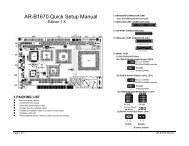
1.2 PACKING LIST<br />
In addition to this User's Manual, the <strong>AR</strong>-<strong>B1672</strong> package includes the following items:<br />
! The quick setup manual<br />
! 1 <strong>AR</strong>-<strong>B1672</strong> <strong>CPU</strong> board<br />
! 1 Hard disk drive adapter cable (40Pin)<br />
! 1 Hard disk drive adapter cable (44Pin)<br />
! 1 Floppy disk drive adapter cable<br />
! 1 Parallel port and serial port adapter cable mounted on one bracket<br />
! 1 Software utility CD<br />
! 1 PS/2 Mouse & Keyboard interface Y-cable<br />
! 1 Audio interface cable mounted on one bracket /<strong>AR</strong>-B9425A (option)<br />
! 2 USB ports on one bracket/Acrosser NO.190030136 (option)<br />
6
<strong>AR</strong>-<strong>B1672</strong> <strong>User’</strong>s <strong>Guide</strong><br />
2. INSTALLATION<br />
This chapter describes how to install the <strong>AR</strong>-<strong>B1672</strong>. At first, the layout of <strong>AR</strong>-<strong>B1672</strong> is shown, and the unpacking<br />
information that you should be careful is described. The following lists the jumpers and switches setting for the<br />
<strong>AR</strong>-<strong>B1672</strong>’s configuration.<br />
2.1 <strong>AR</strong>-<strong>B1672</strong>'S LAYOUT<br />
7
<strong>AR</strong>-<strong>B1672</strong> <strong>User’</strong>s <strong>Guide</strong><br />
2.2 POWER ON CONNECTOR FOR ATX POWER SUPPLY (ATX1)<br />
1 2 3<br />
PIN<br />
Signal<br />
1 PSON<br />
2 VCC<br />
3 5VSB<br />
* When AT power supplier is applied, jumper<br />
2&3 should be tied together. (Factory<br />
preset)<br />
* When ATX power supplier is applied,<br />
pin1&pin 3 should be connect to proper<br />
location of ATX power supplier.<br />
• ATX POWER BUTTON (BTON1)<br />
1 2<br />
Pin Signal<br />
1 -PWBN<br />
2 GND<br />
2.3 CLE<strong>AR</strong> CMOS (JP4)<br />
If want to clear the CMOS Setup (for example when you forgot the password, please clear the setup and then set<br />
the password again.), you should close the pin 2-3 about 3 seconds, then open again, set back to normal operation<br />
mode, close the pin 1-2.<br />
1<br />
3<br />
JP4<br />
1-2 ON<br />
FUNCTION<br />
Normal Operation<br />
(Factory Preset)<br />
2-3 ON Clear CMOS<br />
8
3. CONNECTION<br />
This chapter describes how to connect peripherals, switches and indicators to the <strong>AR</strong>-<strong>B1672</strong> board.<br />
3.1 AUDIO PORT CONNECTOR (AUDIO1)<br />
2<br />
1<br />
26<br />
25<br />
Pin Signal Pin Signal<br />
1 AUXAL 2 LINEL<br />
3 AUX<strong>AR</strong> 4 LINER<br />
5 +12V 6 +5V<br />
7 AUDIOL 8 MICPH<br />
<strong>AR</strong>-<strong>B1672</strong> <strong>User’</strong>s <strong>Guide</strong><br />
9 AUDIOR 10 PCSPKO<br />
11 GND 12 GND<br />
13 Not Used 14 Not Used<br />
15 GND 16 GND<br />
17 Not Used 18 Not Used<br />
19 Not Used 20 Not Used<br />
21 Not Used 22 Not Used<br />
23 Not Used 24 Not Used<br />
25 GND 26 GND<br />
Note: the connector does not contain the GAME (MIDI) port signal. When <strong>AR</strong>-B9425 audio card is used with this<br />
<strong>CPU</strong> board, the GAME port function is not supported. If users want to use the amplified trumpet that is constructed<br />
inside, please plug it into the line out. If not, please plug it into the speak-out.<br />
3.2 ULTRA ATA33/66/100 IDE DISK DRIVE CONNECTOR (IDE1, IDE2)<br />
• IDE1: Primary IDE Connector<br />
A 40-pin header type connector (IDE1) is provided to interface with up to two embedded hard disk drives (IDE AT<br />
bus). This interface, through a 40-pin cable, allows the user to connect up to two drives in a “daisy chain” fashion.<br />
To enable or disable the hard disk controller, please use the BIOS Setup program, which is explained further in<br />
chapter 5. The following table illustrates the pin assignments of the hard disk drive’s 40-pin connector.<br />
2 40<br />
1 39<br />
Pin Signal Pin Signal<br />
1 -RESET 2 GROUND<br />
3 DATA 7 4 DATA 8<br />
5 DATA 6 6 DATA 9<br />
7 DATA 5 8 DATA 10<br />
9 DATA 4 10 DATA 11<br />
11 DATA 3 12 DATA 12<br />
13 DATA 2 14 DATA 13<br />
15 DATA 1 16 DATA 14<br />
17 DATA 0 18 DATA 15<br />
19 GROUND 20 N.C<br />
21 PDDREQ 22 GROUND<br />
23 -PDIOW 24 GROUND<br />
25 -PDIOR 26 GROUND<br />
27 PIORDY 28 GROUND<br />
29 -PDDACK 30 GROUND<br />
31 IRQ14 32 N.C<br />
33 PDA1 34 PD66/100<br />
35 PDA0 36 PDA2<br />
37 -PDCS1 38 -PDCS3<br />
39 HLEDP 40 GROUND<br />
9
<strong>AR</strong>-<strong>B1672</strong> <strong>User’</strong>s <strong>Guide</strong><br />
• IDE 2: Second IDE Connector<br />
<strong>AR</strong>-<strong>B1672</strong> also provides IDE interface 44-pin connector to connect with the hard disk device.<br />
2<br />
44<br />
1<br />
43<br />
Pin Signal Pin Signal<br />
1 -RESET 2 GROUND<br />
3 DATA 7 4 DATA 8<br />
5 DATA 6 6 DATA 9<br />
7 DATA 5 8 DATA 10<br />
9 DATA 4 10 DATA 11<br />
11 DATA 3 12 DATA 12<br />
13 DATA 2 14 DATA 13<br />
15 DATA 1 16 DATA 14<br />
17 DATA 0 18 DATA 15<br />
19 GROUND 20 N.C<br />
21 SDDREQ 22 GROUND<br />
23 -SOIOW 24 GROUND<br />
25 -SOIOR 26 GROUND<br />
27 SIORDY 28 GROUND<br />
29 -SDDACK 30 GROUND<br />
31 IRQ15 32 GROUND<br />
33 SDA1 34 N.C<br />
35 SDA0 36 SD66/100<br />
37 -SDCS1 38 -SDCS3<br />
39 HLEDS 40 GROUND<br />
41 VCC 42 VCC<br />
43 GROUND 44 N.C<br />
3.3 P<strong>AR</strong>ALLEL PORT CONNECTOR (PRINT1)<br />
This port is usually connected to a printer. The <strong>AR</strong>-<strong>B1672</strong> includes an on-board parallel port, and accessed<br />
through a 26-pin flat-cable connector. Three modes –SPP, EPP and ECP – are supported.<br />
2 26<br />
1 25<br />
Pin Signal Pin Signal<br />
1 -STB 2 -AFD<br />
3 PD0 4 -ERROR<br />
5 PD1 6 -INIT<br />
7 PD2 8 -SLIN<br />
9 PD3 10 GND<br />
11 PD4 12 GND<br />
13 PD5 14 GND<br />
15 PD6 16 GND<br />
17 PD7 18 GND<br />
19 -ACK 20 GND<br />
21 BUSY 22 GND<br />
23 PE 24 GND<br />
25 SLCT 26 N.C<br />
10
<strong>AR</strong>-<strong>B1672</strong> <strong>User’</strong>s <strong>Guide</strong><br />
3.4 SERIAL PORTS (COM1, COM2)<br />
• COM1 D-SUB 9-PIN<br />
1 5<br />
6 9<br />
PIN Signal PIN Signal<br />
1 /DCD1 2 RXD1<br />
3 TXD1 4 /DTR1<br />
5 GND 6 /DSR1<br />
7 /RTS1 8 /CTS1<br />
9 /RI1 10 GND<br />
• COM2 10-pin Connector<br />
9<br />
1<br />
10 2<br />
PIN Signal PIN Signal<br />
1 /DCD2 2 /DSR2<br />
3 RXD2 4 /RTS2<br />
5 TXD2 6 /CTS2<br />
7 /DTR2 8 /RI2<br />
9 GND 10 NC<br />
3.5 COM1 RS-232/RS-485 SELECT (XP1, XP2)<br />
JUMPER<br />
FUNCTION<br />
XP1<br />
1<br />
3<br />
5<br />
XP2<br />
1<br />
2<br />
3<br />
RS-232<br />
FACTORY PRESET<br />
XP1<br />
1<br />
3<br />
5<br />
XP2<br />
1<br />
2<br />
3<br />
RS-485<br />
• RS-485 Terminator Select (J2)<br />
J2 (ON)<br />
FACTORY PRESET<br />
* When there is only one line the setting should be left off<br />
(please take off the jumper), if multiple blocks are used on a<br />
single line this should be set to “ON”(place a jumper) in order<br />
to properly terminate the connection for better transmission<br />
• RS-485 Header (J1)<br />
1<br />
2<br />
3<br />
PIN Signal<br />
1 N485+<br />
2 N485-<br />
3 GND<br />
11
<strong>AR</strong>-<strong>B1672</strong> <strong>User’</strong>s <strong>Guide</strong><br />
3.5 KEYBO<strong>AR</strong>D / MOUSE CONNECTOR (PS1, PS2)<br />
The <strong>AR</strong>-<strong>B1672</strong> provides 6-PIN JST Header and 6-PIN MINI-DIN keyboard/mouse connector.<br />
• PS1: 6-pin Mini-DIN Keyboard/Mouse Connector<br />
1 2<br />
3 4<br />
5 6<br />
Front View<br />
PIN<br />
Signal<br />
1 KBDATA<br />
2 MSDATA<br />
3 GND<br />
4 VCC<br />
5 MSCLK<br />
6 KBCLK<br />
• PS2: JST6-pin Keyboard/Mouse Connector<br />
1<br />
6<br />
PS2<br />
PIN<br />
Signal<br />
1 MSDATA<br />
2 KBDATA<br />
3 GND<br />
4 VCC<br />
5 MSCLK<br />
6 KBCLK<br />
3.6 USB PORT CONNECTOR (USB1)<br />
The <strong>AR</strong>-<strong>B1672</strong> provides Two USB port.<br />
10 9<br />
2 1<br />
PIN Signal PIN Signal<br />
1 VCC 2 VCC<br />
3 USBD0- 4 USBD1-<br />
5 USBD0+ 6 USBD1+<br />
7 GND 8 GND<br />
9 GND 10 GND<br />
3.7 IRDA INFR<strong>AR</strong>ED INTERFACE PORT (IR1)<br />
The <strong>AR</strong>-<strong>B1672</strong> built-in IrDA port which support Serial Infrared (SIR) or Amplitude Shift Keyed IR (ASKIR) interface.<br />
When use the IrDA port have to set SIR or ASKIR model in the BIOS’s Peripheral Setup’s COM 2. Then the<br />
normal RS-232 COM 2 will be disabled.<br />
1<br />
5<br />
PIN<br />
Signal<br />
1 VCC<br />
2 NC<br />
3 IRRX<br />
4 GND<br />
5 IRTX<br />
12
<strong>AR</strong>-<strong>B1672</strong> <strong>User’</strong>s <strong>Guide</strong><br />
3.8 FAN CONNECTOR (FAN1)<br />
The <strong>AR</strong>-<strong>B1672</strong> provides <strong>CPU</strong> cooling Fan connector. <strong>CPU</strong> connectors can supply 12V/500mA to the cooling fan.<br />
3 2 1<br />
PIN<br />
Signal<br />
1 GND<br />
2 +12V<br />
3 SENSE<br />
3.9 ETHERNET RJ45 CONNECTOR (LAN1)<br />
The Ethernet RJ-45 connectors are the standard network headers. The following table is the pin assignment.<br />
8<br />
1<br />
Pin Signal Pin Signal<br />
1 TX+ 5 Not Used<br />
2 TX- 6 RX-<br />
3 RX+ 7 Not Used<br />
4 Not Used 8 Not Used<br />
• ENABLED/DISABLED LAN FUNCTION (JP1)<br />
1<br />
2<br />
JP1<br />
ON<br />
OFF<br />
FUNCTION<br />
Enable On Board LAN<br />
(Factory Preset)<br />
Disabled On Board LAN<br />
3.10 VGA CRT CONNECTOR (VGA1)<br />
<strong>AR</strong>-<strong>B1672</strong> built-in 15-pin VGA connector directly to your CRT monitor.<br />
PIN Signal PIN Signal PIN Signal<br />
1 RED 6 GND 11 N.C<br />
2 GREEN 7 GND 12 SDA<br />
3 BLUE 8 GND 13 HSYNC<br />
4 N.C 9 VCC 14 VSYNC<br />
5 GND 10 GND 15 SCL<br />
13
<strong>AR</strong>-<strong>B1672</strong> <strong>User’</strong>s <strong>Guide</strong><br />
3.11 FLOPPY DRIVE CONNECTOR (FDD1)<br />
The <strong>AR</strong>-<strong>B1672</strong> provides a 34-pin header type connector for supporting up to two floppy disk drives.<br />
To enable or disable the floppy disk controller, please use the BIOS Setup program.<br />
2<br />
34<br />
1<br />
33<br />
PIN Signal PIN Signal<br />
1-33(odd) GROUND 18 DIRECTION<br />
2 DRVEN 0 20 -STEP OUTPUT PULSE<br />
4 NOT USED 22 -WRITE DATA<br />
6 DRVEN 1 24 -WRITE GATE<br />
8 -INDEX 26 -TRACK 0<br />
10 -MOTOR ENABLE 0 28 -WRITE PROTECT<br />
12 -DRIVE SELECT 1 30 -READ DATA<br />
14 -DRIVE SELECT 0 32 -SIDE 1 SELECT<br />
16 -MOTOR ENABLE 1 34 DISK CHANGE<br />
3.12 DOC SOCKET (DOC1)<br />
3.12.1 D.O.C. Memory Bank Address Select (JP2)<br />
This section provides the information about how to use the D.O.C. (Disk On Chip). It divided into two parts:<br />
hardware setting and software configuration.<br />
Step 1:<br />
Step 2:<br />
Step 3:<br />
Use JP2 to select the correct D.O.C. memory bank address.<br />
Insert programmed Disk On Chip into sockets U18 setting as DOC.<br />
Line up and insert the <strong>AR</strong>-<strong>B1672</strong> card into slot of your computer.<br />
JP2<br />
JP2<br />
ON<br />
OFF<br />
ADDRESS<br />
D000<br />
(Factory Preset)<br />
D200<br />
14
<strong>AR</strong>-<strong>B1672</strong> <strong>User’</strong>s <strong>Guide</strong><br />
3.13 GENERAL PURPOSE I/O (GPIO1)<br />
7 1<br />
8 2<br />
Pin Signal Pin Signal<br />
1 GPI0 2 GPO0<br />
3 GPI1 4 GPO1<br />
5 GPI2 6 GPO2<br />
7 GPI3 8 GPO3<br />
3.13.1 GPIO Address Select (JP3)<br />
JP3<br />
JP3<br />
ON<br />
OFF<br />
ADDRESS<br />
215H (Factory Preset)<br />
77H<br />
# Users could test GPIO function under ‘Debug’ program as follow:<br />
C:>debug<br />
# O 215 01H<br />
Generally, the GPIO2 Pin2 will be High Level, others output pin<br />
are Low Level.<br />
# I 215<br />
FC<br />
Generally, suppose that GPIO1’s Pin1 and Pin3 are High Level<br />
then will show “FC”<br />
3.14 POWER CONNECTOR (PWR1, PWR2)<br />
1 4<br />
(PWR1)<br />
PIN Signal<br />
1 +12V<br />
2 GND<br />
3 GND<br />
4 VCC (+5V)<br />
The PWR1 is a 4-pin power connector. It’s the standard connectors on all Acrosser boards.<br />
1 2<br />
PIN Signal<br />
1 -12V<br />
2 -5V<br />
(PWR2)<br />
15
<strong>AR</strong>-<strong>B1672</strong> <strong>User’</strong>s <strong>Guide</strong><br />
3.15 LCD & LVDS FUNCTION<br />
3.15.1 18-Bits LCD PANEL CONNECTOR (LCD1)<br />
2<br />
44<br />
1<br />
43<br />
PIN Signal PIN Signal PIN Signal<br />
1 GND 16 (PD18) 31 R3<br />
2 SFCLK 17 (PD19) 32 R4<br />
3 GND 18 G0 33 R5<br />
4 HSYNC 19 G1 34 GND<br />
5 VSYNC 20 GND 35 LCDVCC<br />
6 GND 21 G2 36 LCDVCC<br />
7 (PD22) 22 G3 37 +12V<br />
8 (PD23) 23 G4 38 +12V<br />
9 B0 24 G5 39 GND<br />
10 B1 25 (PD21) 40 GND<br />
11 B2 26 (PD20) 41 DE<br />
12 B3 27 GND 42 EBLT<br />
13 GND 28 R0 43 GND<br />
14 B4 29 R1 44 EVEE<br />
15 B5 30 R2<br />
3.15.2 LVDS PANEL CONNECTOR (LVDS1)<br />
2<br />
26<br />
1<br />
25<br />
PIN Signal PIN Signal<br />
1 TXOUT0- 14 GND<br />
2 GND 15 TXCLK+<br />
3 TXOUT0+ 16 VTX12<br />
4 GND 17 TXOUT3-<br />
5 TXOUT1- 18 VTX12<br />
6 LVDSVCC 19 TXOUT3+<br />
7 TXOUT1+ 20 GND<br />
8 LVDSVCC 21 VTKBP<br />
9 TXOUT2- 22 N.C<br />
10 N.C 23 LVDSVCC<br />
11 TXOUT2+ 24 N.C<br />
12 GND 25 LVDSVCC<br />
13 TXCLK- 26 N.C<br />
16
<strong>AR</strong>-<strong>B1672</strong> <strong>User’</strong>s <strong>Guide</strong><br />
3.15.3 LVDSVCC & LCDVCC VOLTAGE SELECT (LVDSV1)<br />
1 2<br />
5<br />
6<br />
LVDSV1<br />
1-3 2-4<br />
ON<br />
3-5 4-6<br />
ON<br />
VOLTAGE<br />
+3.3V<br />
(Factory Preset)<br />
+5V<br />
3.16 INTERNAL & EXTERNAL BUZZER (ESPK1)<br />
1<br />
4<br />
PIN Signal<br />
1 VCC<br />
2 SBEEP<br />
INTERNAL<br />
3<br />
BUZZER<br />
4 SBEEP<br />
PIN 1,2: Connect to External BUZZER<br />
3-4 ON (Factory Preset)<br />
Use Internal BUZZER<br />
3.17 RESET SWITCH (RST1)<br />
Shorting these two pins will reset the system.<br />
2 1<br />
PIN<br />
Signal<br />
1 RST<br />
2 GND<br />
3.18 EXTERNAL LED HEADER (LED1)<br />
7 1<br />
8 2<br />
Pin INDICATION<br />
1-2 Primary IDE Active<br />
3-4 Secondary IDE Active<br />
5-6 Watchdog Active<br />
7-8 System Power<br />
3.19 PC/104 CONNECTOR (PC-104)<br />
2<br />
64<br />
1<br />
63<br />
2<br />
40<br />
1<br />
39<br />
17
<strong>AR</strong>-<strong>B1672</strong> <strong>User’</strong>s <strong>Guide</strong><br />
4. WATCHDOG TIMER<br />
This section describes the use of Watchdog Timer, including disable, enable, and trigger. <strong>AR</strong>-<strong>B1672</strong> is equipped<br />
with a programmable time-out period watchdog timer that occupies I/O port 443H. Users can use simple program to<br />
enable the watchdog timer. Once you enable the watchdog timer, the program should trigger it every time before it<br />
times out. Watchdog Timer will generate a response (system or IRQ9) due to system fails to trigger or disable<br />
watchdog timer before preset timer, times out.<br />
Enable(D7)<br />
Time Factor<br />
(D0-D5)<br />
Write and<br />
Trigger<br />
Watchdog<br />
Register<br />
Time Base<br />
Counter and<br />
Compartor<br />
RESET<br />
Watchdog Block Diagram<br />
4.1 WATCHDOG TIMER SETTING<br />
The watchdog timer is a circuit that maybe be used from your program software to detect crash or hang up.<br />
The Watchdog timer is automatically disabled after reset. Once you enabled the watchdog timer, your program<br />
should trigger the watchdog timer every time before it times out. After you trigger the watchdog timer, the timer will<br />
be set to zero and start to count again. If your program fails to trigger the watchdog timer before times out, it will<br />
generate a reset pulse to reset the system or trigger the IRQ 9 signal in order to tell your system that the watchdog<br />
time is out.<br />
Please refer to the following table in order to properly program Watchdog function<br />
D7 D6 D5 D4 D3 D2 D1 D0<br />
1 Enable Reset<br />
Time period<br />
0 Disable IRQ 9<br />
Users could test watchdog function under ‘Debug’ program as follows:<br />
C:>debug<br />
# O 443 C8H<br />
Generally, watchdog function would reset system after 8 seconds<br />
# O 443 0<br />
Disable watchdog function<br />
C:>debug<br />
# O 443 88H<br />
Generally, watchdog function would generate IRQ 9 after 8 seconds<br />
# O 443 0H<br />
Disable watchdog function<br />
4.2 WATCHDOG TIMER TRIGGER<br />
After you enable the watchdog timer, your program must write the same factor as triggering to the watchdog timer at<br />
least once during every time-out period. You can change the time-out period by writing another timer factor to the<br />
watchdog register at any time, and you must trigger the watchdog during every new time-out period in next trigger.<br />
18
<strong>AR</strong>-<strong>B1672</strong> <strong>User’</strong>s <strong>Guide</strong><br />
5. BIOS CONSOLE<br />
This chapter describes the <strong>AR</strong>-<strong>B1672</strong> BIOS menu displays and explains how to perform common tasks needed to<br />
get up and running, and presents detailed explanations of the elements found in each of the BIOS menus. The<br />
following topics are covered:<br />
# BIOS Setup Overview<br />
# Standard CMOS Setup<br />
# Advanced CMOS Setup<br />
# Advanced Chipset Setup<br />
# Power Management<br />
# PCI/Plug and Play<br />
# Peripheral Setup<br />
# Auto-Detect Hard Disks<br />
# Password Setting<br />
# Load Default Setting<br />
# BIOS Exit<br />
5.1 BIOS SETUP OVERVIEW<br />
The BIOS is a program used to initialize and set up the I/O system of the computer, which includes the ISA bus<br />
and connected devices such as the video display, diskette drive, and the keyboard. The BIOS provides a<br />
menu-based interface to the console subsystem. The console subsystem contains special software, called<br />
firmware that interacts directly with the hardware components and facilitates interaction between the system<br />
hardware and the operating system.<br />
The BIOS default values ensure that the system will function at its normal capability. In the worst situation the user<br />
may have corrupted the original settings set by the manufacturer.<br />
After the computer is turned on, the BIOS will perform diagnostics on the system and display the size of the<br />
memory that is being tested. Press the [Del] key to enter the BIOS Setup program, and then the main menu will<br />
show on the screen.<br />
The BIOS Setup main menu includes some options. Use the [Up/Down] arrow key to highlight the option that you<br />
wish to modify, and then press the [Enter] key to select the option and configure the functions.<br />
Setup Main Menu<br />
CAUTION:<br />
1. <strong>AR</strong>-<strong>B1672</strong> BIOS the factory-default setting is used to the Acrosser<br />
recommends using the BIOS default setting, unless you are very familiar with the setting function, or you can<br />
contact the technical support engineer.<br />
2. If the BIOS settings are lost, the CMOS will detect the to boot the<br />
operation system, this option will reduce the performance of the system. Acrosser recommends choosing the<br />
in the main menu. This option gives best-case values that should<br />
optimize system performance.<br />
3. The BIOS settings are described in detail in this section.<br />
19
<strong>AR</strong>-<strong>B1672</strong> <strong>User’</strong>s <strong>Guide</strong><br />
5.2 STAND<strong>AR</strong>D CMOS SETUP<br />
The option allows you to record some basic system hardware configuration and set the<br />
system clock and error handling. If the <strong>CPU</strong> board is already installed in a working system, you will not need to<br />
select this option anymore.<br />
Standard CMOS Setup<br />
Date & Time Setup<br />
Highlight the field and then press the [Page Up] /[Page Down] or [+]/[-] keys to set the current date. Follow<br />
the month, day and year format.<br />
Highlight the field and then press the [Page Up] /[Page Down] or [+]/[-] keys to set the current date. Follow<br />
the hour, minute and second format.<br />
The user can bypass the date and time prompts by creating an AUTOEXEC.BAT file. For information on how to<br />
create this file, please refer to the MS-DOS manual.<br />
Hard Disk Setup<br />
The BIOS supports various types for user settings, The BIOS supports , , <br />
and so the user can install up to two hard disks. For the master and slave jumpers, please refer to<br />
the hard disk’s installation descriptions and the hard disk jumper settings in section three of this manual.<br />
You can select under the and fields. This will enable auto detection of your IDE drives<br />
during boot-up. This will allow you to change your hard drives (with the power off) and then power on without having<br />
to reconfigure your hard drive type. If you use older hard disk drives, which do not support this feature, then you<br />
must configure the hard disk drive in the standard method as described above by the option.<br />
Floppy Setup<br />
The option records the types of floppy disk drives installed in the system.<br />
To enter the configuration value for a particular drive, highlight its corresponding field and then select the drive type<br />
using the left-or right-arrow key.<br />
Boot Sector Virus Protection<br />
This option protects the boot sector and partition table of your hard disk against accidental modifications. Any<br />
attempt to write to them will cause the system to halt and display a warning message. If this occurs, you can either<br />
allow the operation to continue or use a bootable virus-free floppy disk to reboot and investigate your system. The<br />
default setting is . This setting is recommended because it conflicts with new operating systems.<br />
Installation of new operating systems requires that you disable this to prevent write errors.<br />
20
<strong>AR</strong>-<strong>B1672</strong> <strong>User’</strong>s <strong>Guide</strong><br />
5.3 ADVANCED CMOS SETUP<br />
The option consists of configuration entries that allow you to improve your system<br />
performance, or let you set up some system features according to your preference. Some entries here are<br />
required by the <strong>CPU</strong> board’s design to remain in their default settings.<br />
Advanced CMOS Setup<br />
Quick Boot<br />
This category speeds up Power On Self Test (POST) after you power on the computer. If it is set to Enabled,<br />
BIOS will shorten or skip some check items during POST.<br />
1st Boot Device<br />
2nd Boot Device<br />
3rd Boot Device<br />
4th Boot Device<br />
These options determine where the system looks first for an operating system.<br />
S.M.A.R.T for Hard Disks<br />
S.M.A.R.T is abbreviation of Self-Monitoring Analysis and Reporting Technology. It is reliable and precautious<br />
technology. When Hard Disk disorder, it prevents Hard Disk from the loss of data.<br />
Boot Up Num-Lock<br />
This item is used to activate the Num-Lock function upon system boot. If the setting is on, after a boot, the<br />
Num-Lock light is lit, and user can use the number key.<br />
Floppy Drive Swap<br />
The option reverses the drive letter assignments of your floppy disk drives in the Swap A, B setting, otherwise leave<br />
on the setting of Disabled (No Swap). This works separately from the BIOS Features floppy disk swap feature. It<br />
is functionally the same as physically interchanging the connectors of the floppy disk drives. When , the<br />
BIOS swapped floppy drive assignments so that Drive A becomes Drive B, and Drive B becomes Drive A under<br />
DOS.<br />
Floppy Drive Seek<br />
If the item is setting Enabled, the BIOS will seek the floppy drive one time upon boot up.<br />
21
<strong>AR</strong>-<strong>B1672</strong> <strong>User’</strong>s <strong>Guide</strong><br />
PS/2 Mouse Support<br />
The setting of Enabled allows the system to detect a PS/2 mouse on boot up. If detected, IRQ12 will be used for<br />
the PS/2 mouse. IRQ 12 will be reserved for expansion cards if a PS/2 mouse is not detected. Disabled will<br />
reserve IRQ12 for expansion cards and therefore the PS/2 mouse will not function.<br />
Primary Display<br />
The option is used to set the type of video display card installed in the system.<br />
Password Check<br />
This option enables password checking every time the computer is powered on or every time the BIOS Setup is<br />
executed. If Always is chosen, a user password prompt appears every time the computer is turned on. If Setup is<br />
chosen, the password prompt appears if the BIOS executed.<br />
Boot to OS/2<br />
When using the OS/2 operating system, you need to Yes this option otherwise leave this on the setup default of No.<br />
System BIOS Cacheable<br />
Enabled this option to enhance system performance by shadowing and caching system BIOS shadow functions will<br />
be ignored.<br />
Shadow Memory<br />
Each of segments provides three options Disabled, Enabled, and Cached for faster adapter’s ROM executions.<br />
However this shadow function is Chipset oriented and dependent on system hardware feature. In general, C000<br />
64K will be allocated for VGA BIOS and set to Cached to get higher display performance by shadowing and caching<br />
feature. If user chooses Enabled setting, only BIOS shadow function is active.<br />
22
<strong>AR</strong>-<strong>B1672</strong> <strong>User’</strong>s <strong>Guide</strong><br />
5.4 ADVANCED CHIPSET SETUP<br />
This option controls the configuration of the board’s chipset. Control keys for this screen are the same as for the<br />
previous screen.<br />
Advanced Chipset Setup<br />
Configure SDRAM Timing by SPD<br />
SPD is the abbreviation Serial Presence Detect. SPD takes accord the chip types, capacity, timing, voltage data.<br />
The system can auto adjust memory according to the data to reach the best situation.<br />
The Choice: Enabled, Disabled<br />
DRAM Frequency<br />
PC-100 means the memory bus is running at 100MHz. PC-133 means the memory bus is running at 133MHz.<br />
The Choice: 66Mhz, 100Mhz, 133Mhz<br />
SDRAM CAS Latency Time<br />
When synchronous DRAM is installed, the number of clock cycles of CAS latency depends on the DRAM timing.<br />
The Choice: 2, 3<br />
Memory Hole<br />
You can reserve this area of system memory for ISA adapter ROM. When this area is reserved, it cannot be cached.<br />
The user information of peripherals that need to use this area of system memory usually discusses their memory<br />
requirements.<br />
AGP Aperture Size<br />
The item is to set up AGP display to use how much memory to save Texture Data.<br />
USB Controller<br />
This option can enable USB Port 0&1or Disabled USB function.<br />
USB Device Legacy Support<br />
These options are used to enable the USB function and it’s only useful in the DOS mode. The USB function sets<br />
Enabled will occupy IRQ10.<br />
23
<strong>AR</strong>-<strong>B1672</strong> <strong>User’</strong>s <strong>Guide</strong><br />
5.5 POWER MANAGEMENT<br />
This section is used to configure power management features. This option allows<br />
you to reduce power consumption. This feature turns off the video display and shuts down the hard disk after a<br />
period of inactivity.<br />
Power Management<br />
ACPI Aware O/S<br />
The option YES is for ATX power, the option NO is for AT Power.<br />
System Thermal<br />
If the choice is chose, the system will alarm when the system temperature is beyond the critical<br />
temperature.<br />
Thermal Active Temperature<br />
Thermal Slow Clock Ratio<br />
This item is to set up the Operating Frequency of system clock in power saving mode, to set a suitable clock<br />
frequency ratio, which between standard <strong>CPU</strong> clock and <strong>CPU</strong> clock in power saving mode when the temperature is<br />
beyond the critical temperature.<br />
24
<strong>AR</strong>-<strong>B1672</strong> <strong>User’</strong>s <strong>Guide</strong><br />
5.6 PCI/PLUG AND PLAY<br />
This section is used to configure PCI / Plug and Play features. The option configures the PCI<br />
bus slots.<br />
PCI / Plug And Play<br />
Plug and Play Aware O/S<br />
Set this option to Yes if the operating system installed in the computer is Plug and Play-aware. The BIOS only<br />
detects and enables PnP ISA adapter cards that are required for system boot. The Windows 95 operating system<br />
detects and enables all other PnP-aware adapter cards. Windows 95 is PnP-aware. Set this option if the<br />
operating system (such as DOS, OS/2, Windows 3.x) does not use PnP. You must set this option correctly or<br />
PnP-aware adapter cards installed in your computer will not be configured properly.<br />
Clear NVRAM<br />
This sets the operating mode of the boot block area of the BIOS FLASH ROM to allow programming in the Yes<br />
setting.<br />
PCI Latency Timer (PCI Clocks)<br />
This option sets latency of all PCI devices on the PCI bus. The settings are in units equal to PCI clocks.<br />
Primary Graphic Adapter<br />
This option is set to use PCI bus or AGP. The AGP mode will get system a faster processing speed.<br />
DMA & IRQ<br />
These options specify the bus that the named IRQs/DMAs lines are used on. These options allow you to specify<br />
IRQs/DMAs for use by legacy ISA adapter cards. These options determine if the BIOS should remove an IRQ/DMA<br />
from the pool of availability of IRQs/DMAs passed to the BIOS configurable devices. If more IRQs/DMAs must be<br />
removed from the pool, the end user can use these PCI/PnP Setup options to remove the IRQ/DMA by assigning<br />
the option to the ISA/EISA setting. The onboard I/O is configurable with BIOS.<br />
25
<strong>AR</strong>-<strong>B1672</strong> <strong>User’</strong>s <strong>Guide</strong><br />
5.7 PERIPHERAL SETUP<br />
This section is used to configure peripheral features.<br />
Peripheral Setup<br />
OnBoard FDC<br />
This option enables the floppy drive controller on the <strong>AR</strong>-<strong>B1672</strong>.<br />
OnBoard Serial Port<br />
This option enables the serial port on the <strong>AR</strong>-<strong>B1672</strong>.<br />
IR Port support<br />
This item is to activate the function of Infrared.<br />
OnBoard Parallel Port<br />
This option enables the parallel port on the <strong>AR</strong>-<strong>B1672</strong>.<br />
Parallel Port Mode<br />
This option specifies the parallel port mode. ECP and EPP are both bi-directional data transfer schemes that<br />
adhere to the IEEE 284 specifications.<br />
Parallel Port DMA Channel<br />
This option is only available if the setting for the parallel Port Mode option is ECP.<br />
OnBoard IDE<br />
This option is to set up the operating mode of IDE controller. If the main board offers the enhanced I/O port, the<br />
choice should be .<br />
OnBoard AC’97 Audio<br />
This item allows you to decide to Enabled, Disabled the AC’97 Audio.<br />
26
<strong>AR</strong>-<strong>B1672</strong> <strong>User’</strong>s <strong>Guide</strong><br />
5.8 AUTO-DETECT H<strong>AR</strong>D DISKS<br />
This option detects the parameters of an IDE hard disk drive, and automatically enters them into the Standard<br />
CMOS Setup screen.<br />
5.9 PASSWORD SETTING<br />
This BIOS Setup has an optional password feature. The system can be configured so that all users must enter a<br />
password every time the system boots or when BIOS Setup is executed. User can set either a Supervisor<br />
password or a User password.<br />
Select the appropriate password icon (Supervisor or User) from the Security section of the BIOS Setup main menu.<br />
Enter the password and press [Enter]. The screen does not display the characters entered. After the new<br />
password is entered, retype the new password as prompted and press [Enter].<br />
If the password confirmation is incorrect, an error message appears. If the new password is entered without error,<br />
press [Esc] to return to the BIOS Main Menu. The password is stored in CMOS RAM after BIOS completes.<br />
The next time the system boots, you are prompted for the password function is present and is enabled.<br />
Enter new supervisor password:<br />
5.10 LOAD DEFAULT SETTING<br />
This section permits users to select a group of settings for all BIOS Setup options. You not only can use these<br />
items to quickly set system configuration parameters, but also can choose a group of settings that have a better<br />
chance of working when the system is having configuration related problems.<br />
5.10.1 Auto Configuration with Optimal Setting<br />
The user can load the optimal default settings for the BIOS. The Optimal default settings are best-case values that<br />
should optimize system performance. If CMOS RAM is corrupted, the optimal settings are loaded automatically.<br />
Load high performance setting (Y/N) ? Y<br />
5.10.2 Auto Configuration with Fail Safe Setting<br />
The user can load the Fail-Safe BIOS Setup option settings by selecting the Fail-Safe item from the Default section<br />
of the BIOS Setup main menu.<br />
The Fail-Safe settings provide far from optimal system performance, but are the most stable settings. Use this<br />
option as a diagnostic aid if the system is behaving erratically.<br />
Load failsafe settings (Y/N) ? Y<br />
5.11 BIOS EXIT<br />
This section is used to exit the BIOS main menu. After making your changes, you can either save them or exit the<br />
BIOS menu and without saving the new values.<br />
27
<strong>AR</strong>-<strong>B1672</strong> <strong>User’</strong>s <strong>Guide</strong><br />
5.12 BIOS UPDATE<br />
The BIOS program instructions are contained within computer chips called FLASH ROMs that are located on your<br />
system board. The chips can be electronically reprogrammed, allowing you to upgrade your BIOS firmware<br />
without removing and installing chips.<br />
The <strong>AR</strong>-<strong>B1672</strong> provides the FLASH BIOS update function for you to easily to update to a newer BIOS version.<br />
Please follow these operating steps to update to new BIOS:<br />
Step 1:<br />
Step 2:<br />
Step 3:<br />
Turn on your system and don’t detect the CONFIG.SYS and AUTOEXEC.BAT files.<br />
Insert the FLASH BIOS diskette into the floppy disk drive.<br />
In the MS-DOS mode, you can type the FLASH826 program.<br />
A:\>FLASH826<br />
Step 4:<br />
Press [ALT+F], The box will show the following message, this message will be highlighted.<br />
BIOS Filename Loading … . After typing in the File name you must press or press<br />
to exit.<br />
Step 5: And then please enter the file name to the box. And the box will<br />
show the following notice.<br />
Are you sure to write the BIOS into flash ROM?<br />
Step 6:<br />
Press the key to update the new BIOS.<br />
Then the box will show the .<br />
Step 7: When the BIOS update is successful, the message will show .<br />
28
<strong>AR</strong>-<strong>B1672</strong> <strong>User’</strong>s <strong>Guide</strong><br />
APPENDIX A. ADDRESS MAPPING<br />
IO Address Map<br />
I/O MAP<br />
ASSIGNMENT<br />
000-01F DMA controller (Master)<br />
020-021 Interrupt controller (Master)<br />
022-023 Chipset controller registers I/O ports.<br />
040-05F Timer control registers.<br />
060-06F Keyboard interface controller<br />
070-07F RTC ports & CMOS I/O ports<br />
080-09F DMA register<br />
0A0-0BF<br />
Interrupt controller (Slave)<br />
0C0-0DF<br />
DMA controller (Slave)<br />
0F0-0FF<br />
Math coprocessor<br />
1F0-1F8<br />
Hard Disk controller<br />
250-258 Super I/O<br />
2B0-2DF<br />
Graphics adapter controller<br />
2F8-2FF<br />
Serial port-2<br />
360-36F Net work ports<br />
378-37F Parallel port<br />
3B0-3BF<br />
Monochrome & Printer adapter<br />
3C0-3CF<br />
EGA adapter<br />
3D0-3DF<br />
CGA adapter<br />
3F0-3F7<br />
Floppy disk controller<br />
3F8-3FF<br />
Serial port-1<br />
Memory Map:<br />
MEMORY MAP<br />
0000000-009FFFF<br />
00A0000-00BFFFF<br />
00C0000-00DFFFF<br />
00E0000-00EFFFF<br />
00F0000-00FFFFF<br />
0100000-FFFFFFF<br />
ASSIGNMENT<br />
System memory used by DOS and application<br />
Display buffer memory for VGA/ EGA / CGA /<br />
MONOCHROME adapter<br />
Reserved for I/O device BIOS ROM or RAM buffer.<br />
Reserved for PCI device ROM<br />
System BIOS ROM<br />
System extension memory<br />
29
<strong>AR</strong>-<strong>B1672</strong> <strong>User’</strong>s <strong>Guide</strong><br />
APPENDIX B. INTERRUPT REQUEST (IRQ)<br />
SETTING H<strong>AR</strong>DW<strong>AR</strong>E USING THE SETTING<br />
00 System timer<br />
01 Standard 101/102-Key or Microsoft Natural Keyboard<br />
02 Programmable interrupt controller<br />
03 Serial Port (COM2)<br />
04 Serial Port (COM1)<br />
05 IRQ Holder for PCI Steering<br />
06 Floppy Disk Controller<br />
07 Parallel Port (LPT1)<br />
08 RTC clock<br />
09 ACPI<br />
12 PS/2 Compatible Mouse Port<br />
13 Numeric data processor<br />
14 Primary IDE controller<br />
15 Secondary IDE controller<br />
Note:<br />
If the content in Setting is inconsistent with CD-ROM. Please refer to the Setting as priority.<br />
30