Half Size All-In-One 386SX CPU CARD User’ s Guide
AR-B1375/AR-B1376 Half Size All-In-One 386SX CPU ... - Acrosser
AR-B1375/AR-B1376 Half Size All-In-One 386SX CPU ... - Acrosser
- No tags were found...

You also want an ePaper? Increase the reach of your titles
YUMPU automatically turns print PDFs into web optimized ePapers that Google loves.
AR-B1375/AR-B1376<br />
<strong>Half</strong> <strong>Size</strong> <strong>All</strong>-<strong>In</strong>-<strong>One</strong><br />
<strong>386SX</strong> <strong>CPU</strong> <strong>CARD</strong><br />
<strong>User’</strong> s <strong>Guide</strong><br />
Edition: 1.52<br />
Book Number: AR-B1375/AR-B1376-05.0708
AR-B1375/AR-B1376 Users <strong>Guide</strong><br />
Table of Contents<br />
0. PREFACE ...........................................................................................................................................................0-3<br />
0.1 COPYRIGHT NOTICE AND DISCLAIMER............................................................................................................................ 0-3<br />
0.2 WELCOME TO THE AR-B1375/AR-B1376 <strong>CPU</strong> BOARD ..................................................................................................... 0-3<br />
0.3 BEFORE YOU USE THIS GUIDE.......................................................................................................................................... 0-3<br />
0.4 RETURNING YOUR BOARD FOR SERVICE ....................................................................................................................... 0-3<br />
0.5 TECHNICAL SUPPORT AND USER COMMENTS ............................................................................................................... 0-3<br />
0.6 ORGANIZATION .................................................................................................................................................................... 0-4<br />
0.7 STATIC ELECTRICITY PRECAUTIONS ............................................................................................................................... 0-4<br />
1. OVERVIEW.........................................................................................................................................................1-1<br />
1.1 INTRODUCTION.................................................................................................................................................................... 1-1<br />
1.2 PACKING LIST....................................................................................................................................................................... 1-1<br />
1.3 FEATURES ............................................................................................................................................................................ 1-2<br />
2. SYSTEM CONTROLLER....................................................................................................................................2-1<br />
2.1 MICROPROCESSOR ............................................................................................................................................................ 2-1<br />
2.2 DMA CONTROLLER.............................................................................................................................................................. 2-1<br />
2.3 KEYBOARD CONTROLLER.................................................................................................................................................. 2-2<br />
2.4 INTERRUPT CONTROLLER ................................................................................................................................................. 2-2<br />
2.4.1 I/O Port Address Map..................................................................................................................................................... 2-3<br />
2.4.2 I/O Channel Pin Assignment (Bus 1) ............................................................................................................................. 2-3<br />
2.5 REAL-TIME CLOCK AND NON-VOLATILE RAM.................................................................................................................. 2-5<br />
2.6 TIMER .................................................................................................................................................................................... 2-5<br />
2.7 SERIAL PORT........................................................................................................................................................................ 2-6<br />
2.8 PARALLEL PORT .................................................................................................................................................................. 2-8<br />
3. SETTING UP THE SYSTEM...............................................................................................................................3-1<br />
3.1 OVERVIEW ............................................................................................................................................................................ 3-1<br />
3.2 SYSTEM SETTING ................................................................................................................................................................ 3-2<br />
3.2.1 Keyboard Connector ...................................................................................................................................................... 3-2<br />
3.2.2 PC/104 Connector.......................................................................................................................................................... 3-3<br />
3.2.3 Hard Disk (IDE) Connector (CN4).................................................................................................................................. 3-5<br />
3.2.4 FDD Port Connector (CN5) ............................................................................................................................................ 3-6<br />
3.2.5 Parallel Port Connector (CN6) ....................................................................................................................................... 3-6<br />
3.2.6 Serial Port....................................................................................................................................................................... 3-7<br />
3.2.7 Reset Header (J1).......................................................................................................................................................... 3-8<br />
3.2.8 LED Header.................................................................................................................................................................... 3-8<br />
3.2.9 Power Connector (J3) .................................................................................................................................................... 3-9<br />
3.2.10 External Speaker Header (J5)........................................................................................................................................ 3-9<br />
3.2.11 External Battery.............................................................................................................................................................. 3-9<br />
3.2.12 <strong>CPU</strong> Base Clock Select (JP1)...................................................................................................................................... 3-10<br />
3.2.13 DRAM Configuration .................................................................................................................................................... 3-10<br />
4. CRT/LCD FLAT PANEL DISPLAY.....................................................................................................................4-1<br />
4.1 CONNECTING THE CRT MONITOR..................................................................................................................................... 4-1<br />
4.1.1 VGA Setting (JP5).......................................................................................................................................................... 4-1<br />
4.1.2 CRT Connector (DB1).................................................................................................................................................... 4-2<br />
4.2 LCD FLAT PANEL DISPLAY ................................................................................................................................................. 4-2<br />
4.2.1 <strong>In</strong>verter Board Description ............................................................................................................................................. 4-3<br />
4.2.2 LCD Connector............................................................................................................................................................... 4-3<br />
4.3 SUPPORTED LCD PANEL .................................................................................................................................................... 4-4<br />
5. INSTALLATION..................................................................................................................................................5-1<br />
5.1 OVERVIEW ............................................................................................................................................................................ 5-1<br />
5.2 UTILITY DISKETTE ............................................................................................................................................................... 5-1<br />
5.2.1 VGA Driver ..................................................................................................................................................................... 5-2<br />
5.2.2 SSD Utility ...................................................................................................................................................................... 5-3<br />
5.3 WRITE PROTECT FUNCTION .............................................................................................................................................. 5-5<br />
5.3.1 Hardware Write Protect.................................................................................................................................................. 5-6<br />
5.3.2 Software Write Protect ................................................................................................................................................... 5-6<br />
5.3.3 Enable the Software Write Protect ................................................................................................................................. 5-6<br />
5.3.4 Disable the Software Write Protect ................................................................................................................................ 5-6<br />
5.4 WATCHDOG TIMER.............................................................................................................................................................. 5-7<br />
5.4.1 Watchdog Timer Setting................................................................................................................................................. 5-7<br />
5.4.2 Watchdog Timer Enabled............................................................................................................................................... 5-8<br />
5.4.3 Watchdog Timer Trigger................................................................................................................................................. 5-8<br />
5.4.4 Watchdog Timer Disabled.............................................................................................................................................. 5-8<br />
6. SOLID STATE DISK ...........................................................................................................................................6-1<br />
6.1 OVERVIEW ............................................................................................................................................................................ 6-1<br />
0-1
AR-B1375/AR-B1376 Users <strong>Guide</strong><br />
6.2 SWITCH SETTING................................................................................................................................................................. 6-1<br />
6.2.1 Overview ........................................................................................................................................................................ 6-2<br />
6.2.2 I/O Port Address Select (SW1-1) ................................................................................................................................... 6-2<br />
6.2.3 SSD Firmware Address Select (SW1-2) ........................................................................................................................ 6-2<br />
6.2.4 SSD Drive Number (SW1-3 & SW1-4)........................................................................................................................... 6-3<br />
6.2.5 ROM Type Select (SW1-5 & SW1-6) ............................................................................................................................. 6-4<br />
6.3 JUMPER SETTING ................................................................................................................................................................ 6-5<br />
6.4 ROM DISK INSTALLATION ................................................................................................................................................... 6-6<br />
6.4.1 UV EPROM (27Cxxx)..................................................................................................................................................... 6-6<br />
6.4.2 Large Page 5V FLASH Disk........................................................................................................................................... 6-7<br />
6.4.3 Small Page 5V FLASH ROM Disk ................................................................................................................................. 6-9<br />
6.4.4 RAM Disk ..................................................................................................................................................................... 6-10<br />
6.4.5 Combination of ROM and RAM Disk............................................................................................................................ 6-11<br />
7. BIOS CONSOLE.................................................................................................................................................7-1<br />
7.1 BIOS SETUP OVERVIEW ..................................................................................................................................................... 7-1<br />
7.2 STANDARD CMOS SETUP......................................................................................................................................................... 7-2<br />
7.3 ADVANCED CMOS SETUP......................................................................................................................................................... 7-3<br />
7.4 ADVANCED CHIPSET SETUP.................................................................................................................................................... 7-6<br />
7.5 POWER MANAGEMENT SETUP ................................................................................................................................................ 7-8<br />
7.6 PCI / PLUG AND PLAY SETUP................................................................................................................................................... 7-9<br />
7.7 PERIPHERAL SETUP................................................................................................................................................................ 7-10<br />
7.8 AUTO-DETECT HARD DISKS................................................................................................................................................... 7-11<br />
7.9 PASSWORD SETTING.............................................................................................................................................................. 7-11<br />
7.10 LOAD DEFAULT SETTING...................................................................................................................................................... 7-12<br />
7.10.1 Auto Configuration with Optimal Setting............................................................................................................................ 7-12<br />
7.10.2 Auto Configuration with Fail Safe Setting.......................................................................................................................... 7-12<br />
7.11 BIOS EXIT ................................................................................................................................................................................ 7-12<br />
7.11.1 Save Settings and Exit ...................................................................................................................................................... 7-12<br />
7.11.2 Exit Without Saving ........................................................................................................................................................... 7-12<br />
7.12 BIOS UPDATE ......................................................................................................................................................................... 7-12<br />
8. SPECIFICATIONS & SSD TYPES SUPPORTED ..............................................................................................8-1<br />
8.1 SPECIFICATIONS ................................................................................................................................................................. 8-1<br />
8.2 SSD TYPES SUPPORTED.................................................................................................................................................... 8-1<br />
9. USING MEMORY BANKS ..................................................................................................................................9-1<br />
10. PLACEMENT & DIMENSIONS.........................................................................................................................10-1<br />
10.1 PLACEMENT ................................................................................................................................................................... 10-1<br />
10.2 DIMENSIONS................................................................................................................................................................... 10-2<br />
11. PROGRAMMING RS-485 & INDEX..................................................................................................................11-1<br />
11.1 PROGRAMMING RS-485 ................................................................................................................................................ 11-1<br />
11.2 INDEX .............................................................................................................................................................................. 11-3<br />
0-2
AR-B1375/AR-B1376 Users <strong>Guide</strong><br />
0.PREFACE<br />
0.1 COPYRIGHT NOTICE AND DISCLAIMER<br />
September 1997<br />
This document is copyrighted, 1997, by Acrosser Technology Co., Ltd. <strong>All</strong> rights are reserved. No part of this<br />
manual may be reproduced, copied, transcribed, stored in a retrieval system, or translated into any language in<br />
any form or by any means, such as electronic, mechanical, magnetic, optical, chemical, manual or other means<br />
without prior written permission of original manufacturer.<br />
Acrosser Technology assumes no responsibility or warranty with respect to the contents in this manual and<br />
specifically disclaims any implied warranties of merchantability or fitness for any particular purpose. Furthermore,<br />
Acrosser Technology reserves the right to make improvements to the products described in this manual at any<br />
times without notice. Such revisions will be posted on the <strong>In</strong>ternet (WWW.ACROSSER.COM) as soon as possible.<br />
Possession, use, or copying of the software described in this publication is authorized only pursuant to a valid<br />
written license from Acrosser or an authorized sub licensor.<br />
ACKNOWLEDGEMENTS<br />
(C) Copyright Acrosser Technology Co., Ltd., 1997. <strong>All</strong> rights Reserved.<br />
Acrosser, ALI, AMI, PC/AT, WIN31, WIN 95, Windows NT, NEC, HITACHI, ORION, SHARP, FUJITSU, SONY, AKM,<br />
INTEL, MITSUBISHI, NS, SGS-THOMSON, TI, TOSHIBA, AMD…are registered trademarks.<br />
<strong>All</strong> other trademarks and registered trademarks are the property of their respective holders.<br />
This document was produced with Adobe Acrobat 3.01.<br />
0.2 WELCOME TO THE AR-B1375/AR-B1376 <strong>CPU</strong> BOARD<br />
This guide introduces the Acrosser AR-B1375/AR-B1376 <strong>CPU</strong> board.<br />
The information provided in this manual describes this card’s functions, and features. It also helps you start, set<br />
up and operate your AR-B1375/AR-B1376. General system information can also be found in this publication.<br />
0.3 BEFORE YOU USE THIS GUIDE<br />
Please refer to the Chapter 3, “Setting Up the System” in this guide, if you have not already installed AR-<br />
B1375/AR-B1376,. Check the packing list before you install and make sure the accessories in the package.<br />
The AR-B1375 & AR-B1376 diskette provides the newest information regarding the <strong>CPU</strong> card. Please refer to<br />
the README.DOC file of the enclosed utility diskette. It contains the modification and hardware & software<br />
information, and it has updated to product functions that may not be mentioned here..<br />
0.4 RETURNING YOUR BOARD FOR SERVICE<br />
If your board requires any services, contact the distributor or sales representative from whom you purchased the<br />
product for service information. If you need to ship your board to us for service, be sure it is packed in a protective<br />
carton. We recommend that you keep the original shipping container for this purpose.<br />
You can help assure efficient servicing for your product by following these guidelines:<br />
1. <strong>In</strong>clude your name, address, telephone and facsimile number where you may be reached during the day.<br />
2. A description of the system configuration and/or software at the time is malfunction.<br />
3. A brief description of problem occurred.<br />
0.5 TECHNICAL SUPPORT AND USER COMMENTS<br />
<strong>User’</strong>s comments are always welcome as they assist us in improving the quality of our products and the<br />
readability of our publications. They create a very important part of the input used for product enhancement and<br />
revision.<br />
We may use and distribute any of the information you provide in any way appropriate without incurring any<br />
obligation. You may, of course, continue to use the information you provide.<br />
If you have any suggestions for improving particular sections or if you find any errors, please send your<br />
comments to Acrosser Technology Co., Ltd. or your local sales representative and indicate the manual title and<br />
book number.<br />
<strong>In</strong>ternet electronic mail to: webmaster@acrosser.com<br />
0-3
AR-B1375/AR-B1376 Users <strong>Guide</strong><br />
0.6 ORGANIZATION<br />
This information for users covers the following topics (see the Table of Contents for a detailed listing):<br />
• Chapter 1, “Overview,” provides an overview of the system features and packing list.<br />
• Chapter 2, “System Controller,” describes the major structure.<br />
• Chapter 3, “Setting Up the System,” describes how to adjust the jumper, and the connectors setting.<br />
• Chapter 4, “CRT/LCD Flat Panel Display”, describes the configuration and installation procedure using<br />
LCD and CRT display.<br />
• Chapter 5, “<strong>In</strong>stallation,” describes the utility diskette using, solid-state disk’s writing protect function, and<br />
the watchdog timer.<br />
• Chapter 6, “Solid State Disk,” describes the various type SSD’s installation steps.<br />
• Chapter 7, “BIOS Console,” providing the BIOS options setting.<br />
• Chapter 8, Specifications & SSD Types Supported<br />
• Chapter 9, Using Memory Banks<br />
• Chapter 10, Placement & Dimensions<br />
• Chapter 11, Programming RS-485 & <strong>In</strong>dex<br />
0.7 STATIC ELECTRICITY PRECAUTIONS<br />
Before removing the board from its anti-static bag, read this section about static electricity precautions.<br />
Static electricity is a constant danger to computer systems. The charge that can build up in your body may be<br />
more than sufficient to damage integrated circuits on any PC board. It is, therefore, important to observe basic<br />
precautions whenever you use or handle computer components. Although areas with humid climates are much<br />
less prone to static build-up, it is always best to safeguard against accidents may result in expensive repairs. The<br />
following measures should generally be sufficient to protect your equipment from static discharge:<br />
• Touch a grounded metal object to discharge the static electricity in your body (or ideally, wear a grounded<br />
wrist strap).<br />
• When unpacking and handling the board or other system component, place all materials on an antic static<br />
surface.<br />
• Be careful not to touch the components on the board, especially the “golden finger” connectors on the bottom<br />
of every board.<br />
0-4
AR-B1375/AR-B1376 Users <strong>Guide</strong><br />
1. OVERVIEW<br />
This chapter provides an overview of your system features and capabilities. The following topics are covered:<br />
• <strong>In</strong>troduction<br />
• Packing List<br />
• Features<br />
1.1 INTRODUCTION<br />
The AR-B1375 and AR-B1376 are new generation half size, 386 ISA card. This card offers much greater performance<br />
than the older cards such as support for 32MB’s of DRAM using two 72-pin SIMMs, one RS-232C/485 and one RS-232C<br />
port and 3/1.5MB solid state disk capacity for ROM, FLASH and SRAM.<br />
The unit also comes with a programmable watchdog timer and other typical interfaces. These 386 <strong>CPU</strong> cards are excellent<br />
for embedded systems, MMI’s, workstations, medical applications or POS/POI systems. As well, an RS-232C/485 port<br />
provided remote control. RS-485 has not been offered until recently on 386 cards.<br />
Especially the AR-B1376 with on board VGA, offers the most exciting possibilities yet to the industry. The on board<br />
VGA/LCD controller brings about a whole new dimension of industrial computing. No longer do you have to worry about<br />
adding an extra card to your system. Negating the need of a separate VGA card saves space. The VGA/LCD unit comes<br />
with 1MB of V-RAM on board and uses the C&T 65545 Chipset, to support a wide range of LCD Panels.<br />
1.2 PACKING LIST<br />
The accessories are included with the system. Before you begin installing your AR-B1375 or AR-B1376 board,<br />
take a moment to make sure that the following items have been included inside the AR-B1375 or AR-B1376<br />
package.<br />
• The quick setup manual<br />
• 1 AR-B1375 or AR-B1376 all-in-one single <strong>CPU</strong> board<br />
• 1 Hard disk drive interface cable<br />
• 1 Floppy disk drive interface cable<br />
• 1 Parallel port interface cable<br />
• 1 RS-232C interface cable<br />
• 2 Software utility CD (AR-B1375 has not the VGA function, and only encloses one SSD utility<br />
diskette).<br />
1-1
AR-B1375/AR-B1376 Users <strong>Guide</strong><br />
1.3 FEATURES<br />
The system provides a number of special features that enhance its reliability, ensure its availability, and improve its<br />
expansion capabilities, as well as its hardware structure.<br />
• 80<strong>386SX</strong>-33/40 MHz <strong>CPU</strong><br />
• ISA and PC/104 extension bus<br />
• Up to 32MB DRAM system<br />
• On-board CRT and LCD panel display (AR-B1375 doesn’t provide this function)<br />
• Supports IDE hard disk drives<br />
• Supports floppy disk drives<br />
• Supports 1 bi-directional parallel port<br />
• Supports 2 serial ports (RS-232C and RS-485)<br />
• PC/AT compatible keyboard<br />
• Up to 3MB solid state disk<br />
• Programmable watchdog timer<br />
• Flash BIOS<br />
• Built-in status LEDs indicator<br />
• Signal 5V power requirement<br />
• Multi-layer PCB for noise reduction<br />
• Dimensions: 185mmX122mm<br />
1-2
AR-B1375/AR-B1376 Users <strong>Guide</strong><br />
2. SYSTEM CONTROLLER<br />
This chapter describes the major structure of the AR-B1375 and AR-B1376 <strong>CPU</strong> board. The following topics are<br />
covered:<br />
• Microprocessor<br />
• DMA Controller<br />
• Keyboard Controller<br />
• <strong>In</strong>terrupt Controller<br />
• Real-Time Clock and Non-Volatile RAM<br />
• Timer<br />
• Serial Port<br />
• Parallel Port<br />
2.1 MICROPROCESSOR<br />
The AR-B1375 and AR-B1376 use the ALI M6117 <strong>CPU</strong>, it is designed to perform like <strong>In</strong>tel’s <strong>386SX</strong> system with<br />
deep green features.<br />
The <strong>386SX</strong> core is the same as M1<strong>386SX</strong> of Acer Labs. <strong>In</strong>c. and 100% object code compatible with the <strong>In</strong>tel<br />
<strong>386SX</strong> microprocessor. System manufacturers can provide 386 <strong>CPU</strong> based systems optimized for both cost and<br />
size. <strong>In</strong>struction pipelining and high bus bandwidth ensure short average instruction execution times and high<br />
system throughput. Furthermore, it can keep the state internally from charge leakage while external clock to the<br />
core is stopped without storing the data in registers. The power consumption here is almost zero when clock stops.<br />
The internal structure of this core is 32-bit data and address bus with very low supply current. Real mode as well<br />
as Protected mode are available and can run MS-DOS, MS-Windows, OS/2 and UNIX.<br />
2.2 DMA CONTROLLER<br />
The equivalent of two 8237A DMA controllers are implemented in the AR-B1375/AR-B1376 board. Each controller<br />
is a four-channel DMA device that will generate the memory addresses and control signals necessary to transfer<br />
information directly between a peripheral device and memory. This allows high speeding information transfer with less<br />
<strong>CPU</strong> intervention. The two DMA controllers are internally cascaded to provide four DMA channels for transfers to<br />
8-bit peripherals (DMA1) and three channels for transfers to 16-bit peripherals (DMA2). DMA2 channel 0 provides<br />
the cascade interconnection between the two DMA devices, thereby maintaining IBM PC/AT compatibility.<br />
Following is the system information of DMA channels:<br />
DMA Controller 1 DMA Controller 2<br />
Channel 0: Spare Channel 4: Cascade for controller 1<br />
Channel 1: IBM SDLC<br />
Channel 5: Spare<br />
Channel 2: Diskette adapter Channel 6: Spare<br />
Channel 3: Spare<br />
Channel 7: Spare<br />
Table 2-1 DMA Channel Controller<br />
2-1
AR-B1375/AR-B1376 Users <strong>Guide</strong><br />
2.3 KEYBOARD CONTROLLER<br />
The 8042 processor is programmed to support the keyboard serial interface. The keyboard controller receives<br />
serial data from the keyboard, checks its parity, translates scan codes, and presents it to the system as a byte data<br />
in its output buffer. The controller can interrupt the system when data is placed in its output buffer, or wait for the<br />
system to poll its status register to determine when data is available.<br />
Data can be written to the keyboard by writing data to the output buffer of the keyboard controller.<br />
Each byte of data is sent to the keyboard controller in series with an odd parity bit automatically inserted. The<br />
keyboard controller is required to acknowledge all data transmissions. Therefore, another byte of data will not be<br />
sent to keyboard controller until acknowledgment is received for the previous byte sent. The “output buffer full”<br />
interruption may be used for both send and receive routines.<br />
2.4 INTERRUPT CONTROLLER<br />
The equivalent of two 8259 Programmable <strong>In</strong>terrupt Controllers (PIC) are included on the AR-B1375/AR-B1376<br />
board. They accept requests from peripherals, resolve priorities on pending interrupts in service, issue interrupt<br />
requests to the <strong>CPU</strong>, and provide vectors which are used as acceptance indices by the <strong>CPU</strong> to determine which<br />
interrupt service routine to execute.<br />
Following is the system information of interrupt levels:<br />
<strong>In</strong>terrupt Level<br />
NMI<br />
CTRL1<br />
IRQ 0<br />
IRQ 1<br />
IRQ 2<br />
Description<br />
Parity check<br />
CTRL2<br />
System timer interrupt from timer 8254<br />
Keyboard output buffer full<br />
IRQ 3<br />
IRQ 4<br />
IRQ 5<br />
IRQ 6<br />
IRQ 7<br />
IRQ8 : Real time clock<br />
IRQ9 : Rerouting to INT 0Ah from hardware IRQ2<br />
IRQ10 : Spare<br />
IRQ11 : Spare<br />
IRQ12 : Spare<br />
IRQ13 : Math. coprocessor<br />
IRQ14 : Hard disk adapter<br />
IRQ15 : Reserved for watchdog<br />
Serial port 2<br />
Serial port 1<br />
Parallel port 2<br />
Floppy disk adapter<br />
Parallel port 1<br />
Figure 2-1 <strong>In</strong>terrupt Controller<br />
2-2
AR-B1375/AR-B1376 Users <strong>Guide</strong><br />
2.4.1 I/O Port Address Map<br />
Hex Range<br />
Device<br />
000-01F DMA controller 1<br />
020-021 <strong>In</strong>terrupt controller 1<br />
022-023 ALI M6117<br />
040-04F Timer 1<br />
050-05F Timer 2<br />
060-06F 8042 keyboard/controller<br />
070-071 Real-time clock (RTC), non-maskable interrupt (NMI)<br />
080-09F DMA page registers<br />
0A0-0A1 <strong>In</strong>terrupt controller 2<br />
0C0-0DF DMA controller 2<br />
0F0 Clear Math Co-processor<br />
0F1 Reset Math Co-processor<br />
0F8-0FF Math Co-processor<br />
170-178 Fixed disk 1<br />
1F0-1F8 Fixed disk 0<br />
201 Game port<br />
208-20A EMS register 0<br />
218-21A EMS register 1<br />
278-27F Parallel printer port 2 (LPT 2)<br />
2E8-2EF Serial port 4 (COM 4)<br />
2F8-2FF Serial port 2 (COM 2)<br />
300-31F Prototype card/streaming type adapter<br />
320-33F LAN adapter<br />
378-37F Parallel printer port 1 (LPT 1)<br />
380-38F SDLC, bisynchronous<br />
3A0-3AF Bisynchronous<br />
3B0-3BF Monochrome display and printer port 3 (LPT 3)<br />
3C0-3CF EGA/VGA adapter<br />
3D0-3DF Color/graphics monitor adapter<br />
3E8-3EF Serial port 3 (COM 3)<br />
3F0-3F7 Diskette controller<br />
3F8-3FF Serial port 1 (COM 1)<br />
Table 2-2 I/O Port Address Map<br />
2.4.2 I/O Channel Pin Assignment (Bus 1)<br />
I/O Pin Signal Name <strong>In</strong>put/Output I/O Pin Signal Name <strong>In</strong>put/Output<br />
A1 -IOCHCK <strong>In</strong>put B1 GND Ground<br />
A2 SD7 <strong>In</strong>put/Output B2 RSTDRV Output<br />
A3 SD6 <strong>In</strong>put/Output B3 +5V Power<br />
A4 SD5 <strong>In</strong>put/Output B4 IRQ9 <strong>In</strong>put<br />
A5 SD4 <strong>In</strong>put/Output B5 -5V Power<br />
A6 SD3 <strong>In</strong>put/Output B6 DRQ2 <strong>In</strong>put<br />
A7 SD2 <strong>In</strong>put/Output B7 -12V Power<br />
A8 SD1 <strong>In</strong>put/Output B8 -ZWS <strong>In</strong>put<br />
A9 SD0 <strong>In</strong>put/Output B9 +12V Power<br />
A10 IOCHRDY <strong>In</strong>put B10 GND Ground<br />
A11 AEN Output B11 -SMEMW Output<br />
A12 SA19 <strong>In</strong>put/Output B12 -SMEMR Output<br />
A13 SA18 <strong>In</strong>put/Output B13 -IOW <strong>In</strong>put/Output<br />
A14 SA17 <strong>In</strong>put/Output B14 -IOR <strong>In</strong>put/Output<br />
A15 SA16 <strong>In</strong>put/Output B15 -DACK3 Output<br />
A16 SA15 <strong>In</strong>put/Output B16 DRQ3 <strong>In</strong>put<br />
2-3
AR-B1375/AR-B1376 Users <strong>Guide</strong><br />
I/O Pin Signal Name <strong>In</strong>put/Output I/O Pin Signal Name <strong>In</strong>put/Output<br />
A17 SA14 <strong>In</strong>put/Output B17 -DACK1 Output<br />
A18 SA13 <strong>In</strong>put/Output B18 DRQ1 <strong>In</strong>put<br />
A19 SA12 <strong>In</strong>put/Output B19 -REFRESH <strong>In</strong>put/Output<br />
A20 SA11 <strong>In</strong>put/Output B20 BUSCLK Output<br />
A21 SA10 <strong>In</strong>put/Output B21 IRQ7 <strong>In</strong>put<br />
A22 SA9 <strong>In</strong>put/Output B22 IRQ6 <strong>In</strong>put<br />
A23 SA8 <strong>In</strong>put/Output B23 IRQ5 <strong>In</strong>put<br />
A24 SA7 <strong>In</strong>put/Output B24 IRQ4 <strong>In</strong>put<br />
A25 SA6 <strong>In</strong>put/Output B25 IRQ3 <strong>In</strong>put<br />
A26 SA5 <strong>In</strong>put/Output B26 -DACK2 Output<br />
A27 SA4 <strong>In</strong>put/Output B27 TC Output<br />
A28 SA3 <strong>In</strong>put/Output B28 BALE Output<br />
A29 SA2 <strong>In</strong>put/Output B29 +5V Power<br />
A30 SA1 <strong>In</strong>put/Output B30 OSC Output<br />
A31 SA0 <strong>In</strong>put/Output B31 GND Ground<br />
Table 2-3 I/O Channel Pin Assignments<br />
I/O Pin Signal Name <strong>In</strong>put/Output I/O Pin Signal Name <strong>In</strong>put/Output<br />
C1 -SBHE <strong>In</strong>put/Output D1 -MEMCS16 <strong>In</strong>put<br />
C2 LA23 <strong>In</strong>put/Output D2 -IOCS16 <strong>In</strong>put<br />
C3 LA22 <strong>In</strong>put/Output D3 IRQ10 <strong>In</strong>put<br />
C4 LA21 <strong>In</strong>put/Output D4 IRQ11 <strong>In</strong>put<br />
C5 LA20 <strong>In</strong>put/Output D5 IRQ12 <strong>In</strong>put<br />
C6 LA19 <strong>In</strong>put/Output D6 IRQ15 <strong>In</strong>put<br />
C7 LA18 <strong>In</strong>put/Output D7 IRQ14 <strong>In</strong>put<br />
C8 LA17 <strong>In</strong>put/Output D8 -DACK0 Output<br />
C9 -MRD16 <strong>In</strong>put/Output D9 DRQ0 <strong>In</strong>put<br />
C10 -MWR16 <strong>In</strong>put/Output D10 -DACK5 Output<br />
C11 SD8 <strong>In</strong>put/Output D11 DRQ5 <strong>In</strong>put<br />
C12 SD9 <strong>In</strong>put/Output D12 -DACK6 Output<br />
C13 SD10 <strong>In</strong>put/Output D13 DRQ6 <strong>In</strong>put<br />
C14 SD11 <strong>In</strong>put/Output D14 -DACK7 Output<br />
C15 SD12 <strong>In</strong>put/Output D15 DRQ7 <strong>In</strong>put<br />
C16 SD13 <strong>In</strong>put/Output D16 +5V Power<br />
C17 SD14 <strong>In</strong>put/Output D17 -MASTER <strong>In</strong>put<br />
C18 SD15 <strong>In</strong>put/Output D18 GND Ground<br />
Table 2-4 I/O Channel Pin Assignments<br />
2-4
AR-B1375/AR-B1376 Users <strong>Guide</strong><br />
2.5 REAL-TIME CLOCK AND NON-VOLATILE RAM<br />
The AR-B1375/AR-B1376 contains a real-time clock compartment that maintains the date and time in addition to<br />
storing configuration information about the computer system. It contains 14 bytes of clock and control registers<br />
and 114 bytes of general purpose RAM. Because of the use of CMOS technology, it consumes very little power<br />
and can be maintained for long period of time using an internal Lithium battery. The contents of each byte in the<br />
CMOS RAM are listed as follows:<br />
2.6 TIMER<br />
Address<br />
Description<br />
00 Seconds<br />
01 Second alarm<br />
02 Minutes<br />
03 Minute alarm<br />
04 Hours<br />
05 Hour alarm<br />
06 Day of week<br />
07 Date of month<br />
08 Month<br />
09 Year<br />
0A Status register A<br />
0B Status register B<br />
0C Status register C<br />
0D Status register D<br />
0E Diagnostic status byte<br />
0F Shutdown status byte<br />
10 Diskette drive type byte, drive A and B<br />
11 Fixed disk type byte, drive C<br />
12 Fixed disk type byte, drive D<br />
13 Reserved<br />
14 Equipment byte<br />
15 Low base memory byte<br />
16 High base memory byte<br />
17 Low expansion memory byte<br />
18 High expansion memory byte<br />
19-2D Reserved<br />
2E-2F 2-byte CMOS checksum<br />
30 Low actual expansion memory byte<br />
31 High actual expansion memory byte<br />
32 Date century byte<br />
33 <strong>In</strong>formation flags (set during power on)<br />
34-7F Reserved for system BIOS<br />
Table 2-5 Real-Time Clock & Non-Volatile RAM<br />
The AR-B1375/AR-B1376 provides three programmable timers, each with a timing frequency of 1.19 MHz.<br />
Timer 0 The output of this timer is tied to interrupt request 0. (IRQ 0)<br />
Timer 1<br />
Timer 2<br />
This timer is used to trigger memory refresh cycles.<br />
This timer provides the speaker tone.<br />
Application programs can load different counts into this timer to generate various sound frequencies.<br />
2-5
AR-B1375/AR-B1376 Users <strong>Guide</strong><br />
2.7 SERIAL PORT<br />
The ACEs (Asynchronous Communication Elements ACE1 to ACE4) are used to convert parallel data to a serial<br />
format on the transmit side and convert serial data to parallel on the receiver side. The serial format, in order of<br />
transmission and reception, is a start bit, followed by five to eight data bits, a parity bit (if programmed) and one,<br />
one and half (five-bit format only) or two stop bits. The ACEs are capable of handling divisors of 1 to 65535, and<br />
produce a 16x clock for driving the internal transmitter logic.<br />
Provisions are also included to use this 16x clock to drive the receiver logic. Also included in the ACE a completed<br />
MODEM control capability, and a processor interrupt system that may be software tailored to the computing time<br />
required handle the communications link.<br />
The following table is summary of each ACE accessible register<br />
(1) Receiver Buffer Register (RBR)<br />
Bit 0-7: Received data byte (Read Only)<br />
DLAB Port Address Register<br />
0 base + 0 Receiver buffer (read)<br />
Transmitter holding register (write)<br />
0 base + 1 <strong>In</strong>terrupt enable<br />
X base + 2 <strong>In</strong>terrupt identification (read only)<br />
X base + 3 Line control<br />
X base + 4 MODEM control<br />
X base + 5 Line status<br />
X base + 6 MODEM status<br />
X base + 7 Scratched register<br />
1 base + 0 Divisor latch (least significant byte)<br />
1 base + 1 Divisor latch (most significant byte)<br />
Table 2-6 ACE Accessible Registers<br />
(2) Transmitter Holding Register (THR)<br />
Bit 0-7: Transmitter holding data byte (Write Only)<br />
(3) <strong>In</strong>terrupt Enable Register (IER)<br />
Bit 0: Enable Received Data Available <strong>In</strong>terrupt (ERBFI)<br />
Bit 1: Enable Transmitter Holding Empty <strong>In</strong>terrupt (ETBEI)<br />
Bit 2: Enable Receiver Line Status <strong>In</strong>terrupt (ELSI)<br />
Bit 3: Enable MODEM Status <strong>In</strong>terrupt (EDSSI)<br />
Bit 4: Must be 0<br />
Bit 5: Must be 0<br />
Bit 6: Must be 0<br />
Bit 7: Must be 0<br />
(4) <strong>In</strong>terrupt Identification Register (IIR)<br />
Bit 0: “0” if <strong>In</strong>terrupt Pending<br />
Bit 1: <strong>In</strong>terrupt ID Bit 0<br />
Bit 2: <strong>In</strong>terrupt ID Bit 1<br />
Bit 3: Must be 0<br />
Bit 4: Must be 0<br />
Bit 5: Must be 0<br />
Bit 6: Must be 0<br />
Bit 7: Must be 0<br />
2-6
AR-B1375/AR-B1376 Users <strong>Guide</strong><br />
(5) Line Control Register (LCR)<br />
Bit 0: Word Length Select Bit 0 (WLS0)<br />
Bit 1: Word Length Select Bit 1 (WLS1)<br />
WLS1 WLS0 Word Length<br />
0 0 5 Bits<br />
0 1 6 Bits<br />
1 0 7 Bits<br />
1 1 8 Bits<br />
Bit 2: Number of Stop Bit (STB)<br />
Bit 3: Parity Enable (PEN)<br />
Bit 4: Even Parity Select (EPS)<br />
Bit 5: Stick Parity<br />
Bit 6: Set Break<br />
Bit 7: Divisor Latch Access Bit (DLAB)<br />
(6) MODEM Control Register (MCR)<br />
Bit 0: Data Terminal Ready (DTR)<br />
Bit 1: Request to Send (RTS)<br />
Bit 2: Out 1 (OUT 1)<br />
Bit 3: Out 2 (OUT 2)<br />
Bit 4: Loop<br />
Bit 5: Must be 0<br />
Bit 6: Must be 0<br />
Bit 7: Must be 0<br />
(7) Line Status Register (LSR)<br />
Bit 0: Data Ready (DR)<br />
Bit 1: Overrun Error (OR)<br />
Bit 2: Parity Error (PE)<br />
Bit 3: Framing Error (FE)<br />
Bit 4: Break <strong>In</strong>terrupt (BI)<br />
Bit 5: Transmitter Holding Register Empty (THRE)<br />
Bit 6: Transmitter Shift Register Empty (TSRE)<br />
Bit 7: Must be 0<br />
(8) MODEM Status Register (MSR)<br />
Bit 0: Delta Clear to Send (DCTS)<br />
Bit 1: Delta Data Set Ready (DDSR)<br />
Bit 2: Training Edge Ring <strong>In</strong>dicator (TERI)<br />
Bit 3: Delta Receive Line Signal Detect (DSLSD)<br />
Bit 4: Clear to Send (CTS)<br />
Bit 5: Data Set Ready (DSR)<br />
Bit 6: Ring <strong>In</strong>dicator (RI)<br />
Bit 7: Received Line Signal Detect (RSLD)<br />
2-7
AR-B1375/AR-B1376 Users <strong>Guide</strong><br />
(9) Divisor Latch (LS, MS)<br />
LS<br />
MS<br />
Bit 0: Bit 0 Bit 8<br />
Bit 1: Bit 1 Bit 9<br />
Bit 2: Bit 2 Bit 10<br />
Bit 3: Bit 3 Bit 11<br />
Bit 4: Bit 4 Bit 12<br />
Bit 5: Bit 5 Bit 13<br />
Bit 6: Bit 6 Bit 14<br />
Bit 7: Bit 7 Bit 15<br />
Desired<br />
Baud Rate<br />
Divisor Used to<br />
Generate 16x Clock<br />
Present Error Difference<br />
Between Desired and Actual<br />
50 2304 ---<br />
75 1536 ---<br />
110 1047 0.026<br />
134.5 857 0.058<br />
150 768 ---<br />
300 384 ---<br />
600 192 ---<br />
1200 96 ---<br />
1800 64 ---<br />
2000 58 0.69<br />
2400 48 ---<br />
3600 32 ---<br />
4800 24 ---<br />
7200 16 ---<br />
9600 12 ---<br />
14400 8 ---<br />
19200 6 ---<br />
28800 4 ---<br />
38400 3 ---<br />
57600 2 ---<br />
Table 2-7 Serial Port Divisor Latch<br />
2.8 PARALLEL PORT<br />
(1) Register Address<br />
Port Address Read/Write Register<br />
base + 0 Write Output data<br />
base + 0 Read <strong>In</strong>put data<br />
base + 1 Read Printer status buffer<br />
base + 2 Write Printer control latch<br />
Table 2-8 Registers’ Address<br />
(2) Printer <strong>In</strong>terface Logic<br />
The parallel portion of the SMC37C669 makes the attachment of various devices that accept eight bits of parallel<br />
data at standard TTL level.<br />
(3) Data Swapper<br />
The system microprocessor can read the contents of the printer’s Data Latch through the Data Swapper by reading<br />
the Data Swapper address.<br />
2-8
AR-B1375/AR-B1376 Users <strong>Guide</strong><br />
(4) Printer Status Buffer<br />
The system microprocessor can read the printer status by reading the address of the Printer Status Buffer. The bit<br />
definitions are described as follows:<br />
7 6 5 4 3 2 1 0<br />
X X X<br />
Figure 2-2 Printer Status Buffer<br />
-ERROR<br />
SLCT<br />
PE<br />
-ACK<br />
-BUSY<br />
NOTE: X presents not used.<br />
Bit 7: This signal may become active during data entry, when the printer is off-line during printing, or when the<br />
print head is changing position or in an error state. When Bit 7 is active, the printer is busy and cannot<br />
accept data.<br />
Bit 6: This bit represents the current state of the printer’s ACK signal. A0 means the printer has received the<br />
character and is ready to accept another. Normally, this signal will be active for approximately 5<br />
microseconds before receiving a BUSY message stops.<br />
Bit 5: A1 means the printer has detected the end of the paper.<br />
Bit 4: A1 means the printer is selected.<br />
Bit 3: A0 means the printer has encountered an error condition.<br />
(5) Printer Control Latch & Printer Control Swapper<br />
The system microprocessor can read the contents of the printer control latch by reading the address of printer<br />
control swapper. Bit definitions are as follows:<br />
7 6 5 4 3 2 1 0<br />
X<br />
X<br />
STROBE<br />
AUTO FD XT<br />
INIT<br />
SLDC IN<br />
IRQ ENABLE<br />
DIR(write only)<br />
Figure 2-3 Bit’s Definition<br />
NOTE: X presents not used.<br />
Bit 5: Direction control bit. When logic 1, the output buffers in the parallel port are disabled allowing data driven<br />
from external sources to be read; when logic 0, they work as a printer port. This bit is write only.<br />
Bit 4: A1 in this position allows an interrupt to occur when ACK changes from low state to high state.<br />
Bit 3: A1 in this bit position selects the printer.<br />
Bit 2: A0 starts the printer (50 microseconds pulse, minimum).<br />
Bit 1: A1 causes the printer to line-feed after a line is printed.<br />
Bit 0: A0.5 microsecond minimum highly active pulse clocks data into the printer. Valid data must be present for<br />
a minimum of 0.5 microseconds before and after the strobe pulse.<br />
2-9
1<br />
104<br />
105<br />
1<br />
104<br />
CN1<br />
81<br />
100<br />
1<br />
51<br />
50<br />
31<br />
1<br />
1<br />
AR-B1375/AR-B1376 Users <strong>Guide</strong><br />
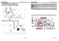
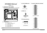
3. SETTING UP THE SYSTEM<br />
This section describes pin assignments for system’s external connectors and the jumpers setting.<br />
• Overview<br />
• System Setting<br />
3.1 OVERVIEW<br />
The AR-B1375 and AR-B1376 are all-in-one half size, Pentium single <strong>CPU</strong> board. This section provides<br />
hardware’s jumpers setting, the connectors’ locations, and the pin assignment.<br />
CAUTION: The <strong>CPU</strong> board doesn’t support the type DRAM SIMM of two-sided, it only supports single side DRAM<br />
SIMM.<br />
J11<br />
H9<br />
J1 J8<br />
CN4<br />
CN5<br />
CN6<br />
H4<br />
JP4<br />
1 1<br />
JP7<br />
J9<br />
CN7<br />
LED2<br />
J6<br />
1<br />
P5 P4 P2 P3P1 P6 H5<br />
U12<br />
CN8<br />
105<br />
JP6<br />
1<br />
H6<br />
1<br />
1<br />
2<br />
LED1<br />
CN9<br />
J2<br />
J3<br />
SIMM1<br />
SIMM2<br />
U3<br />
M1<br />
1<br />
2<br />
3<br />
A B C A B C A B C<br />
1 1<br />
2 2<br />
3 3<br />
U31<br />
M2<br />
MEM1<br />
M3<br />
U34<br />
2<br />
1<br />
JP5<br />
DB1<br />
1<br />
JP3<br />
U32<br />
MEM2<br />
U10<br />
LED3<br />
J7<br />
1<br />
H11 H10<br />
BUS2<br />
J5<br />
1<br />
2<br />
1<br />
1<br />
JP1<br />
JP2<br />
SW1<br />
CN2<br />
H8<br />
U33 MEM3<br />
CN1<br />
BUS1<br />
U11<br />
H7<br />
J10<br />
J4<br />
DB2<br />
CN3<br />
Figure 3-1 AR-B1376 Jumpers & Connectors Placement<br />
3-1
AR-B1375/AR-B1376 Users <strong>Guide</strong><br />
3.2 SYSTEM SETTING<br />
Jumper pins allow you to set specific system parameters. Set them by changing the pin location of jumper blocks.<br />
(A jumper block is a small plastic-encased conductor [shorting plug] that slips over the pins.) To change a jumper<br />
setting, remove the jumper from its current location with your fingers or small needle-nosed pliers. Place the<br />
jumper over the two pins designated for the desired setting. Press the jumper evenly onto the pins. Be careful not<br />
to bend the pins.<br />
We will show the locations of the AR-B1375 and AR-B1376 jumper pins, and the factory-default setting.<br />
CAUTION: Do not touch any electronic component unless you are safely grounded. Wear a grounded wrist strap<br />
or touch an exposed metal part of the system unit chassis. The static discharges from your fingers can<br />
permanently damage electronic components.<br />
3.2.1 Keyboard Connector<br />
(1) 6-Pin Mini DIN Keyboard Connector (CN3)<br />
CN3 is a Mini-DIN 6-pin connector. This keyboard connector is PS/2 type keyboard connector. This connector is<br />
also for a standard IBM-compatible keyboard with the keyboard adapter cable.<br />
CN3<br />
1 DATA<br />
2 N.C.<br />
3 GND<br />
4 VCC<br />
5 CLOCK<br />
6 N.C.<br />
1 2<br />
3 4<br />
5 6<br />
Front View<br />
Figure 3-2 CN3: 6-Pin Mini Din Keyboard Connector<br />
(2) AUX. Keyboard Connector (J4)<br />
We can use a PC/AT compatible keyboard to connecting the provided adapter cable between J4 and the keyboard.<br />
The pin assignments of J4 connector are as follows:<br />
1 CLOCK<br />
2 DATA<br />
3 N.C.<br />
4 GND<br />
5 VCC<br />
J4<br />
Figure 3-3 J4: AUX. Keyboard Connector<br />
3-2
AR-B1375/AR-B1376 Users <strong>Guide</strong><br />
3.2.2 PC/104 Connector<br />
(1) 40-Pin PC/104 Connector Bus C & D (CN1)<br />
1<br />
39<br />
2<br />
40<br />
40 Pin PC/104 Connector<br />
Figure 3-4 CN1: 40-Pin PC/104 Connector Bus C & D<br />
GND ---<br />
-SBHE ---<br />
LA23 ---<br />
LA22 ---<br />
LA21 ---<br />
LA20 ---<br />
LA19 ---<br />
LA18 ---<br />
LA17 ---<br />
-MEMR ---<br />
-MEMW ---<br />
SD8 ---<br />
SD9 ---<br />
SD10 ---<br />
SD11 ---<br />
SD12 ---<br />
SD13 ---<br />
SD14 ---<br />
SD15 ---<br />
Not Used ---<br />
(2) 64-Pin PC/104 Connector Bus A & B (CN2)<br />
C1<br />
C2<br />
C3<br />
C4<br />
C5<br />
C6<br />
C7<br />
C8<br />
C9<br />
C10<br />
C11<br />
C12<br />
C13<br />
C14<br />
C15<br />
C16<br />
C17<br />
C18<br />
C19<br />
C20<br />
CN1<br />
1 2<br />
D1 --- GND<br />
D2 --- -MEM16<br />
D3 --- -IO16<br />
D4 --- IRQ10<br />
D5 --- IRQ11<br />
D6 --- IRQ12<br />
D7 --- IRQ15<br />
D8 --- IRQ14<br />
D9 --- -DACK0<br />
D10 --- DRQ0<br />
D11 --- -DACK5<br />
D12 --- DRQ5<br />
D13 --- -DACK6<br />
D14 --- DRQ6<br />
D15 --- -DACK7<br />
D16 --- DRQ7<br />
D17 --- +5 VDC<br />
D18 --- -MASTER<br />
D19 --- GND<br />
D20 --- GND<br />
Figure 3-5 CN1: 40-Pin PC/104 Connector Bus C & D<br />
2<br />
64<br />
1<br />
63<br />
64-Pin PC/104 Connector<br />
Figure 3-6 CN2: 64 Pin PC/104 Connector Bus A & B<br />
-IOCHCK ---<br />
SD7 ---<br />
SD6 ---<br />
SD5 ---<br />
SD4 ---<br />
SD3 ---<br />
SD2 ---<br />
SD1 ---<br />
SD0 ---<br />
IOCHRDY---<br />
AEN ---<br />
SA19 ---<br />
SA18 ---<br />
SA17 ---<br />
SA16 ---<br />
SA15 ---<br />
SA14 ---<br />
SA13 ---<br />
SA12 ---<br />
SA11 ---<br />
SA10 ---<br />
SA9 ---<br />
SA8 ---<br />
SA7 ---<br />
SA6 ---<br />
SA5 ---<br />
SA4 ---<br />
SA3 ---<br />
SA2 ---<br />
SA1 ---<br />
SA0 ---<br />
GND ---<br />
A1<br />
A2<br />
A3<br />
A4<br />
A5<br />
A6<br />
A7<br />
A8<br />
A9<br />
A10<br />
A11<br />
A12<br />
A13<br />
A14<br />
A15<br />
A16<br />
A17<br />
A18<br />
A19<br />
A20<br />
A21<br />
A22<br />
A23<br />
A24<br />
A25<br />
A26<br />
A27<br />
A28<br />
A29<br />
A30<br />
A31<br />
A32<br />
CN2<br />
1 2<br />
B1<br />
B2<br />
B3<br />
B4<br />
B5<br />
B6<br />
B7<br />
B8<br />
B9<br />
B10<br />
B11<br />
B12<br />
B13<br />
B14<br />
B15<br />
B16<br />
B17<br />
B18<br />
B19<br />
B20<br />
B21<br />
B22<br />
B23<br />
B24<br />
B25<br />
B26<br />
B27<br />
B28<br />
B29<br />
B30<br />
B31<br />
B32<br />
--- GND<br />
--- RSTDRV<br />
--- +5 VDC<br />
--- IRQ9<br />
--- -5 VDC<br />
--- DRQ2<br />
--- -12 VDC<br />
--- -ZWS<br />
--- +12 VDC<br />
--- Not Used<br />
--- -SMEMW<br />
--- -SMEMR<br />
--- -IOW<br />
--- -IOR<br />
--- -DACK3<br />
--- DRQ3<br />
--- -DACK1<br />
--- DRQ1<br />
--- -REFRSH<br />
--- BUSCLK<br />
--- IRQ7<br />
--- IRQ6<br />
--- IRQ5<br />
--- IRQ4<br />
--- IRQ3<br />
--- -DACK2<br />
--- TC<br />
--- BALE<br />
--- +5 VDC<br />
--- OSC<br />
--- GND<br />
--- GND<br />
Figure 3-7 CN2: 64-Pin PC/104 Connector Bus A & B<br />
3-3
AR-B1375/AR-B1376 Users <strong>Guide</strong><br />
(3) I/O Channel Signal Description<br />
Name<br />
Description<br />
BUSCLK [Output] The BUSCLK signal of the I/O channel is asynchronous to<br />
the <strong>CPU</strong> clock.<br />
RSTDRV [Output] This signal goes high during power-up, low line-voltage or<br />
hardware reset<br />
SA0 - SA19 The System Address lines run from bit 0 to 19. They are<br />
[<strong>In</strong>put / Output] latched onto the falling edge of "BALE"<br />
LA17 - LA23 The Unlatched Address line run from bit 17 to 23<br />
[<strong>In</strong>put/Output]<br />
SD0 - SD15 System Data bit 0 to 15<br />
[<strong>In</strong>put/Output]<br />
BALE [Output] The Buffered Address Latch Enable is used to latch SA0 -<br />
SA19 onto the falling edge. This signal is forced high<br />
during DMA cycles<br />
-IOCHCK [<strong>In</strong>put] The I/O Channel Check is an active low signal which<br />
indicates that a parity error exist on the I/O board<br />
IOCHRDY<br />
This signal lengthens the I/O, or memory read/write cycle,<br />
[<strong>In</strong>put, Open collector] and should be held low with a valid address<br />
IRQ 3-7, 9-12, 14, 15 The <strong>In</strong>terrupt Request signal indicates I/O service request<br />
[<strong>In</strong>put] attention. They are prioritized in the following sequence :<br />
(Highest) IRQ 9, 10, 11, 12, 13, 15, 3, 4, 5, 6, 7 (Lowest)<br />
-IOR<br />
The I/O Read signal is an active low signal which instructs<br />
[<strong>In</strong>put/Output] the I/O device to drive its data onto the data bus<br />
-IOW [<strong>In</strong>put/Output] The I/O write signal is an active low signal which instructs<br />
the I/O device to read data from the data bus<br />
-SMEMR [Output] The System Memory Read is low while any of the low 1<br />
mega bytes of memory are being used<br />
-MEMR<br />
The Memory Read signal is low while any memory location<br />
[<strong>In</strong>put/Output] is being read<br />
-SMEMW [Output] The System Memory Write is low while any of the low 1<br />
mega bytes of memory is being written<br />
-MEMW<br />
The Memory Write signal is low while any memory location<br />
[<strong>In</strong>put/Output] is being written<br />
DRQ 0-3, 5-7 [<strong>In</strong>put] DMA Request channels 0 to 3 are for 8-bit data transfers.<br />
DMA Request channels 5 to 7 are for 16-bit data transfers.<br />
DMA request should be held high until the corresponding<br />
DMA has been completed. DMA request priority is in the<br />
following sequence:(Highest) DRQ 0, 1, 2, 3, 5, 6, 7<br />
(Lowest)<br />
-DACK 0-3, 5-7 The DMA Acknowledges 0 to 3, 5 to 7 are the<br />
[Output] corresponding acknowledge signals for DRQ 0 to 3 and 5<br />
to 7<br />
AEN [output] The DMA Address Enable is high when the DMA controller<br />
is driving the address bus. It is low when the <strong>CPU</strong> is driving<br />
the address bus<br />
-REFRESH This signal is used to indicate a memory refresh cycle and<br />
[<strong>In</strong>put/Output] can be driven by the microprocessor on the I/O channel<br />
TC [Output] Terminal Count provides a pulse when the terminal count<br />
for any DMA channel is reached<br />
SBHE [<strong>In</strong>put/Output] The System Bus High Enable indicates the high byte SD8 -<br />
SD15 on the data bus<br />
3-4
AR-B1375/AR-B1376 Users <strong>Guide</strong><br />
Name<br />
Description<br />
-MASTER [<strong>In</strong>put] The MASTER is the signal from the I/O processor which<br />
gains control as the master and should be held low for a<br />
maximum of 15 microseconds or system memory may be<br />
lost due to the lack of refresh<br />
-MEMCS16 The Memory Chip Select 16 indicates that the present data<br />
[<strong>In</strong>put, Open collector] transfer is a 1-wait state, 16-bit data memory operation<br />
-IOCS16<br />
The I/O Chip Select 16 indicates that the present data<br />
[<strong>In</strong>put, Open collector] transfer is a 1-wait state, 16-bit data I/O operation<br />
OSC [Output] The Oscillator is a 14.31818 MHz signal used for the color<br />
graphic card<br />
-ZWS<br />
The Zero Wait State indicates to the microprocessor that<br />
[<strong>In</strong>put, Open collector] the present bus cycle can be completed without inserting<br />
additional wait cycle<br />
Table 3-9 I/O Channel Signal’s Description<br />
3.2.3 Hard Disk (IDE) Connector (CN4)<br />
A 40-pin header type connector (CN4) is provided to interface with up to two embedded hard disk drives (IDE AT<br />
bus). This interface, through a 40-pin cable, allows the user to connect up to two drives in a “daisy chain” fashion.<br />
To enable or disable the hard disk controller, please use BIOS Setup program to select. The following table<br />
illustrates the pin assignments of the hard disk drive’s 40-pin connector.<br />
1<br />
2<br />
Figure 3-8 CN4: Hard Disk (IDE) Connector<br />
Pin Signal Pin Signal<br />
1 -RESET 2 GROUND<br />
3 DATA 7 4 DATA 8<br />
5 DATA 6 6 DATA 9<br />
7 DATA 5 8 DATA 10<br />
9 DATA 4 10 DATA 11<br />
11 DATA 3 12 DATA 12<br />
13 DATA 2 14 DATA 13<br />
15 DATA 1 16 DATA 14<br />
17 DATA 0 18 DATA 15<br />
19 GROUND 20 NOT USED<br />
21 NOT USED 22 GROUND<br />
23 -IOW 24 GROUND<br />
25 -IOR 26 GROUND<br />
27 -IORDY 28 BALE<br />
29 NOT USED 30 GROUND<br />
31 IRQ 14 32 -IOCS16<br />
33 SA 1 34 NOT USED<br />
35 SA 0 36 SA 2<br />
37 -CS 0 38 -CS 1<br />
39 HD LED 40 GROUND<br />
Table 3-1 HDD Pin Assignment<br />
3-5
AR-B1375/AR-B1376 Users <strong>Guide</strong><br />
3.2.4 FDD Port Connector (CN5)<br />
The AR-B1375 and AR-B1376 provide a 34-pin header type connector for supporting up to two floppy disk drives.<br />
1<br />
2<br />
Figure 3-9 CN5: FDD Port Connector<br />
Pin Signal Pin Signal<br />
1-33(odd) GROUND 18 DIRECTION<br />
2 -REDUCED WRITE<br />
CURRENT<br />
20 -STEP OUTPUT PULSE<br />
4 NOT USED 22 -WRITE DATA<br />
6 NOT USED 24 -WRITE ENABLE<br />
8 -INDEX 26 -TRACK 0<br />
10 -MOTOR ENABLE A 28 -WRITE PROTECT<br />
12 -DRIVE SELECT B 30 -READ DATA<br />
14 -DRIVE SELECT A 32 -SIDE 1 SELECT<br />
16 -MOTOR ENABLE B 34 DISK CHANGE<br />
Table 3-1 FDD Pin Assignment<br />
3.2.5 Parallel Port Connector (CN6)<br />
To use the parallel port, an adapter cable has connected to the CN6 (26-pin header type) connector. This adapter<br />
cable is mounted on a bracket and is included in your AR-B1375 or AR-B1376 package. The connector for the<br />
parallel port is a 25 pin D-type female connector.<br />
Parallel Port Connector<br />
1<br />
2<br />
13<br />
1<br />
25<br />
DB-25<br />
14<br />
D-Type Connector<br />
Figure 3-10 CN6: Parallel Port Connector<br />
CN6 DB-25 Signal CN6 DB-25 Signal<br />
1 1 -Strobe 2 14 -Auto Form Feed<br />
3 2 Data 0 4 15 -Error<br />
5 3 Data 1 6 16 -<strong>In</strong>itialize<br />
7 4 Data 2 8 17 -Printer Select <strong>In</strong><br />
9 5 Data 3 10 18 Ground<br />
11 6 Data 4 12 19 Ground<br />
13 7 Data 5 14 20 Ground<br />
15 8 Data 6 16 21 Ground<br />
17 9 Data 7 18 22 Ground<br />
19 10 -Acknowledge 20 23 Ground<br />
21 11 Busy 22 24 Ground<br />
23 12 Paper 24 25 Ground<br />
25 13 Printer Select 26 -- No Connect<br />
Table 3-1 Parallel Port Pin Assignment<br />
3-6
AR-B1375/AR-B1376 Users <strong>Guide</strong><br />
3.2.6 Serial Port<br />
(1) RS-232/RS-485 Select for COM-B (JP2)<br />
JP2 select the on-board RS-232/RS-485 for COM B, if choose RS-232 connecting with CN7; if choose RS-485<br />
connecting with J9.<br />
JP2<br />
1 2 3 1 2 3<br />
RS-232C RS-485<br />
(Factory Preset)<br />
(2) RS-485 Terminator (JP7)<br />
Figure 3-11 JP2: RS-232/RS-485 Select for COM-B<br />
JP7<br />
1 2 1 2<br />
OFF ON<br />
Factory Preset<br />
Figure 3-12 JP7: RS-485 Terminator<br />
(3) External RS-485 Adapter Select (J6 & J7)<br />
J6 and J7 can be set independently. J7 selects COM A port and J6 selects COM A port. J6 selects the external<br />
RS-485 for COM B connecting with CN7. J7 selects the external RS-485 for COM A connecting with DB2.<br />
J6 & J7<br />
1 2 3 1 2 3<br />
External RS-485 Adapter RS-232C<br />
(Factory Preset)<br />
Figure 3-13 J6 & J7: External RS-485 Adapter Select<br />
(4) RS-485 Header (J9)<br />
J9 is on-board RS-485 header. J9 pin assignments are as follows:<br />
1 N485+<br />
2 N485-<br />
3 GND<br />
J9 (COM B)<br />
1 2 3<br />
Figure 3-14 J9: RS-485 Header<br />
3-7
AR-B1375/AR-B1376 Users <strong>Guide</strong><br />
(5) RS-232 Connector (CN7 & DB2)<br />
There are two serial ports with EIA RS-232 interface on the AR-B1375 or AR-B1376. COM A uses one on-board<br />
D-type 9-pin male connector (DB2) which is located at the right side of the card, and COM B uses one 10-pin<br />
header (CN7) which is located at the upper of the card. To configure these two serial ports, use the BIOS Setup<br />
program to do well, and adjust the jumpers on J6 and J7.<br />
The pin assignments of the DB2 and CN7 for serial port A & B are as follows:<br />
DB2 (COM A)<br />
CN7 (COM B)<br />
GND 5<br />
1<br />
9-RI<br />
-DTR 4<br />
2<br />
8-CTS<br />
TXD 3<br />
7-RTS<br />
RXD 2<br />
6-DSR<br />
-DCD 1<br />
Figure 3-15 CN7 & DB2: RS-232 Connector<br />
CN7 DB2 Signal CN7 DB2 Signal<br />
1 1 -DCD 2 6 -DSR<br />
3 2 RXD 4 7 -RTS<br />
5 3 TXD 6 8 -CTS<br />
7 4 -DTR 8 9 -RI<br />
9 5 GND 10 -- Not Used<br />
Table 3-2 Serial Port Pin Assignment<br />
3.2.7 Reset Header (J1)<br />
J1 is used to connect to an external reset switch. Shorting these two pins will reset the system.<br />
1 Reset+<br />
2 Reset-<br />
Figure 3-16 J1: Reset Header<br />
3.2.8 LED Header<br />
(1) External Power LED Header (J2)<br />
(2) HDD LED Header (J8)<br />
1 2 3<br />
1 Power LED+<br />
2 No Connect<br />
3 Power LED-<br />
Figure 3-17 J2: External Power LED Header<br />
1 LED+<br />
2 LED-<br />
Figure 3-18 J8: HDD LED Header<br />
3-8
AR-B1375/AR-B1376 Users <strong>Guide</strong><br />
(3) Watchdog LED Header (J10)<br />
3.2.9 Power Connector (J3)<br />
J3 is 8-pin power connector, you can directly connect the power supply to the on board power connector for stand<br />
alone applications.<br />
1<br />
2<br />
3<br />
4<br />
5<br />
6<br />
7<br />
8<br />
GND<br />
+5 VDC<br />
+5 VDC<br />
GND<br />
GND<br />
+12 VDC<br />
-12 VDC<br />
-5 VDC<br />
Figure 3-20 J3: 8-Pin Power Connector<br />
3.2.10 External Speaker Header (J5)<br />
Besides the on board buzzer, you can use an external speaker by connecting J5 header directly.<br />
1 LED+<br />
2 LED-<br />
Figure 3-19 J10: Watchdog LED Header<br />
1 Speaker+<br />
2 Speaker-<br />
3 Speaker-<br />
4 Speaker-<br />
Figure 3-21 J5: External Speaker Header<br />
3.2.11 External Battery<br />
(1) Battery Charger Select (JP3)<br />
JP3<br />
1 2 3 1 2 3<br />
Rechargerable Non-Rechargerable<br />
(Factory Preset)<br />
Figure 3-22 JP3: Battery Charger Select<br />
3-9
AR-B1375/AR-B1376 Users <strong>Guide</strong><br />
(2) External Battery Connector (J11)<br />
J11 allows users to connector an external 4.5 to 6 VDC battery to the AR-B1375 and AR-B1376 if the on-board<br />
battery is fully discharged. The SRAM disk will draw the battery current. The battery charger on AR-B1375 and<br />
AR-B1376 doesn’t source charge current to the external battery, which connects to J11.<br />
1 Battery+<br />
2 Battery-<br />
1 2<br />
Figure 3-23 J11: External Battery Connector<br />
3.2.12 <strong>CPU</strong> Base Clock Select (JP1)<br />
The <strong>CPU</strong> base clock (<strong>In</strong>put clock) is twice of its operation clock.<br />
2<br />
1<br />
4<br />
3<br />
2<br />
1<br />
4<br />
3<br />
2<br />
1<br />
4<br />
3<br />
50MHz 80MHz 66.67MHz<br />
Factory Preset<br />
Figure 3-24 JP1: <strong>CPU</strong> Base Clock Select<br />
3.2.13 DRAM Configuration<br />
There is two 32-bit memory banks on the AR-B1375/AR-B1376 board. It can only put one-side DRAM SIMM to<br />
SIMM Socket (Single-Line Memory Modules), which is designed to accommodate 256KX36 bit to 4MX36-SIMMs.<br />
This provides the user with up to 32MB of main memory. The 32-bit SIMM (without parity bit) also can be used on<br />
AR-B1375/AR-B1376 board. There are six on-board memory configurations available. Please refer to the<br />
following table for details:<br />
SIMM1 SIMM2 Total Memory<br />
256KX32 (X36) None 1MB<br />
256KX32 (X36) 256KX32 (X36) 2MB<br />
256KX32 (X36) 1MX32 (X36) 5MB<br />
256KX32 (X36) 4MX32 (X36) 17MB<br />
1MX32 (X36) None 4MB<br />
1MX32 (X36) 256KX32 (X36) 5MB<br />
1MX32 (X36) 1MX32 (X36) 8MB<br />
1MX32 (X36) 4MX32 (X36) 20MB<br />
4MX32 (X36) None 16MB<br />
4MX32 (X36) 256KX32 (X36) 17MB<br />
4MX32 (X36) 1MX32 (X36) 20MB<br />
4MX32 (X36) 4MX32 (X36) 32MB<br />
Table 3-3 DRAM Configuration<br />
3-10
AR-B1375/AR-B1376 Users <strong>Guide</strong><br />
4. CRT/LCD FLAT PANEL DISPLAY<br />
This section describes the configuration and installation procedure using LCD and CRT display.<br />
• Connecting the CRT Monitor<br />
• LCD Flat Panel Display<br />
• Supported LCD Panel<br />
4.1 CONNECTING THE CRT MONITOR<br />
4.1.1 VGA Setting (JP5)<br />
(1) IRQ 9 Used Select<br />
JP5:Pin 1-2 Selecting IRQ 9<br />
2<br />
4<br />
2<br />
4<br />
1<br />
3<br />
1<br />
3<br />
Disabled Enabled<br />
Factory preset<br />
Figure 4-1 JP5: IRQ 9 Used Select<br />
(2) Zero Wait State<br />
JP5:Pin 3-4 Selecting ZWS<br />
2<br />
4<br />
2<br />
4<br />
1<br />
3<br />
1<br />
3<br />
Disabled Enabled<br />
Factory preset<br />
Figure 4-2 JP5: Zero Wait State (ZWS)<br />
4-1
AR-B1375/AR-B1376 Users <strong>Guide</strong><br />
4.1.2 CRT Connector (DB1)<br />
DB1 is used to connect with a VGA monitor when you are using the on-board VGA controller as display adapter. Pin<br />
assignments for the DB1 connector is as follows:<br />
NOTE: DB1 on the AR-B1375 is not functional. Its function is always used on the AR-B1376 <strong>CPU</strong> board.<br />
DB1 (CRT Connector)<br />
6<br />
1<br />
2<br />
3<br />
4<br />
5<br />
11<br />
15<br />
1 Red<br />
2 Green<br />
3 Blue<br />
13 Horizontial Sync<br />
14 Vertical Sync<br />
4, 9, 11, 12, & 15 Not Used<br />
5 & 10 Ground<br />
6, 7 & 8 AGND<br />
4.2 LCD FLAT PANEL DISPLAY<br />
10<br />
Figure 4-1 DB1: CRT Connector<br />
This section describes the configuration and installation procedure for a LCD display. Skip this section if you are<br />
using a CRT monitor only.<br />
Using the Flash Memory Writer utility to download the new BIOS file into the ROM chip to configure the BIOS<br />
default setting for different types of LCD panel. And then set your system properly and configure the AR-B1376<br />
VGA module for the right type of LCD panel you are using.<br />
If you are using a different LCD panel other than those listed, choose from the panel description column which type<br />
of LCD panel you are using.<br />
The following shows the block diagram of using AR-B1376 for LCD display.<br />
AR-B1376<br />
<strong>CPU</strong> Boad<br />
LCD<br />
Panel<br />
VBL Control<br />
+12V, +5V<br />
VEE<br />
<strong>In</strong>verter<br />
Board<br />
FL HIGH<br />
Voltage<br />
Figure 4-2 LCD Panel Block Diagram<br />
The block diagram shows that the AR-B1376 still needs components to be used for LCD panel. The inverter board<br />
provides the control for the brightness and the contrast of the LCD panel while the inverter is the one that supplies<br />
the high voltage to drive the LCD panel. Each item will be explained further in the section.<br />
4-2
AR-B1375/AR-B1376 Users <strong>Guide</strong><br />
Pin 1<br />
<strong>In</strong>verter & Contrast<br />
CN9<br />
CN8<br />
AR-B1376<br />
<strong>CPU</strong> Board<br />
LCD<br />
Panel<br />
Pin 1<br />
Figure 4-3 LCD Panel Cable <strong>In</strong>stallation Diagram<br />
NOTE: Be careful with the pin orientation when installing connectors and the cables. A wrong connection can easily<br />
destroy your LCD panel. Pin 1 of the cable connector is indicated with a sticker and pin1 of the ribbon<br />
cable is usually has a different color.<br />
4.2.1 <strong>In</strong>verter Board Description<br />
The inverter board is the one that supplies the high voltage signals to drive the LCD panel by converting the 12 volt<br />
signal from the AR-B1376 into high voltage AC signal for LCD panel. It can be installed freely on the space<br />
provided over the VR board. If the VR board is installed on the bracket, you have to provide a place to install the<br />
inverter board into your system.<br />
4.2.2 LCD Connector<br />
The AR-B1376 supports CRT colored monitor, STN, Dual-Scan, TFT, monochrome and color panels. It can be<br />
connected to create a compact video solution for the industrial environment. 1MB of RAM on-boarded allows a<br />
maximum CRT resolution of 1024X768 and a LCD resolution of 640X480 with 64K colors. For different VGA<br />
display modes, your monitor must possess certain characteristics to display the mode you want.<br />
(1) DE/E Signal from M or LP Select (JP6)<br />
JP6<br />
1 2 3 1 2 3<br />
DE/M<br />
E/LP<br />
(Factory Preset)<br />
Figure 4-4 JP6: DE/E Signal from M or LP Select<br />
(2) LCD Control Connector (CN9)<br />
CN9 is a 5-pin connector that attaches to the Contrast and Backlight board; its pin assignment is shown below:<br />
NOTE: AR-B1375 doesn’t provide this function.<br />
1 ENABLK<br />
2 ENVEE<br />
3 +12V<br />
4 GND<br />
5 VEE<br />
Figure 4-5 CN9: LCD Control Connector<br />
4-3
AR-B1375/AR-B1376 Users <strong>Guide</strong><br />
(3) LCD Panel Display Connector (CN8)<br />
Attach a display panel connector to this 44-pin connector with pin assignments as shown below:<br />
NOTE: AR-B1375 doesn’t provide this function.<br />
Figure 4-6 CN8: LCD Display Connector<br />
1<br />
2<br />
Pin Signal Pin Signal<br />
1 GND 2 SHFCLK<br />
3 GND 4 LP<br />
5 FLM 6 GND<br />
7 P0(B0) 8 P1(B1)<br />
9 P2(B2) 10 P3(B3)<br />
11 P4(B4) 12 P5(B5)<br />
13 GND 14 P6(B6)<br />
15 P7(B7) 16 P8(G0)<br />
17 P9(G1) 18 P10(G2)<br />
19 P11(G3) 20 GND<br />
21 P12(G4) 22 P13(G5)<br />
23 P14(G6) 24 P15(G7)<br />
25 P16(R0) 26 P17(R1)<br />
27 GND 28 P18(R2)<br />
29 P19(R3) 30 P20(R4)<br />
31 P21(R5) 32 P22(R6)<br />
33 P23(R7) 34 GND<br />
35 VCC 36 VCC<br />
37 +12V 38 +12V<br />
39 GND 40 GND<br />
41 DE 42 ENABLK<br />
43 GND 44 VEE<br />
Table 4-4 LCD Display Assignment<br />
4.3 SUPPORTED LCD PANEL<br />
At present, this VGA card can provide a solution with an inverter board for the following list of standard LCD<br />
panels. Consult your Acrosser representative for new developments. When using other models of standard LCD<br />
panels in the market.<br />
NO. Manufacture Model No. Description<br />
1 NEC NL-6448AC30-10 TFT 9.4”<br />
2 NEC NL-6448AC32-10 TFT 10.2”<br />
3 NEC NL-6448AC33-10 TFT 10.4”<br />
4 HITACHI LMG5371 MONO 9.4” Dual Scan<br />
5 HITACHI LMG9200 DSTN 9.4”<br />
6 HITACHI LMG9400 DSTN 10.4”<br />
7 ORION OGM-640CN03C-S DSTN 10.4”<br />
8 SHARP LQ10D321 TFT 10.4”<br />
Table 4-5 LCD Panel Type List<br />
CAUTION: 1. If you want to connect the LCD panel, you must update the AR-B1376’s BIOS, then you can setup<br />
the corrected BIOS. Please contact Acrosser for the latest BIOS update.<br />
2. If user needs to update the BIOS version or connect other LCD, please contact the sales department.<br />
The detail supported LCDs are listed in the Acrosser Web site, user can download the suitable BIOS.<br />
The address is as follows:<br />
http:\\www.acrosser.com<br />
4-4
AR-B1375/AR-B1376 Users <strong>Guide</strong><br />
5. INSTALLATION<br />
This chapter describes the procedure of the utility diskette installation. The following topics are covered:<br />
5.1 OVERVIEW<br />
• Overview<br />
• Utility Diskette<br />
• Write Protect Function<br />
• Watchdog Timer<br />
This chapter provides information for you to set up a working system based on the AR-B1375/AR-B1376 <strong>CPU</strong> card.<br />
Please read the details of the <strong>CPU</strong> card’s hardware descriptions before installation carefully, especially jumpers’<br />
settings, switch settings and cable connections.<br />
Follow steps listed below for proper installation:<br />
Step 1 :<br />
Step 2 :<br />
Step 3 :<br />
Step 4 :<br />
Step 5 :<br />
Step 6 :<br />
Step 7 :<br />
Step 8 :<br />
Step 9 :<br />
Step 10:<br />
Step 11:<br />
Step 12:<br />
Read the <strong>CPU</strong> card’s hardware description in this manual.<br />
<strong>In</strong>stall any DRAM SIMM onto the <strong>CPU</strong> card.<br />
Set jumpers.<br />
Make sure that the power supply connected to your passive <strong>CPU</strong> board back plane is turned off.<br />
Plug the <strong>CPU</strong> card into a free AT-bus slot or PICMG slot on the back plane and secure it in place<br />
with a screw to the system chassis.<br />
Connect all necessary cables. Make sure that the FDC, HDC, serial and parallel cables are<br />
connected to pin 1 of the related connector.<br />
Connect the hard disk/floppy disk flat cables from the <strong>CPU</strong> card to the drives. Connect a power<br />
source to each drive.<br />
Plug the keyboard into the keyboard connector.<br />
Turn on the power.<br />
Configure your system with the BIOS Setup program then re-boot your system.<br />
If the <strong>CPU</strong> card does not work, turn off the power and read the hardware description carefully again.<br />
If the <strong>CPU</strong> card still does not perform properly, return the card to your dealer for immediate service.<br />
5.2 UTILITY DISKETTE<br />
AR-B1376 provides two VGA driver diskettes, supports WIN31 & WIN95. If your operation system is the other<br />
operation system, please attach Acrosser that will provide the technical supporting for the VGA resolution.<br />
There are two diskettes: disk 1 is for WIN31 & MS-DOS VGA resolution; disk 2 is for WIN95 and SSD utility. Every<br />
diskette attach the README.* file. The AR-B1375 attached the SSD utility only, if you use the AR-B1375 skip the<br />
section of VGA driver. Please refer to the file of README for any troubleshooting before install the driver.<br />
5-1
AR-B1375/AR-B1376 Users <strong>Guide</strong><br />
5.2.1 VGA Driver<br />
(1) WIN 3.1 Driver<br />
For the WIN31 operation system, user must in the DOS mode decompress the compress file. And then as to the<br />
steps:<br />
Step 1:<br />
Step 2:<br />
Step 3:<br />
Step 4:<br />
Step 5:<br />
<strong>In</strong> the DOS mode execute the SETUP.EXE file.<br />
A:\>SETUP<br />
The screen shows the chip type, and press any key enter the main menu.<br />
There is 9 items for choice to setup. Please choose the item, notice the<br />
function key defined. Press [ENTER] selected the , when this line appears [*]<br />
symbol that means this item is selected. Press [End] starts to install.<br />
The screen will show the dialog box to demand user typing the WIN31’s path. The default is<br />
C:\WINDOWS.<br />
Follow the setup steps’ messages execute. As completed the setup procedure will generate the<br />
message as follow.<br />
<strong>In</strong>stallation is done!<br />
Change to your Windows directory and type SETUP to run the Windows Setup program. Choose<br />
one of the new drivers marked by an *. Please refer to the <strong>User’</strong>s <strong>Guide</strong> to complete the installation.<br />
Step 6:<br />
Step 7:<br />
Step 8:<br />
Press [Esc] key to return the main menu, and re-press [Esc] return to the DOS mode.<br />
User can enter the WIN31 so you can find the icon located in the {CONTROL PANEL}<br />
group.<br />
Adjust the , , , , and .<br />
(2) WIN 95 Driver<br />
For the WIN95 operating system, user must in the DOS mode decompress the compress file. And then as to the<br />
steps:<br />
Step 1:<br />
Step 2:<br />
Step 3:<br />
Enter the WIN95 operation system, please choose the item of the icon in<br />
the {CONTROL PANEL}. Please select the item, and type the factory source<br />
files’ path.<br />
A:\VGAW95<br />
And then you can find the item, select it and click the <br />
button.<br />
Finally, user can find the icon adds the item. You can select this item, and<br />
adjust the , , …and other functions. Please refer to<br />
the messages during installation.<br />
5-2
AR-B1375/AR-B1376 Users <strong>Guide</strong><br />
5.2.2 SSD Utility<br />
To support the AR-B1375/AR-B1376 solid-state disk’s operations, the following files have been provided on the<br />
enclosed diskette’s directory .<br />
(A) PGM137x.EXE<br />
PGM137x.EXE PGM137x.EXE is used to program the 12V FLASH EPROM after the ROM pattern files are<br />
generated by RFG.EXE. The PGM137x.EXE can also program the correctness of the ROM<br />
pattern files onto 5V FLASH EPROM (start from MEM1) or SRAM for testing the ROM pattern<br />
files.<br />
To execute PGM137x.EXE, the main menu will be displayed on your screen. There are 8 options on the main<br />
menu.<br />
Quit to DOS<br />
Quits and exits to the DOS.<br />
OS Shell<br />
Exits from PGM137x temporarily to the DOS prompt. Type EXIT to return to PGM137x main menu.<br />
Load ROM File<br />
If this option is used, the PGM137x will prompt you for the ROM pattern file name. This option is useful if<br />
you have not previously entered a ROM pattern file name or if you wish to use a different ROM pattern file.<br />
The PGM137x will check and display the ROM file name, ROM file size, (FLASH) memory capacity and the<br />
number of ROM pattern files that will be loaded and copied onto the (FLASH) memory chips.<br />
Verify Memory<br />
If ROM pattern files were loaded without error, this option instructs PGM137x to verify the contents of<br />
(FLASH) memory chips with the current ROM pattern files.<br />
Program Memory<br />
If there are no mistakes in your ROM pattern file, then this menu option will erase (FLASH) memory, write<br />
the current ROM pattern files onto (FLASH) memory and verify data that was just written to (FLASH)<br />
memory, using the ROM pattern files.<br />
Memory Type/Mfr.<br />
Before you program the (FLASH) memory chips, make sure that the FLASH’s type and manufactory match<br />
the one shown on the main menu. Otherwise, you can use this option to select the proper type and<br />
manufacture and instruct the program to use a right programming algorithm.<br />
Select PGM Chips<br />
Normally the PGM137x will program all ROM pattern files onto the FLASH memories with the ROM pattern<br />
files just loaded. But you can use this option to select which memory chips that you want to program and<br />
which memory chips need to be skipped. The PGM137x will only program the selected chips when writing<br />
data to the FLASH memory. This is very useful when some of the memory chip were verified and<br />
programmed previously.<br />
Select FLASH PLSCNTs<br />
If the 12V FLASHs have been programmed several times, please select the FLASH PLSCNT<br />
mode instead of mode. <strong>In</strong> the or mode, PGM137x.EXE will retry more<br />
times to program data onto the 12V FLASHs correctly. The default setting is mode.<br />
(B) WD137x.EXE<br />
WD137x.EXE This program demonstrates how to enable and trigger the watchdog timer. It allows you to<br />
test the function when the watchdog timer is enabled.<br />
5-3
AR-B1375/AR-B1376 Users <strong>Guide</strong><br />
(C) WP137x.EXE<br />
WP137x.EXE This program demonstrates how to enable and disable software write protected function. It<br />
also shows the current protect mode of write or read only memory.<br />
(D) RFG.EXE<br />
RFG.EXE<br />
This program is used to generate ROM pattern files in a binary format. Each ROM pattern file<br />
has the same size as the FLASH or EPROM and can be easily programmed on to the FLASH<br />
with on-board programmer or on to EPROM with any EPROM programmer. If you have<br />
specified a DOS drive in the *.PGF file, RFG will generate bootable ROM pattern files for the<br />
EPROM or FLASH disk. The RFG supports the following DOS:MS-DOS, PC-DOS, DR-DOS,<br />
and X-DOS.<br />
NOTE: If you want to use AR-B137x with any DOS, which is not supported by RFG, please send your requirement<br />
to Acrosser Technology Co., Ltd. or contract with your local sales representative.<br />
The RFG.EXE provided in the utility diskette is a program that converts the files you list in the PGF and convert<br />
them into ROM pattern file. The RFG will determine how many EPROMs are needed and generate the same<br />
number of ROM pattern files. These ROM pattern files are named with the name assigned by the ROM_NAME in<br />
the PGF and the extension names are *.R01, *.R02….etc. To generate ROM pattern files.<br />
The ROM File Generator main menu will be displayed on the screen. There are 7 options on the main menu. They<br />
serve the following functions:<br />
Quit to DOS<br />
Quits and exits to the DOS<br />
OS Shell<br />
Exits from the RFG temporarily to the DOS prompt. Type to return to the RFG main menu.<br />
Load PFG File<br />
If this option is used, the RFG will prompt you for the PGF file name. This option is useful if you have not<br />
previously entered a PGF name or you wish to use a different PGF file. The RFG will check and display the<br />
PGF filename, ROM pattern file name, EPROM capacity, DOS version and the number of ROM pattern files<br />
that will be generated.<br />
Type Current PGF File<br />
This option instructs the RFG to use the DOS type command to display the contents of the current PGF file.<br />
Generate ROM File(s)<br />
If there is no mistake in your *.PGF file, then this menu option will generate ROM pattern files. The number<br />
of ROM pattern file generated by the RFG will depend on the total capacity needed by your files. For<br />
instance, if 3 files are generated, then you will need to use 3 EPROMs (The size depends upon the number<br />
stated in your PGF). The ROM pattern files will have the same file names, but will have different extension<br />
names. For example:<br />
TEST.R01, TEST.R02, TEST.R03…etc.<br />
Display Error in PGF File<br />
This option displays errors that were detected in your PGF.<br />
Help to PGF File<br />
This option gives information on how to write a PGF file and how to generate ROM pattern files. An<br />
example PGF is also included.<br />
Move the reverse video bar to then press [ENTER]. The ROM pattern file is a<br />
binary file. The file size will be the same size as the EPROM that you assigned in the PGF. For example, if<br />
you are using 128KX8 EPROM memory chips, then the size of ROM patterns file will be 131072 bytes. For<br />
other chips the file size will be:<br />
64KX8 EPROM----65536 bytes<br />
256KX8 EPROM—262144 bytes<br />
512KX8 EPROM---524288 bytes<br />
1MX8 EPROM -----1048576 bytes<br />
5-4
AR-B1375/AR-B1376 Users <strong>Guide</strong><br />
(E) RFGDEMO.PGF<br />
RFGDEMO.PGF This file provides a sample PROGRAM GROUP FILE, which illustrates how to create ROM<br />
pattern files correctly.<br />
The PGF is an ASCII text file that can be created by using any text editor, word processor or DOS <br />
command. The PGF lists what files will be copied and if DOS is going to be copied. This file can have any DOS<br />
filename, but the extension name must be *.PGF. For example, followings are valid filenames.<br />
RFGDEMO.PGF<br />
MYRFG.PGF<br />
MSDOS.PGF<br />
….<br />
An examples of the *.PGF file is as follow.<br />
ROM_NAME=TEST1 ; ROM pattern file name is TEST1<br />
;The output file names will be TEST1.R01, TEST1.R02..etc.<br />
DOS_DRIVE=C: ; DOS system drive unit is drive C:<br />
;If user does not want to copy DOS<br />
;system files onto the ROM disk<br />
;write as DOS_DRIVE=NONE<br />
ROM_SIZE=128 ;128 means 128KX8 (27C/29F010) EPROM size used<br />
;256 means 512KX8 (27C/29F020) EPROM size used<br />
;512 means 512KX8 (27C/29F040) EPROM size used<br />
;1024 means 1MX8 (27C080) EPROM size used<br />
The following two files are options, which depend on whether the ROM disk is to be bootable, or not.<br />
CONFIG.SYS<br />
AUTOEXEC.BAT<br />
;Below are user’s files<br />
A:\USER1.COM ; File USER1.COM on root of drive A:<br />
USER2.EXE ; File USER2.EXE on current directory & drive<br />
C:\TTT\USER3.TXT ; File USER3.TXT on sub-directory TTT of drive C:<br />
5.3 WRITE PROTECT FUNCTION<br />
The AR-B1375 and AR-B1376 provide hardware and software write protect functions for small page 5V FLASH<br />
disk and only software write protected function for SRAM disk. This is to prevent your data on 5V FLASH or SRAM<br />
disk from accidental deletion or overwrite. If your FLASH/SRAM disk is write protected, any write operation to the<br />
protected FLASH/SRAM disk will get a write protect error:<br />
Write protect error writing drive A<br />
About, Retry, Fail?<br />
5-5
AR-B1375/AR-B1376 Users <strong>Guide</strong><br />
5.3.1 Hardware Write Protect<br />
To enable the hardware protect function for small page 5V FLASH disk, please refer to the “Switch Setting”.<br />
5.3.2 Software Write Protect<br />
If you need the write protect function and sometimes you have to write or update data on your FLASH/SRAM disk,<br />
you can use the software write protect instead of hardware write protect. The software writes protect function is<br />
enabled or disabled by writing a data to an I/O port.<br />
5.3.3 Enable the Software Write Protect<br />
Writes data 08h to the base port+0 address<br />
Example 1: (in assembly language)<br />
MOV DX, 210H ; If the base I/O address is 210H<br />
MOV AL, 80H ; Enable byte = 80h<br />
OUT DX, AL<br />
Example 2: (in BASICA language)<br />
OUT &H210, &H80; REM If the base I/O address is 210h<br />
Example 3: (in Turbo C language)<br />
Outportb (0x210, 0x80);/*If the base I/O address is 210h*/<br />
5.3.4 Disable the Software Write Protect<br />
Writes data 0 to the base port+0 address<br />
Example 1: (in assembly language)<br />
MOV DX, 210H ; If the base I/O address is 210h<br />
MOV AL, 00H ; Disable byte=00h<br />
OUT DX, AL<br />
Example 2: (in BASICA language)<br />
OUT &H210, &H00; REM If the base I/O address is 210h<br />
Example 3: (in Turbo C language)<br />
Outportb (0x210, 0x00);/*If the base I/O address is 210h*/<br />
5-6
AR-B1375/AR-B1376 Users <strong>Guide</strong><br />
5.4 WATCHDOG TIMER<br />
This section describes how to use the Watchdog Timer, disabled, enabled, and trigger.<br />
The AR-B1375/AR-B1376 is equipped with a programmable time-out period watchdog timer. User can use the<br />
program to enable the watchdog timer. Once you have enabled the watchdog timer, the program should trigger it<br />
every time before it times out. If your program fails to trigger or disable this timer before it times out because of<br />
system hang-up, it will generate a reset signal to reset the system. The time-out period can be programmed to be<br />
3 to 42 seconds.<br />
Enable (D7)<br />
Time Factor (D0-D2)<br />
Write and Trigger<br />
Watchdog<br />
Register<br />
Time Base<br />
Counter<br />
and<br />
Compartor<br />
Watchdog<br />
LED<br />
Figure 5-1 Watchdog Block Diagram<br />
RESET<br />
5.4.1 Watchdog Timer Setting<br />
The watchdog timer is a circuit that may be used from your program software to detect crashes or hang-ups.<br />
Whenever the watchdog timer is enabled, the LED will blink to indicate that the timer is counting. The watchdog<br />
timer is automatically disabled after reset.<br />
Once you have enabled the watchdog timer, your program must trigger the watchdog timer every time before it<br />
times-out. After you trigger the watchdog timer, it will be set to zero and start to count again. If your program fails<br />
to trigger the watchdog timer before time-out, it will generate a reset pulse to reset the system or trigger the IRQ15<br />
signal to tell your program that the watchdog is times out.<br />
The factor of the watchdog timer time-out constant is approximately 6 seconds. The period for the watchdog timer<br />
time-out period is between 1 to 7 timer factors.<br />
If you want to reset your system when watchdog times out, the following table listed the relation of timer factors<br />
between time-out periods.<br />
Time Factor<br />
Time-Out Period (Seconds)<br />
80H 3<br />
81H 6<br />
82H 12<br />
83H 18<br />
84H 24<br />
85H 30<br />
86H 36<br />
87H 42<br />
Table 5-1 Time-Out Setting<br />
If you want to generate IRQ15 signal to warn your program when watchdog times out, the following table listed the<br />
relation of timer factors between time-out period. And if you use the IRQ15 signal to warn your program when<br />
watchdog timer out, please enter the BIOS Setup the menu, the and these two items must set to Primary.<br />
Time Factor<br />
Time-Out Period (Seconds)<br />
0C0H 3<br />
0C1H 6<br />
0C2H 12<br />
0C3H 18<br />
0C4H 24<br />
0C5H 30<br />
0C6H 36<br />
0C7H 42<br />
Table 5-2 Time-Out Setting<br />
5-7
AR-B1375/AR-B1376 Users <strong>Guide</strong><br />
NOTE: 1. If you program the watchdog to generate IRQ15 signal when it times out, you should initial IRQ15<br />
interrupt vector and enable the second interrupt controller (8259 PIC) in order to enable <strong>CPU</strong> to process<br />
this interrupt. An interrupt service routine is required too.<br />
2. Before you initial the interrupt vector of IRQ15 and enable the PIC, please enable the watchdog timer<br />
previously, otherwise the watchdog timer will generate an interrupt at the time watchdog timer is enabled.<br />
5.4.2 Watchdog Timer Enabled<br />
To enable the watchdog timer, you have to output a byte of timer factor to the watchdog register whose address is<br />
214H or Base Port. The following is a BASICA program, which demonstrates how to enable the watchdog timer<br />
and set the time-out period at 24 seconds.<br />
1000 REM Points to command register<br />
1010 WD_REG% = 214H<br />
1020 REM Timer factor = 84H (or 0C4H)<br />
1030 TIMER_FACTOR% = %H84<br />
1040 REM Output factor to watchdog register<br />
1050 OUT WD_REG%, TIMER_FACTOR%<br />
.,etc.<br />
5.4.3 Watchdog Timer Trigger<br />
After you enable the watchdog timer, your program must write the same factor as enabling to the watchdog register<br />
at least once every time-out period to its previous setting. You can change the time-out period by writing another<br />
timer factor to the watchdog register at any time, and you must trigger the watchdog before the new time-out period<br />
in next trigger. Below is a BASICA program which demonstrates how to trigger the watchdog timer:<br />
2000 REM Points to command register<br />
2010 WD_REG% = 214H<br />
2020 REM Timer factor = 84H (or 0C4H)<br />
2030 TIMER_FACTOR% = &H84<br />
2040 REM Output factor to watchdog register<br />
2050 OUT WD_REG%, TIMER_FACTOR%<br />
.,etc.<br />
5.4.4 Watchdog Timer Disabled<br />
To disable the watchdog timer, simply write a 00H to the watchdog register.<br />
3000 REM Points to command register<br />
3010 WD_REG% = BASE_PORT%<br />
3020 REM Timer factor = 0<br />
3030 TIMER_FACTOR% = 0<br />
3040 REM Output factor to watchdog register<br />
3050 OUT WD_REG%, TIMER_FACTOR%<br />
., etc.<br />
5-8
1<br />
104<br />
105<br />
1<br />
104<br />
CN1<br />
81<br />
100<br />
1<br />
51<br />
50<br />
31<br />
1<br />
1<br />
AR-B1375/AR-B1376 Users <strong>Guide</strong><br />
6.SOLID STATE DISK<br />
The section describes the various type SSDs’ installation steps as follows. This chapter describes the procedure of<br />
the installation. The following topics are covered:<br />
6.1 OVERVIEW<br />
• Overview<br />
• Switch Setting<br />
• Jumper Setting<br />
• ROM Disk <strong>In</strong>stallation<br />
The AR-B1375 and AR-B1376 provides three 32-pin JEDEC DIP sockets, which may be populated with up to 3MB<br />
of EPROM or 1.5MB of FLASH or 1.5MB of SRAM disk. It is ideal for diskless systems, high reliability and/or high<br />
speed access applications, controller for industrial or line test instruments, and etc.<br />
If small page (less or equal 512 bytes per page) 5V FLASHs were used, you could format FLASH disk and copy<br />
files onto FLASH disk just like using a normal floppy disk. You can use all of the related DOS command (such as<br />
COPY, DEL…etc.) to update files on the 5V FLASH disk.<br />
The write protect function allows you to prevent your data on small page 5V FLASH or SRAM disk from accidental<br />
deletion or overwrite.<br />
An on-board Lithium battery or an external battery pack that could be connected ensures data retention of SRAM<br />
to the AR-B1375 and AR-B1376.<br />
6.2 SWITCH SETTING<br />
We will show the locations of the AR-B1375 and AR-B1376 switch, and the factory-default setting.<br />
CAUTION: The switch setting needs to adjust with the jumpers setting, make sure the jumper settings and the<br />
switch setting are correct.<br />
J11<br />
H9<br />
J1 J8<br />
CN4<br />
CN5<br />
CN6<br />
H4<br />
JP4<br />
1 1<br />
JP7<br />
CN7<br />
LED2<br />
J9<br />
J6<br />
1<br />
P5 P4 P2 P3P1 P6 H5<br />
U12<br />
CN8<br />
105<br />
JP6<br />
1<br />
H6<br />
1<br />
1<br />
2<br />
LED1<br />
CN9<br />
J2<br />
J3<br />
SIMM1<br />
SIMM2<br />
U3<br />
M1<br />
A B C A B C A B C<br />
1<br />
1 1<br />
2<br />
2 2<br />
3<br />
3 3<br />
M2<br />
U31 MEM1<br />
M3<br />
U34<br />
2<br />
1<br />
JP5<br />
DB1<br />
1<br />
JP3<br />
U32<br />
MEM2<br />
U10<br />
LED3<br />
J7<br />
1<br />
H11 H10<br />
BUS2<br />
J5<br />
1<br />
2<br />
1<br />
1<br />
JP1<br />
JP2<br />
SW1<br />
CN2<br />
H8<br />
U33 MEM3<br />
CN1<br />
BUS1<br />
U11<br />
H7<br />
J10<br />
J4<br />
DB2<br />
CN3<br />
Figure 6-1 Switch & SSD Type Jumper Location<br />
6-1
AR-B1375/AR-B1376 Users <strong>Guide</strong><br />
6.2.1 Overview<br />
There is 1 DIP Switch located on the AR-B1375 and AR-B1376. It performs the following functions:<br />
ON<br />
OFF<br />
1 2 3 4 5 6<br />
Figure 6-2 SW1: Switch Select<br />
SW1-1<br />
SW1-2<br />
SW1-3 & SW1-4<br />
SW1-5 & SW1-6<br />
Set the base I/O port address<br />
Set the starting memory address<br />
Set the drive number of solid state<br />
disk<br />
Set the used ROM memory chips<br />
6.2.2 I/O Port Address Select (SW1-1)<br />
SW1-1 is provided to select one of the four base port addresses for the watchdog timer and the solid state disk.<br />
The AR-B1375 and AR-B1376 occupy 6 I/O port addresses. Followings state selections of base port address.<br />
SW1-1 Base Port Solid State Disk Watchdog<br />
OFF (*) 210h 210h-213h 214h-215h<br />
ON 290h 290h-293h 294h-295h<br />
Table 6-1 I/O Port Address Select<br />
6.2.3 SSD Firmware Address Select (SW1-2)<br />
The AR-B1375‘s and AR-B1376’s SSD firmware occupies 8KB of memory. SW1-2 is used to select the memory<br />
base address. You must select an appropriate address so that the AR-B1375 or AR-B1376 will not conflict with<br />
memory installed on other add-on memory cards. Additionally, be sure not to use shadow RAM area or EMM<br />
driver’s page frame in this area.<br />
SW1-2<br />
Bank Memory Address<br />
OFF (*)<br />
C800:0 (8KB)<br />
ON<br />
D800:0 (8KB)<br />
Table 6-2 SSD Firmware Address Select<br />
If you are not going to use the solid state disk (SSD), you can use BIOS setup program to disable the SSD BIOS.<br />
The AR-B1375 or AR-B1376 will not occupy any memory address if the SSD BIOS is disabled.<br />
If you are going to install the EMM386.EXE driver, please use the [X] option to prevent EMM386.EXE from using<br />
the particular range of segment address as an EMS page which is used by AR-B1375/AR-B1376. For example,<br />
write a statement in the CONFIG.SYS file as follow: (If the memory configuration of AR-B1375/AR-B1376 is<br />
C800:0)<br />
DEVICE=C:\DOS\EMM386.EXE X=C800-C9FF<br />
6-2
AR-B1375/AR-B1376 Users <strong>Guide</strong><br />
6.2.4 SSD Drive Number (SW1-3 & SW1-4)<br />
The AR-B1375/AR-B1376’s SSD can simulate one or two disk drives. You can assign the drive letter of the AR-<br />
B1375/AR-B1376 by configuring SW1-3 & SW1-4.<br />
You can make the computer to boot from SSD by copying DOS into the SSD. If your SSD does not have DOS, the<br />
computer will boot from your hard disk or floppy disk. <strong>In</strong> this condition, the SSD BIOS of AR-B1375/AR-B1376 will<br />
set the drive letter of the SSD to the desired drive letter automatically.<br />
The SSD BIOS will simulate one disk drive when only (FLASH) EPROM or SRAM (starting from MEM1 socket) is<br />
installed. The drive numbers with respect to the switch setting when the AR-B1375/AR-B1376 simulates single<br />
disk drives.<br />
SW1-3 SW1-4 Occupies floppy disk number (SSD)<br />
OFF (*) OFF 0 or 1 (Note 1)<br />
ON OFF 0 or 2 (Note 2)<br />
OFF ON 0<br />
ON ON 0<br />
Table 6-3 SSD Drive Number<br />
NOTE: 1. If there is no DOS on this SSD, the disk number will 1 (B:). If any DOS is found by the AR-B1375/AR-<br />
B1376 SSD BIOS, the disk number will be 0 (A:) But, you can change the disk number from 0 to 1 by<br />
pressing the key during system bootup.<br />
2. If there is no DOS on this SSD, the disk number will be 2 (C: or D: or…). If any DOS is found by AR-<br />
B1375/AR-B1376 SSD BIOS, the disk number will be 0 (A:). But, you can change the disk number from<br />
0 to 2 by pressing the key during system bootup.<br />
(1) Simulate 2 Disk Drive<br />
When (FLASH) EPROM and SRAM are both used on the AR-B1375/AR-B1376, or you only have installed SRAM<br />
that does not start from MEM1 socket, the AR-B1375/AR-B1376 will simulate two disk drives. The drive numbers<br />
respect to those switch settings when AR-B1375/AR-B1376 simulates two disk drives.<br />
SW1-3 SW1-4<br />
Occupies floppy disk number<br />
FLASH (EPROM) SRAM<br />
OFF OFF 0 or 1 (Note 1) 2<br />
ON OFF 0 or 2 (Note 2) 3<br />
OFF ON 0 1<br />
ON ON 0 2<br />
Table 6-4 SSD Drive Number for Simulate 2 Disk Drive<br />
NOTE: 1. If there is no DOS on this SSD, the disk number will be 1 (B:). If any DOS is found by the AR-B1375/AR-<br />
B1376 SSD BIOS, the disk letter will be 0 (A:). But, you can change the disk number from 0 to 1 by<br />
pressing the key during system bootup.<br />
2. If there is no DOS on this SSD, the disk number will be 2 (C: or D: or….). If any DOS is found by the<br />
AR-B1375/AR-B1376 SSD BIOS, the disk number will be 0 (A:). But, you can change the disk number<br />
from 0 to 2 by pressing the key during system bootup.<br />
6-3
AR-B1375/AR-B1376 Users <strong>Guide</strong><br />
(2) Disk Drive Name Arrangement<br />
If any logical hard disk drives exist in your system, there will also be a different disk number depending on which<br />
version DOS you are using.<br />
The solid state disk drive number with there respective DOS drive designation are listed in table as follows. The<br />
solid state disk drive number is changeable as the DOS version. The following table expresses the variety.<br />
Condition<br />
Floppy disk No. Logical hard disk<br />
0 1 2 3 1 2 3 4<br />
No Logical hard disk A: B: C: D: -- -- -- --<br />
1 Logical hard disk A: B: C: D: E: -- -- --<br />
2 Logical hard disk A: B: C: D: E: F: -- --<br />
3 Logical hard disk A: B: C: D: E: F: G: --<br />
4 Logical hard disk A: B: C: D: E: F: G: H:<br />
Table 6-5 SSD Drive Number for DOS Version before 5.0<br />
Condition<br />
Floppy disk No. Logical hard disk<br />
0 1 2 3 1 2 3 4<br />
No Logical hard disk A: B: C: D: -- -- -- --<br />
1 Logical hard disk A: B: D: E: C: -- -- --<br />
2 Logical hard disk A: B: E: F: C: D: -- --<br />
3 Logical hard disk A: B: F: G: C: D: E: --<br />
4 Logical hard disk A: B: G: H: C: D: E: F:<br />
Table 6-6 SSD Drive Number for DOS Version 5.0 and Newer<br />
6.2.5 ROM Type Select (SW1-5 & SW1-6)<br />
SW1-5 & SW1-6 are used to select the memory type of ROM disk section.<br />
SW1-5 SW1-6 EPROM Type<br />
OFF OFF UV EPROM (27Cxxx)<br />
ON OFF 5V FLASH 29Fxxx (*Note)<br />
OFF ON 5V FLASH (29Cxxx & 28Eexxx)<br />
ON ON 12V FLASH (28Fxxx)<br />
Table 6-7 ROM Type Select<br />
NOTE: It is also used to perform the hardware write protection of small page 5V FLASH (29Cxxx or 28EExxx) disk.<br />
6-4
AR-B1375/AR-B1376 Users <strong>Guide</strong><br />
6.3 JUMPER SETTING<br />
Before installing the memory into memory sockets MEM1 through MEM3 (U31, U32 and U33 respectively), you<br />
have to configure the memory type which will be used (ROM/RAM) on the AR-B1375 and AR-B1376. Each socket<br />
is equipped with an jumper to select the memory type.<br />
You can configure the AR-B1375 and AR-B1376 as a (FLASH) EPROM disk (ROM only), a SRAM disk (SRAM<br />
only) or a combination of (FLASH) EPROM and SRAM disk.<br />
It is not necessary to insert memory chips into all of the sockets. The number of SRAM chips required depends on<br />
your RAM disk capacity. The number of EPROM chips required depends on the total size of files that you plan to<br />
copy onto the ROM disk and whether or not it will be bootable.<br />
<strong>In</strong>sert the first memory chip into MEM1 if you are going to configure it as a ROM or SRAM disk. If you use a<br />
combination of ROM and RAM, then insert the (FLASH) EPROM chip starting with the MEM1, and insert the<br />
SRAM chips starting from the first socket which is configured as SRAM.<br />
• M1:is used to configure the memory type of MEM1<br />
• M2:is used to configure the memory type of MEM2<br />
• M3:is used to configure the memory type of MEM3<br />
CAUTION: When the power is turned off, please note the following precautions.<br />
1. If your data has been stored in the SRAM disk, do not change the jumper position or data will be<br />
lost.<br />
2. Make sure jumpers are set properly. If you mistakenly set the jumpers for SRAM and you have<br />
EPROM or FLASH installed, the EPROM or FLASH will drain the battery’s power.<br />
1<br />
2<br />
3<br />
1<br />
2<br />
3<br />
1<br />
2<br />
3<br />
1<br />
2<br />
3<br />
A B C<br />
M1~M3<br />
A B C<br />
M1~M3<br />
A B C<br />
M1~M3<br />
A B C<br />
1 2 3<br />
1MX8 EPROM (Only)<br />
1 2 3<br />
EPROM (128KX8, 256KX8, 512KX8)<br />
5V/12V FLASH (64KX8M 128KX8, 256KX8)<br />
Factory Preset<br />
1 2 3<br />
5V FLASH (512KX8 only)<br />
1 2 3<br />
SRAM<br />
JP4<br />
JP4<br />
JP4<br />
JP4<br />
M1~M3<br />
Figure 6-3 M1~M3 & JP4: Memory Type Setting<br />
6-5
AR-B1375/AR-B1376 Users <strong>Guide</strong><br />
6.4 ROM DISK INSTALLATION<br />
The section describes the various type SSDs’ installation steps as follows. The jumper and switch adjust as SSD’s<br />
different type to set.<br />
6.4.1 UV EPROM (27Cxxx)<br />
(1) Switch and Jumper Setting<br />
Step 1: Use jumper block to set the memory type as ROM (FLASH).<br />
Step 2: Select the proper I/O base port, firmware address, disk drive number and EPROM type on SW1.<br />
Step 3: <strong>In</strong>sert programmed EPROM(s) or FLASH(s) chips into sockets starting at MEM1.<br />
ON<br />
OFF<br />
1 2 3 4 5 6<br />
Figure 6-4 UV EPROM (27CXXX) Switch Setting<br />
A B C<br />
JP4<br />
1<br />
2<br />
1 2 3<br />
3<br />
1MX8 EPROM (Only)<br />
M1~M3<br />
1<br />
2<br />
3<br />
A B C<br />
JP4<br />
1 2 3<br />
EPROM (128KX8, 256KX8, 512KX8<br />
M1~M3<br />
Figure 6-5 UV EPROM Jumper Setting<br />
6-6
AR-B1375/AR-B1376 Users <strong>Guide</strong><br />
(2) Software Programming<br />
Use the UV EPROM, please refer to the follow steps:<br />
Step 1: Turn on the power and boot DOS from hard disk drive or floppy disk drive.<br />
Step 2: Making a Program Group File (*.PGF file)<br />
Step 3: Using the RFG.EXE to generate ROM pattern files, and counting the ROM numbers as the pattern<br />
files.<br />
Step 4: <strong>In</strong> the DOS prompt type the command as follows.<br />
C:\>RFG [file name of PGF]<br />
Step 5: <strong>In</strong> the RFG.EXE main menu, choose the item, that is user editing *.PGF file.<br />
Step 6: Choose the , the tools program will generate the ROM files, for programming<br />
the EPROMs.<br />
Step 7: Program the EPROMs<br />
Using the instruments of the EPROM writer to load and write the ROM pattern files into the EPROM<br />
chips. Make sure that the EPROMs are verified by the program without any error.<br />
Step 8: <strong>In</strong>stall EPROM chips<br />
Be sure to place the programmed EPROMs (R01, R02….) into socket starting from MEM1 and ensure<br />
that the chips are installed in the sockets in the proper orientation.<br />
6.4.2 Large Page 5V FLASH Disk<br />
If you are using large page 5V FLASH as ROM disk, it is the same procedure as step 1 to step 4 of using the UV<br />
EPROM.<br />
(1) Switch and Jumper Setting<br />
Step 1: Use jumper block to set the memory type as ROM (FLASH).<br />
Step 2: Select the proper I/O base port, firmware address, disk drive number and large page 5V FLASH type<br />
on SW1.<br />
Step 3: <strong>In</strong>sert programmed EPROM(s) or FLASH(s) chips into sockets starting at MEM1.<br />
ON<br />
OFF<br />
1 2 3 4 5 6<br />
Figure 6-6 5V Large FLASH (29FXXX) Switch Setting<br />
A B C<br />
1<br />
2<br />
3<br />
M1~M3<br />
A B C<br />
1<br />
2<br />
3<br />
M1~M3<br />
JP4<br />
1 2 3<br />
5V/12V FLASH (64KX8M 128KX8, 256KX8<br />
Factory Preset<br />
JP4<br />
1 2 3<br />
5V FLASH (512KX8 Only)<br />
Figure 6-7 Large Page 5V FLASH Jumper Setting<br />
6-7
AR-B1375/AR-B1376 Users <strong>Guide</strong><br />
(2) Software Programming<br />
And then, you should create a PGF and generate ROM pattern files by using the RFG.EXE.<br />
Step 1: Making a Program Group File (*.PGF file)<br />
Step 2: Generate ROM pattern files<br />
Step 3:<br />
Turn off your system, and then install FLASH EPROMs into the sockets.<br />
NOTE: Place the appropriate number of FLASH EPROM chips (the numbers depends on the ROM<br />
pattern files generated by RFG.EXE) into the socket starting from MEM1 and ensure that the<br />
chips are installed in the sockets in the proper orientation. Line up and insert the AR-<br />
B1375/AR-B1376 board into any free slot of your computer.<br />
Step 4:<br />
Turn on your system, and Program FLASH EPROMs.<br />
NOTE: The FLASH EPROM program is built-in the AR-B1375/AR-B1376 board. The FLASH EPROMs<br />
can be programmed on the AR-B1375/AR-B1376. Before programming the FLASH EPROMs,<br />
please insert at least the same number of FLASH EPROMs, please insert at least the same<br />
number of FLASH EPROMs, please insert at least the same number of FLASH chips as the<br />
ROM pattern files generated.<br />
Step 5: The PGM137X.EXE file is a program that loads and writes the ROM pattern files onto the (FLASH)<br />
memory chips. To program the FLASH EPROM.<br />
Step 6: <strong>In</strong> the DOS prompt type the command as follows.<br />
C:\>PGM137X [ROM pattern file name]<br />
Step 7: <strong>In</strong> the main menu, choose the item, that is the ROM_NAME=[file name] in the *.PGF<br />
file.<br />
Step 8:<br />
Choose the item, this item program will program the EPROMs.<br />
NOTE: Move the reverse video bar to the option then press . PGM137X will<br />
write the ROM pattern files onto the (FLASH) memories. Ensure that data is verified by the<br />
PGM137X correctly.<br />
Step 9:<br />
Reboot the system<br />
NOTE: Reboot your computer by making a software or hardware reset.<br />
6-8
AR-B1375/AR-B1376 Users <strong>Guide</strong><br />
6.4.3 Small Page 5V FLASH ROM Disk<br />
(1) Switch and Jumper Setting<br />
Step 1: Use jumper block to set the memory type as ROM (FLASH).<br />
Step 2: Select the proper I/O base port, firmware address, disk drive number and EPROM type on SW1.<br />
Step 3: <strong>In</strong>sert programmed EPROM(s) or FLASH(s) chips into sockets starting at MEM1.<br />
ON<br />
OFF<br />
1 2 3 4 5 6<br />
Figure 6-8 5V FLASH (29CXXX & 28EEXXX) Switch Setting<br />
1<br />
2<br />
3<br />
1<br />
2<br />
3<br />
A B C<br />
M1~M3<br />
A B C<br />
M1~M3<br />
JP4<br />
1 2 3<br />
5V/12V FLASH (64KX8M 128KX8, 256KX8<br />
Factory Preset<br />
JP4<br />
1 2 3<br />
5V FLASH (512KX8 only)<br />
Figure 6-9 5V FLASH (29CXXX & 28EEXXX) Jumper Setting<br />
(2) Using Tool Program<br />
If small page 5V FLASH EPROMs are used, it is the same procedure as step 1 to step 4 of using the UV EPROM:<br />
Step 1: Making a Program Group File (*.PGF file)<br />
Step 2: Generating ROM pattern files<br />
Step 3: <strong>In</strong>stalling FLASH EPROMs<br />
Step 4: Programming FLASH EPROMs<br />
Step 5: Reboot system<br />
6-9
AR-B1375/AR-B1376 Users <strong>Guide</strong><br />
(3) Typing DOS Command<br />
You can use another way to format and copy files to the 5V FLASH EPROM. This method provides the<br />
convenience of using a RAM disk. You can use the DOS and command to format and copy<br />
files. Follow the following steps to format and copy files to the FLASH disk. it is the same procedure as step 1 to<br />
step 4 of using the UV EPROM.<br />
Step 1: Turn on your computer, when the screen shows the SSD BIOS menu, please hit the [F1] key during the<br />
system boot-up, this enables you to enter the FLASH setup program. If the program does not show up,<br />
check the switch setting of SW1.<br />
Step 2: Use , , , and arrow keys to select the correct FLASH memory<br />
type and how many memory chips are going to be used.<br />
Step 3: Press the [F4] key to save the current settings.<br />
Step 4: After the DOS is loaded, use the DOS [FORMAT] command to format the FLASH disk.<br />
To format the disk and copy DOS system files to the disk.<br />
C:\>FORMAT [ROM disk letter] /S /U<br />
To format the disk without copying DOS system files.<br />
C:\>FORMAT [ROM disk letter] /U<br />
Step 5: Copy your program or files to the FLASH disk by using DOS [COPY] command.<br />
CAUTION: It is not recommended that the user formatted the disk and copy files to the FLASH disk very often.<br />
Since the FLASH EPROM’s write cycle life time is about 10,000 or 100,000 times, writing data to the<br />
FLASH too often will reduce the life time of the FLASH EPROM chips, especially the FLASH EPROM<br />
chip in the MEM1 socket.<br />
6.4.4 RAM Disk<br />
(1) Switch and Jumper Setting<br />
Step 1: Use jumper block to set the memory type as ROM (FLASH).<br />
Step 2: Select the proper I/O base port, firmware address, disk drive number on SW1.<br />
Step 3: <strong>In</strong>sert programmed SRAM chips into sockets starting at MEM1.<br />
NOTE: If you use the SRAM, please skip the SW1-5 & SW1-6 setting.<br />
A B C<br />
JP4<br />
1<br />
2<br />
1 2 3<br />
3<br />
SRAM<br />
M1~M3<br />
Figure 6-10 SRAM Jumper Setting<br />
6-10
AR-B1375/AR-B1376 Users <strong>Guide</strong><br />
(2) Software Programming<br />
It is very easy to use the RAM disk. The RAM disk operates just like a normal floppy disk. A newly installed RAM<br />
disk needs to be formatted before files can be copied to it. Use the DOS command [FORMAT] to format the RAM<br />
disk.<br />
Step 1: Use jumper block to select the memory type as SRAM refer.<br />
Step 2: Select the proper I/O base port, firmware address and disk drive number on SW1.<br />
Step 3: <strong>In</strong>sert SRAM chips into sockets starting from MEM1<br />
Step 4: Turn on power and boot DOS from hard disk drive or floppy disk drive.<br />
Step 5: Use the DOS command [FORMAT] to format the RAM disk. If you are installing SRAM for the first<br />
time.<br />
To format the RAM disk and copy DOS system files onto the RAM disk.<br />
C:\>FORMAT [RAM disk letter] /S /U<br />
To format the RAM disk without copying DOS system files into the RAM disk.<br />
C:\>FORMAT [RAM disk letter] /U<br />
Step 6: Use the DOS command [COPY] to copy files onto the RAM disk. For example, if you want to copy file<br />
to the RAM disk from drive C: and the RAM disk is assigned as drive A:.<br />
COPY C:EDIT.EXE A:<br />
NOTE: <strong>In</strong> addition, you can use any other DOS command to operate the RAM disk.<br />
6.4.5 Combination of ROM and RAM Disk<br />
The AR-B1375/AR-B1376 can be configured as a combination of one ROM disk and one RAM disk. Each disk<br />
occupies a drive unit.<br />
Step 1: Use jumper block to select the proper ROM/RAM configuration you are going to use.<br />
Step 2: <strong>In</strong>sert the first programmed EPROM into the socket mem1, the second into the socket MEM2, etc.<br />
Step 3: <strong>In</strong>sert the SRAM chips starting from the first socket assigned as SRAM.<br />
Step 4: Select the proper I/O base port, firmware address and disk drive number on SW1.<br />
Step 5: Turn on power and boot DOS from hard disk drive or floppy disk drive.<br />
Step 6: Use the DOS command [FORMAT] to format the RAM disk.<br />
C:\>FORMAT [RAM disk letter] /U<br />
Step 7: If 5V FLASH (small page) is being used for the first time.<br />
And then use the DOS command [FORMAT] to format the FLASH disk.<br />
Step 8: If large page 5V FLASH is being installed for the first time, please use the FLASH programming utility<br />
RFG.EXE to program ROM pattern files.<br />
NOTE: Users can only boot DOS from the ROM disk drive if the AR-B1375/AR-B1376 is configured as a ROM and<br />
a RAM disk. You don’t need to copy DOS onto the RAM disk.<br />
6-11
AR-B1375/AR-B1376 Users <strong>Guide</strong><br />
7. BIOS CONSOLE<br />
This chapter describes the AR-B1375/AR-B1376 BIOS menu displays and explains how to perform common tasks<br />
needed to get up and running, and presents detailed explanations of the elements found in each of the BIOS<br />
menus. The following topics are covered:<br />
• BIOS Setup Overview<br />
• Standard CMOS Setup<br />
• Advanced CMOS Setup<br />
• Advanced Chipset Setup<br />
• Power Management Setup<br />
• PCI / Plug and Play Setup<br />
• Peripheral Setup<br />
• Auto-Detect Hard Disks<br />
• Password Setting<br />
• Load Default Setting<br />
• BIOS Exit<br />
• BIOS Update<br />
7.1 BIOS SETUP OVERVIEW<br />
BIOS is a program used to initialize and set up the I/O system of the computer, which includes the ISA bus and<br />
connected devices such as the video display, diskette drive, and the keyboard.<br />
The BIOS provides a menu-based interface to the console subsystem. The console subsystem contains special<br />
software, called firmware that interacts directly with the hardware components and facilitates interaction between<br />
the system hardware and the operating system.<br />
The BIOS Default Values ensure that the system will function at its normal capability. <strong>In</strong> the worst situation the<br />
user may have corrupted the original settings set by the manufacturer.<br />
After the computer turned on, the BIOS will perform a diagnostics of the system and display the size of the<br />
memory that is being tested. Press the [Del] key to enter the BIOS Setup program, and then the main menu will<br />
show on the screen.<br />
The BIOS Setup main menu includes some options. Use the [Up/Down] arrow key to highlight the option that you<br />
wish to modify, and then press the [Enter] key to assure the option and configure the functions.<br />
Figure 7-1 BIOS: Setup Main Menu<br />
7-1
AR-B1375/AR-B1376 Users <strong>Guide</strong><br />
CAUTION: 1. AR-B1375/AR-B1376 BIOS the factory-default setting is used to the Acrosser recommends using the BIOS default setting, unless you are very familiar<br />
with the setting function, or you can contact the technical support engineer.<br />
2. If the BIOS loss setting, the CMOS will detect the to<br />
boot the operation system, this option will reduce the performance of the system. Acrosser<br />
recommends choosing the in the main menu. The option<br />
is best-case values that should optimize system performance.<br />
3. The BIOS settings are described in detail in this section.<br />
7.2 STANDARD CMOS SETUP<br />
The option allows you to record some basic system hardware configuration and set the<br />
system clock and error handling. If the <strong>CPU</strong> board is already installed in a working system, you will not need to<br />
select this option anymore.<br />
Figure 7-2 BIOS: Standard CMOS Setup<br />
Date & Time Setup<br />
Highlight the field and then press the [Page Up] /[Page Down] or [+]/[-] keys to set the current date. Follow<br />
the month, day and year format.<br />
Highlight the field and then press the [Page Up] /[Page Down] or [+]/[-] keys to set the current date. Follow<br />
the hour, minute and second format.<br />
The user can bypass the date and time prompts by creating an AUTOEXEC.BAT file. For information on how to<br />
create this file, please refer to the MS-DOS manual.<br />
Floppy Setup<br />
The option records the types of floppy disk drives installed in the system.<br />
To enter the configuration value for a particular drive, highlight its corresponding field and then select the drive type<br />
using the left-or right-arrow key.<br />
Hard Disk Setup<br />
The BIOS supports various types for user settings, The BIOS supports and so the user<br />
can install up to two hard disks. For the master and slave jumpers, please refer to the hard disk’s installation<br />
descriptions and the hard disk jumper settings.<br />
You can select under the and fields. This will enable auto detection of your IDE drives<br />
during bootup. This will allow you to change your hard drives (with the power off) and then power on without<br />
having to reconfigure your hard drive type. If you use older hard disk drives which do not support this feature, then<br />
you must configure the hard disk drive in the standard method as described above by the option.<br />
7-2
AR-B1375/AR-B1376 Users <strong>Guide</strong><br />
Boot Sector Virus Protection<br />
This option protects the boot sector and partition table of your hard disk against accidental modifications. Any<br />
attempt to write to them will cause the system to halt and display a warning message. If this occurs, you can either<br />
allow the operation to continue or use a bootable virus-free floppy disk to reboot and investigate your system. The<br />
default setting is . This setting is recommended because it conflicts with new operating systems.<br />
<strong>In</strong>stallation of new operating system requires that you disable this to prevent write errors.<br />
7.3 ADVANCED CMOS SETUP<br />
The option consists of configuration entries that allow you to improve your system<br />
performance, or let you set up some system features according to your preference. Some entries here are<br />
required by the <strong>CPU</strong> boards design to<br />
remained in their default settings.<br />
Figure 7-3 BIOS: Advanced CMOS Setup<br />
7-3
AR-B1375/AR-B1376 Users <strong>Guide</strong><br />
Pri Master ARMD Emulated as<br />
Pri Slave ARMD Emulated as<br />
Sec Master ARMD Emulated as<br />
Sec Slave ARMD Emulated as<br />
These options are used to emulate removable drives. ARMD stands for Atapi Removable Media Device. The<br />
settings are Floppy or Hard Disk. The Optimal and Fail-Safe default settings are Floppy. For IOMEGA IDE zip drive,<br />
set the emulation to Floppy. For IOMEGA ATAPI zip drive, set the emulation to Hard Disk.<br />
1st Boot Device<br />
2nd Boot Device<br />
3rd Boot Device<br />
4rd Boot Device<br />
These options determine where the system looks first for an operating system<br />
Try Other Boot Devices<br />
This option can boot from other devices when default setting boot is failed.<br />
S.M.A.R.T for Hard Disks<br />
S.M.A.R.T is abbreviation of Self-Monitoring Analysis and Reporting Technology. It is reliable and precautious<br />
technology. When Hard Disk disorder, it prevents Hard Disk from the loss of data.<br />
IDE Drive BootUP Order<br />
Select IDE boot order IDE0(Pri. Master) IDE1(Pri. Slave) IED2(Sec. Master) IDE3(Sec. Slave)<br />
Quick Boot<br />
Set this option to Enabled to permit AMIBIOS to boot within 5 seconds. The settings are Disabled or Enabled. The<br />
Optimal default setting is Enabled. The Fail-Safe default setting is Disabled.<br />
Boot Up <strong>CPU</strong> Speed<br />
Set <strong>CPU</strong> Bootup speed.<br />
Boot Up Num-Lock<br />
This item is used to activate the Num-Lock function upon system boot. If the setting is on, after a boot, the Num-<br />
Lock light is lit, and user can use the number key.<br />
Turbo Switch<br />
Set the turbo switch to the enabled/disabled Turbo Switch function to slow or speed up the system speed.<br />
Floppy Drive Swap<br />
The option reverses the drive letter assignments of your floppy disk drives in the Swap A, B setting, otherwise<br />
leave on the default setting of Disabled (No Swap). This works separately from the BIOS Features floppy disk<br />
swap feature. It is functionally the same as physically interchanging the connectors of the floppy disk drives. When<br />
the setting is , the BIOS will be swapped floppy drive assignments so that Drive A becomes Drive B,<br />
and Drive B becomes Drive A under DOS.<br />
Floppy Drive Seek<br />
If the item is setting Enabled, the BIOS will seek the floppy drive one time upon bootup.<br />
Floppy Access Control<br />
This option sets the Floppy to Read-only or Read-Write.<br />
HDD Access Control<br />
This option sets the HDD to Read-only or Read-Write. During Read-only, if you try to write on the HDD, the system<br />
will halt.<br />
PS/2 Mouse Support<br />
The setting of Enabled allows the system to detect a PS/2 mouse on boot up. If detected, IRQ12 will be used for<br />
the PS/2 mouse. IRQ 12 will be reserved for expansion cards if a PS/2 mouse is not detected. Disabled will<br />
reserve IRQ12 for expansion cards and therefore the PS/2 mouse will not function.<br />
7-4
AR-B1375/AR-B1376 Users <strong>Guide</strong><br />
Typematic Rate<br />
This item specifies the speed at which a keyboard keystroke is repeated.<br />
System Keyboard<br />
This function specifies that a keyboard is attached to the computer.<br />
Primary Display<br />
The option is used to set the type of video display card installed in the system.<br />
Password Check<br />
This option enables password checking every time the computer is powered on or every time the BIOS Setup is<br />
executed. If Always is chosen, a user password prompt appears every time the computer is turned on. If Setup is<br />
chosen, the password prompt appears if the BIOS executed.<br />
Parity Check<br />
Set this option to Enabled to check the parity of all system memory.<br />
Boot to OS/2<br />
When using the OS/2 operating system, you need to Yes this option otherwise leave this on the setup default of No.<br />
Wait for ‘F1’ If Error<br />
AMIBIOS POST error messages are followed by:<br />
Press to continue<br />
If this option is set to Disabled, the AMIBIOS does not wait for you to press the key after an error message.<br />
Hit ‘DEL’ Message Display<br />
Set this option to Disabled to prevent the message as follows:<br />
Hit ‘DEL’ if you want to run setup<br />
It will prevent the message from appearing on the first BIOS screen when the computer boots.<br />
System BIOS Cacheable<br />
Enabled this option to enhance system performance by shadowing and caching system BIOS shadow functions<br />
will be ignored.<br />
Shadow Memory<br />
Each of segments provides three options Disabled, Enabled, and Cached for faster adapter’s ROM executions.<br />
However this shadow function is Chipset oriented and dependent on system hardware feature. <strong>In</strong> general, C000<br />
64K will be allocated for VGA BIOS and set to Cached to get higher display performance by shadowing and<br />
caching feature. If user chooses Enabled setting, only BIOS shadow function is active.<br />
INTERNAL _FLASH_DISK<br />
Select <strong>In</strong>ternal Flash Disk address or DOC.<br />
Power On WatchDog Controlle<br />
Disable enable the time-out function of M6117D watchdog timer. The watchdog timer<br />
can either be setup in the BIOS or can be configured by writing directly to the<br />
watchdog registers. If the watchdog control by software is preferred than disable the<br />
watchdog in the BIOS setup.<br />
7-5
AR-B1375/AR-B1376 Users <strong>Guide</strong><br />
7.4 ADVANCED CHIPSET SETUP<br />
This option controls the configuration of the board’s chipset. Control keys for this screen are the same as for the<br />
previous screen.<br />
Figure 7-4 BIOS: Advanced Chipset Setup<br />
AT Bus Clock<br />
This option sets the polling clock speed of ISA Bus (PC/104).<br />
NOTE: 1. PCLK means the <strong>CPU</strong> inputs clock.<br />
2. Acrosser recommends user setting at the range of 8MHz to 10MHz.<br />
Slow Refresh<br />
This option sets the DRAM refresh cycle time.<br />
Memory Hole at 15-16 M<br />
This option specifies the range 15MB to 16MB in memory that cannot be addressed on the ISA bus.<br />
RAS Precharge time<br />
The DRAM RAS precharge time.<br />
RAS Active Time <strong>In</strong>sert Wait<br />
<strong>In</strong>serts one wait state if enabled in the amount of active time needed for Row Address Strobe during refresh.<br />
Disabling this option increases performance.<br />
CAS Precharge Time <strong>In</strong>sert Wait<br />
<strong>In</strong>serts one wait state. Determines the number of <strong>CPU</strong> clock cycles allocated for the CAS signal to accumulate its<br />
charge before EDO DRAM is allowed to precharge. If insufficient time is allowed, refresh may be incomplete and<br />
data lost.<br />
Memory Write <strong>In</strong>sert Wait<br />
ISA bus memory write insert wait<br />
Memory Miss Read <strong>In</strong>sert Wait<br />
Select Enabled if the installed DRAM requires additional wait states. Do not change from the default setting unless<br />
you are experiencing memory errors.<br />
7-6
AR-B1375/AR-B1376 Users <strong>Guide</strong><br />
ISA Write cycle end <strong>In</strong>sert Wait<br />
If you have add-on RAM in an ISA expansion slot, select Enabled to allow additional time for the slower throughput<br />
of the ISA bus.<br />
I/O Recovery<br />
If I/O Recovery Feature options is enabled, the BIOS inserts a delay time between two I/O commands. The delay<br />
time is defined in I/O Recovery Period option.<br />
I/O Recovery Period<br />
When enabled, more I/O wait states are inserted. A transfer from IDE hard-drive to memory happens without any<br />
handshaking, meaning the data has to be present (in the cache of the hard disk) when the <strong>CPU</strong> wants to read them<br />
from an I/O Port. This is called PIP (Programmed I/O) and works with a REP INSW assembler instruction. Now I/O<br />
Recovery Time enabled adds some wait states to this instruction. When disabled, the harddrive is a lot faster. Note<br />
that there is a connection between I/O Recovery Time and AT BUS Clock Selection. For example, if the AT BUS<br />
Clock is set to 8 MHZ and you have a normal hard disk, I/O Recovery Time can be turned off, resulting in a higher<br />
transfer rate from hard disk.<br />
On-Chip I/O Recovery<br />
Select Enabled to allow extra preparation time between I/O cycles controlled by the M6117D chip.<br />
16Bit ISA <strong>In</strong>sert Wait<br />
Your system quite possibly has much higher performance than some of your input/output (I/O) devices. This means<br />
that unless the system is instructed to allow more time, more wait states, for devices to respond, it might think the<br />
device has malfunctioned and stop its request for I/O. If all your I/O devices are capable, then disabling this setting<br />
could result in greater throughput. Otherwise, data could be lost.<br />
Watch Dog Time Output Control<br />
Choose the time-out period 1/2/4/8/16/32/64/128/256/512 seconds. The watchdog timer is a down timer. If set to<br />
16 seconds it will count down to 0 and invoke a RESET, NMI or IRQ. If during the countdown period the watchdog<br />
receives a reset signal it aborts the countdown and starts a new countdown sequence from 16.<br />
Watch Dog TimeOut Control<br />
This defines the action that will be undertaken once the watchdog has timed out. The action can be either RESET,<br />
NMI or IRQ 3/4/5/6/7/9/10/11/12/14/15..<br />
7-7
AR-B1375/AR-B1376 Users <strong>Guide</strong><br />
7.5 POWER MANAGEMENT SETUP<br />
This section is used to configure power management features. This option allows you to<br />
reduce power consumption. This feature turns off the video display and shuts down the hard disk after a period of<br />
inactivity.<br />
Figure 7-5 BIOS: Power Management Setup<br />
Power Management Mode<br />
Enabled this option is to enable the power management (Advanced Power Management) features.<br />
Standby Time Out<br />
Suspend Time Out<br />
These options specify the length of the period of system inactivity when the computer is already in Standby mode<br />
before the computer is placed on Suspend mode. <strong>In</strong> Suspend mode, nearly all power use is curtailed.<br />
Video Power Down Mode<br />
This option specifies the power management state that the video subsystem enters after specified period of<br />
display inactivity has expired.<br />
7-8
AR-B1375/AR-B1376 Users <strong>Guide</strong><br />
7.6 PCI / PLUG AND PLAY SETUP<br />
This section is used to configure PCI / Plug and Play features. The option configures the PCI bus<br />
slots. <strong>All</strong> PCI bus slots on the system use INTA#, thus all installed PCI cards must be set to this value.<br />
Figure 7-6 BIOS: PCI / Plug and Play Setup<br />
Plug and Play Aware O/S<br />
Set this option to Yes if the operating system installed in the computer is Plug and Play-aware. The BIOS only<br />
detects and enables PnP ISA adapter cards that are required for system boot. The Windows 95 operating system<br />
detects and enables all other PnP-aware adapter cards. Windows 95 is PnP-aware. Set this option if the<br />
operating system (such as DOS, OS/2, Windows 3.x) does not use PnP. You must set this option correctly or PnPaware<br />
adapter cards installed in your computer will not be configured properly.<br />
PCI Latency Timer (PCI Clocks)<br />
This option sets latency of all PCI devices on the PCI bus. The settings are in units equal to PCI clocks.<br />
7-9
AR-B1375/AR-B1376 Users <strong>Guide</strong><br />
PCI VGA Palette Snoop<br />
This item is for BIOS to snoop the<br />
appearance of VGA palette, and modify it when necessary.<br />
PCI IDE Bus Master<br />
When Enabled this option specifies that the IDE controller on the PCI local bus has bus mastering capability.<br />
DMA & IRQ<br />
These options specify the bus that the named IRQs/DMAs lines are used on. These options allow you to specify<br />
IRQs/DMAs for use by legacy ISA adapter cards. These options determine if the BIOS should remove an IRQ/DMA<br />
from the pool of availability of IRQs/DMAs passed to the BIOS configurable devices. If more IRQs/DMAs must be<br />
removed from the pool, the end user can use these PCI/PnP Setup options to remove the IRQ/DMA by assigning<br />
the option to the ISA/EISA setting. The onboard I/O is configurable with BIOS.<br />
Reserved memory <strong>Size</strong><br />
This option specifies the size of the memory area reserved for legacy ISA adapter cards.<br />
Reserved memory Address<br />
This option specifies the beginning address (in hex) of the reserved memory area. The specified ROM memory<br />
area is reserved for use by legacy ISA adapter cards.<br />
USB Function<br />
This option can enable ALL USB Port, Disabled USB function.<br />
USB Legacy Support<br />
These options are used to Enabled the USB function and it’s only useful in the DOS mode. The USB function sets<br />
Enabled will occupy IRQ10.<br />
Dummy<br />
Enabled or Disbaled DUMMY function.<br />
7.7 PERIPHERAL SETUP<br />
This section is used to configure peripheral features.<br />
Figure 7-7 BIOS: Peripheral Setup<br />
7-10
AR-B1375/AR-B1376 Users <strong>Guide</strong><br />
Hard disk Delay<br />
Delay for a connected SCSI HDD (Secs). The length of time in seconds the BIOS will wait for a SCSI hard disk to<br />
be ready for operation. If the hard drive is not ready, the SCSI BIOS might not detect the hard drive correctly. The<br />
range is from 0-15 seconds.<br />
OnBoard IDE<br />
This option is to set up the operating mode of IDE controller. If the main board offers the enhanced I/O port, the<br />
choice should be .<br />
OnBoard FDC<br />
This option enables the floppy drive controller on the AR-B1375/AR-B1376.<br />
On Board Serial Port 1<br />
On Board Serial Port 2<br />
This item allows you to set the input/output address and interrupt request line (IRQ) for the onboard serial port<br />
(COM1/COM2) controller.<br />
Serial Port 2 Mode<br />
This item allows you to determine the <strong>In</strong>frared (IR) function of the onboard input/output chip.<br />
OnBoard Parallel Port<br />
This option enables the parallel port on the AR-B1375/AR-B1376.<br />
Parallel Port Mode<br />
This option specifies the parallel port mode, ECP and EPP are both bi-directional data transfer schemes that<br />
adhere to the IEEE1284 specifications.<br />
Parallel Port IRQ<br />
This option is only valid if the Onboard Parallel Port option is not set to Disabled. This option sets the IRQ used by<br />
the parallel port.<br />
Parallel Port DMA Channel<br />
This option is only available if the setting for the parallel Port Mode option is ECP.<br />
7.8 AUTO-DETECT HARD DISKS<br />
This option detects the parameters of an IDE hard disk drive, and automatically enters them into the Standard CMOS<br />
Setup screen.<br />
7.9 PASSWORD SETTING<br />
This BIOS Setup has an optional password feature. The system can be configured so that all users must enter a<br />
password every time the system boots or when BIOS Setup is executed. User can set either a Supervisor<br />
password or a User password.<br />
Select the appropriate password icon (Supervisor or User) from the Security section of the BIOS Setup main menu.<br />
Enter the password and press [Enter]. The screen does not display the characters entered. After the new<br />
password is entered, retype the new password as prompted and press [Enter].<br />
If the password confirmation is incorrect, an error message appears. If the new password is entered without error,<br />
press [Esc] to return to the BIOS Main Menu. The password is stored in CMOS RAM after BIOS completes. The<br />
next time the system boots, you are prompted for the password function is present and is enabled.<br />
Enter new supervisor password:<br />
7-11
AR-B1375/AR-B1376 Users <strong>Guide</strong><br />
7.10 LOAD DEFAULT SETTING<br />
<strong>In</strong> this section permit user to select a group of setting for all BIOS Setup options. Not only can you use these items<br />
to quickly set system configuration parameters, you can choose a group of settings that have a better chance of<br />
working when the system is having configuration related problems.<br />
7.10.1 Auto Configuration with Optimal Setting<br />
User can load the optimal default settings for the BIOS. The Optimal default settings are best-case values that<br />
should optimize system performance. If CMOS RAM is corrupted, the optimal settings are loaded automatically.<br />
Load high performance settings (Y/N) ?<br />
7.10.2 Auto Configuration with Fail Safe Setting<br />
User can load the Fail-Safe BIOS Setup option settings by selecting the Fail-Safe item from the Default section of<br />
the BIOS Setup main menu.<br />
The Fail-Safe settings provide far from optimal system performance, but are the most stable settings. Use this<br />
option as a diagnostic aid if the system is behaving erratically.<br />
Load failsafe settings (Y/N) ?<br />
7.11 BIOS EXIT<br />
This section is used to exit the BIOS main menu in two types situation. After making your changes, you can either<br />
save them or exit the BIOS menu and without saving the new values.<br />
7.11.1 Save Settings and Exit<br />
This item set in the , , and the new<br />
password (if it has been changed) will be stored in the CMOS. The CMOS checksum is calculated and written into<br />
the CMOS.<br />
As you select this function, the following message will appear at the center of the screen to assist you to save data<br />
to CMOS and Exit the Setup.<br />
Save current settings and exit (Y/N) ?<br />
7.11.2 Exit Without Saving<br />
When you select this option, the following message will appear at the center of the screen to help to Abandon all<br />
Data and Exit Setup.<br />
Quit without saving (Y/N) ?<br />
7.12 BIOS UPDATE<br />
The BIOS program instructions are contained within computer chips called FLASH ROMs that are located on your<br />
system board. The chips can be electronically reprogrammed, allowing you to upgrade your BIOS firmware<br />
without removing and installing chips.<br />
The AR-B1375/AR-B1376 provides FLASH BIOS update function for you to easily upgrade newer BIOS version.<br />
Please follow the operating steps for updating new BIOS:<br />
Step 1:<br />
Step 2:<br />
Turn on your system and don’t detect the CONFIG.SYS and AUTOEXEC.BAT files. Keep your<br />
system in the real mode.<br />
<strong>In</strong>sert the FLASH BIOS diskette into the floppy disk drive.<br />
7-12
AR-B1375/AR-B1376 Users <strong>Guide</strong><br />
Step 3:<br />
<strong>In</strong> the MS-DOS mode, you can type the AMIFLASH program.<br />
A:\>AMIFLASH<br />
Step 4:<br />
The screen will show the message as follow:<br />
Enter the BIOS File name from which Flash EPROM will be programmed. The File name must and with a<br />
or press to exit.<br />
Step 5:<br />
And then please enter the file name to the box of . And the box of <br />
will show the notice as follow. <strong>In</strong> the bottom of this window always show the gray statement.<br />
Flash EPROM Programming is going to start. System will not be usable until Programming of Flash EPROM<br />
is successfully complete. <strong>In</strong> case of any error, existing Flash EPROM must be replaced by new program Flash<br />
EPROM.<br />
Step 6:<br />
Step 7:<br />
As the gray statement, press the key to updating the new BIOS.<br />
And then the box will show the , and the gray statement<br />
shows .<br />
The BIOS update is successful, the message will show .<br />
NOTE: 1. After turn on the computer and the system didn’t detect the boot procedure, please press the [F5] key<br />
immediately. The system will pass the CONFIG.SYS and AUTOEXEC.BAT files.<br />
2. The BIOS Flash disk is not the standard accessory. Now the onboard BIOS is the newest BIOS, if user<br />
needs adding some functions in the future please contact technical supporting engineers, they will<br />
provide the newest BIOS for updating.<br />
3. The file of AMIFLASH.EXE had to Version 6.31.<br />
4. The BIOS Flash disk is not the standard accessory. It supports to add some functions, if it is necessary<br />
to update in the future. User can download the suitable BIOS. The address is as follows:<br />
http:\\www.acrosser.com<br />
7-13
AR-B1375/AR-B1376 Users <strong>Guide</strong><br />
8. SPECIFICATIONS & SSD TYPES SUPPORTED<br />
8.1 SPECIFICATIONS<br />
<strong>CPU</strong> & Chipset:<br />
Bus <strong>In</strong>terface:<br />
DRAM:<br />
ALI M6117, 33/40 MHz<br />
ISA and PC/104 bus<br />
Supports up to 32MB (two 72-pin SIMMs)<br />
CRT/LCD Display: 1 MB RAM (1024X768/256 colors) with 10-pin and 44-pin header<br />
HDC:<br />
FDC:<br />
Supports two IDE type hard disk drives<br />
Supports two 5.25” or 3.5” floppy disk drives<br />
Serial Port: 1 RS-232C port with DB-9 male connector<br />
1 RS-232C/RS-485 with DB-9 male connector and 3-pin header<br />
Parallel Port: 1 bi-directional centronics type parallel port<br />
Keyboard: PC/AT compatible keyboard with 6-pin mini-din connector<br />
Speaker: On-board Buzzer and external speaker with 4 pin header<br />
Real Time Clock: BQ3287MT or compatible chips<br />
BIOS:<br />
Legal flashed system and video BIOS<br />
Watchdog: Programmable watchdog timer<br />
Solid State Disk: 1.5MB/3MB Flash/SRAM/EPROM disk (3 sockets)<br />
DMA Channels: 7 DMA channels<br />
<strong>In</strong>terrupt Levels: 15 vectored interrupt levels<br />
Bus Speed: 7.159MHz<br />
LED <strong>In</strong>dicator: Power LED, hard disk LED, and watchdog LED<br />
Power Connector: <strong>One</strong> 8-pin (2.5mm) power connector<br />
Power Req.: +5V, 1.2A maximum (1 A maximum on AR-B1375)<br />
Operating Temp.: 0 to 60 degree C. (140 degree F.)<br />
Storage Temp.: -25 to 85 degree C.<br />
Humidity: 0 to 95% (non-condensing)<br />
PC Board: 6 layers<br />
Dimensions: 185 mmX122mm (7.29”X4.80”)<br />
Weight:<br />
AR-B1375 –260g (w/o memory chips & DRAM SIMMs)<br />
AR-B1376 --285g (w/o memory chips & DRAM SIMMs)<br />
8.2 SSD TYPES SUPPORTED<br />
The following list contains SRAMs supported by the AR-B1375/AR-B1376:<br />
AKM AKM628128 (128Kx8, 1M bits)<br />
HITACHI HM628128 (128Kx8, 1M bits)<br />
NEC UPD431000A (128Kx8, 1M bits)<br />
SONY CXK581000P/M (128Kx8, 1M bits)<br />
HITACHI HM628512 (512Kx8, 4M bits)<br />
NEC UPD434000 (512Kx8, 4M bits)<br />
SONY CXK584000P/M (512Kx8, 4M bits)<br />
The following list contains large page 5V FLASHs supported by the AR-B1375/AR-B1376:<br />
AMD Am29F512 (64Kx8, 512K bits)<br />
AMD Am29F010 (128Kx8, 1M bits)<br />
AMD Am29F020 (256Kx8, 2M bits)<br />
AMD Am29F040 (512Kx8, 4M bits)<br />
8-1
AR-B1375/AR-B1376 Users <strong>Guide</strong><br />
The following list contains small page 5V FLASHs supported by the AR-B1375/AR-B1376:<br />
ATMEL AT29C512 (64Kx8, 512K bits)<br />
SST PH29EE512 (64Kx8, 512K bits)<br />
ATMEL AT29C010 (128Kx8, 1M bits)<br />
SST 28EE010 (128Kx8, 1M bits)<br />
SST 28EE011 (128Kx8, 1M bits)<br />
SST PH29EE010 (128Kx8, 1M bits)<br />
WINBOND W29EE011 (128Kx8, 1M bits)<br />
ATMEL AT29C020 (256Kx8, 2M bits)<br />
ATMEL AT29C040 (512Kx8, 4M bits)<br />
ATMEL AT29C040A (512Kx8, 4M bits)<br />
SST PH28SF040 (512Kx8, 4M bits)<br />
The following list contains EPROMs supported by the AR-B1375/AR-B1376:<br />
AMD Am27C010 (128Kx8, 1M bits)<br />
ATMEL AT27C010 (128Kx8, 1M bits)<br />
FUJITSHU MBM27C1001 (128Kx8, 1M bits)<br />
HITACHI HN27C101 (128Kx8, 1M bits)<br />
INTEL D27C010 (128Kx8, 1M bits)<br />
MITSHUBISHI M5M27C101 (128Kx8, 1M bits)<br />
NEC D27C1001 (128Kx8, 1M bits)<br />
NS NM27C010 (128Kx8, 1M bits)<br />
SGS-THOMSON M27C1001 (128Kx8, 1M bits)<br />
TI TMS27C010 (128Kx8, 1M bits)<br />
TOSHIBA TCS711000 (128Kx8, 1M bits)<br />
AMD Am27C020 (256Kx8, 2M bits)<br />
ATMEL AT27C020 (256Kx8, 2M bits)<br />
FUJITSU MBM27C2001 (256Kx8, 2M bits)<br />
HITACHI HN27C201 (256Kx8, 2M bits)<br />
INTEL D27C020 (256Kx8, 2M bits)<br />
MITSHUBISHI M5M27C201 (256Kx8, 2M bits)<br />
NEC D27C2001 (256Kx8, 2M bits)<br />
NS NM27C020 (256Kx8, 2M bits)<br />
SGS-THOMSON M27C2001 (256Kx8, 2M bits)<br />
TI TMS27C020 (256Kx8, 2M bits)<br />
TOSHIBA TCS712000 (256Kx8, 2M bits)<br />
AMD Am27C040 (512Kx8, 4M bits)<br />
ATMEL AT27C040 (512Kx8, 4M bits)<br />
FUJITSU MBM27C4001 (512Kx8, 4M bits)<br />
HITACHI HN27C401 (512Kx8, 4M bits)<br />
INTEL D27C040 (512Kx8, 4M bits)<br />
MITSUBISHI M5M27C401 (512Kx8, 4M bits)<br />
NEC D27C4001 (512Kx8, 4M bits)<br />
NS NM27C040 (512Kx8, 4M bits)<br />
SGS-THOMSON M27C4001 (512Kx8, 4M bits)<br />
TI TMS27C040 (512Kx8, 4M bits)<br />
TOSHIBA TCS714000 (512Kx8, 4M bits)<br />
ATMEL AT27C080 (1Mx8, 8M bits)<br />
8-2
AR-B1375/AR-B1376 Users <strong>Guide</strong><br />
9. USING MEMORY BANKS<br />
This appendix provides the information about how to access the memory on the AR-B1375 and AR-B1376 without<br />
using the AR-B1375 and AR-B1376 SSD BIOS. The AR-B1375 and AR-B1376 hardware divides every 8K bytes of<br />
memory into a memory bank. To access the data in the memory, you have to assign the chip number and the bank<br />
number. On every chip, the memory bank number starts from zero. The last memory bank number depends on the<br />
size of the memory chip used on the AR-B1375 and AR-B1376. For example, if you use the 256K bytes memory<br />
chip, the bank number on every chip would be in the range of 0 to 31. The chip numbers and the bank numbers<br />
are determined by the bank select register on the AR-B1375 and AR-B1376.<br />
The I/O address of these registers are determined by SW1-1. The memory address of the memory bank is located<br />
on the range selected by SW1-2.<br />
The I/O port address of the bank select register is base port+0, and the I/O port address of the chip select register<br />
is base port +2. The following is the format of the bank select register and bank enable register.<br />
Register I/O Port D7 D6 D5 D4 D3 D2 D1 D0<br />
Bank Select Register Base +0 WPE A6 A5 A4 A3 A2 A1 A0<br />
Chip Select Register Base +2 0 0 0 1 CS1 CS0 X X<br />
Where:<br />
WPE<br />
A6~A0<br />
CS1~CS0<br />
Write protect enable bit<br />
Bank select bits, A0 is the LSB<br />
Chip select bits of MEM1 to MEM3<br />
Where:<br />
CS1-CS0 : Chip select<br />
CS1 CS0 Socket<br />
0 0 Disable<br />
0 1 MEM1<br />
1 0 MEM2<br />
1 1 MEM3<br />
For different types of memory, A0 to A6 have different explanations. These bits are used to select the bank number<br />
of specific memory located in CS0 and CS1.<br />
Memory A6 A5 A4 A3 A2 A1 A0<br />
64KB EPROM (FLASH) 0 0 1 0 BS2 BS1 BS0<br />
128KB EPROM (FLASH) 0 0 0 BS3 BS2 BS1 BS0<br />
256KB EPROM (FLASH) 0 BS4 1 BS3 BS2 BS1 BS0<br />
512KB EPROM (FLASH) 0 BS4 BS5 BS3 BS2 BS1 BS0<br />
1MB EPROM (FLASH) BS6 BS4 BS5 BS3 BS2 BS1 BS0<br />
128KB SRAM 0 1 0 BS3 BS2 BS1 BS0<br />
512KB SRAM 0 BS5 BS4 BS3 BS2 BS1 BS0<br />
NOTE : BS0 to BS5 are the memory bank select bits. For example, 128KB memory has sixteen 8K-byte banks, so<br />
4 bits (BS0 to BS3) are needed.<br />
Example 1:<br />
Select the 10th bank of the MEM1 on the AR-B1375 and AR-B1376. The AR-B1375 and AR-B1376<br />
is using 27C020 (256K*8), and the base port is &H210.<br />
100 base_port=&H210<br />
110 OUT base_port+0,&H59<br />
Example 2:<br />
Select the 40th bank of MEM3 on the AR-B1375 and AR-B1376. The AR-B1375 and AR-B1376 is<br />
using 27C040 (512K*8), and the base port is &H390.<br />
200 base_port=&H290<br />
210 OUT base_port+0,&HD7<br />
9-1
104<br />
105<br />
1<br />
104<br />
1<br />
CN1<br />
1<br />
1<br />
81<br />
100<br />
1<br />
51<br />
50<br />
31<br />
AR-B1375/AR-B1376 Users <strong>Guide</strong><br />
10. PLACEMENT & DIMENSIONS<br />
10.1 PLACEMENT<br />
J11<br />
H9<br />
J1<br />
J8<br />
CN4<br />
CN5<br />
CN6<br />
H4<br />
JP4<br />
1 1<br />
JP7<br />
J9<br />
CN7<br />
LED2<br />
J6<br />
1<br />
P5 P4 P2 P3P1 P6 H5<br />
U12<br />
CN8<br />
105<br />
JP6<br />
1<br />
H6<br />
1<br />
1<br />
2<br />
LED1<br />
CN9<br />
J2<br />
J3<br />
SIMM1<br />
SIMM2<br />
U3<br />
M1<br />
1<br />
2<br />
3<br />
A B C A B C A B C<br />
1 1<br />
2 2<br />
3 3<br />
U31<br />
M2<br />
MEM1<br />
M3<br />
U34<br />
2<br />
1<br />
JP5<br />
DB1<br />
1<br />
JP3<br />
U32<br />
MEM2<br />
U10<br />
LED3<br />
J7<br />
1<br />
H11 H10<br />
BUS2<br />
J5<br />
1<br />
2<br />
1<br />
1<br />
JP1<br />
JP2<br />
SW1<br />
CN2<br />
H8<br />
U33 MEM3<br />
CN1<br />
BUS1<br />
U11<br />
H7<br />
J10<br />
J4<br />
DB2<br />
CN3<br />
10-1
AR-B1375/AR-B1376 Users <strong>Guide</strong><br />
10.2 DIMENSIONS<br />
4000<br />
150<br />
455<br />
1100<br />
200<br />
825<br />
7−∅58<br />
3950<br />
4800<br />
825<br />
150<br />
4150<br />
4100<br />
930<br />
900<br />
600<br />
450<br />
1000<br />
600<br />
25<br />
300<br />
95<br />
210<br />
1700 400<br />
95<br />
210<br />
7280<br />
3000 95<br />
210<br />
905<br />
940<br />
Unit: mil (1 inch = 25.4 mm = 1000 mil)<br />
10-2
AR-B1375/AR-B1376 Users <strong>Guide</strong><br />
11. PROGRAMMING RS-485 & INDEX<br />
11.1 PROGRAMMING RS-485<br />
The majority communicative operation of the RS-485 is in the same of the RS-232. When the RS-485 proceeds<br />
the transmission which needs control the TXC signal, and the installing steps are as follows:<br />
Step 1:<br />
Step 2:<br />
Step 3:<br />
Step 4:<br />
Enable TXC<br />
Send out data<br />
Waiting for data empty<br />
Disable TXC<br />
NOTE: Please refer to the section of the “Serial Port” in the chapter “System Control” for the detail description of<br />
the COM port’s register.<br />
(1) <strong>In</strong>itialize COM port<br />
Step 1:<br />
<strong>In</strong>itialize COM port in the receiver interrupt mode, and /or transmitter interrupt mode. (<strong>All</strong> of the<br />
communication protocol buses of the RS-485 are in the same.)<br />
Step 2: Disable TXC (transmitter control), the bit 0 of the address of offset+4 just sets “0”.<br />
NOTE:<br />
Control the AR-B1375/AR-B1376 <strong>CPU</strong> card’s DTR signal to the RS-485’s TXC communication.<br />
(2) Send out one character (Transmit)<br />
Step 1: Enable TXC signal, and the bit 0 of the address of offset+4 just sets “1”.<br />
Step 2:<br />
Step 3:<br />
Send out the data. (Write this character to the offset+0 of the current COM port address)<br />
Wait for the buffer’s data empty. Check transmitter holding register (THRE, bit 5 of the address of<br />
offset+5), and transmitter shift register (TSRE, bit 6 of the address of offset+5) are all sets must be<br />
“0”.<br />
Step 4: Disabled TXC signal, and the bit 0 of the address of offset+4 sets “0”<br />
(3) Send out one block data (Transmit – the data more than two characters)<br />
Step 1: Enable TXC signal, and the bit 0 of the address of offset+4 just sets “1”.<br />
Step 2:<br />
Step 3:<br />
Send out the data. (Write all data to the offset+0 of the current COM port address)<br />
Wait for the buffer’s data empty. Check transmitter holding register (THRE, bit 5 of the address of<br />
offset+5), and transmitter shift register (TSRE, bit 6 of the address of offset+5) are all sets must be<br />
“0”.<br />
Step 4: Disabled TXC signal, and the bit 0 of the address of offset+4 sets “0”<br />
(4) Receive data<br />
The RS-485’s operation of receiving data is in the same of the RS-232’s.<br />
11-1
AR-B1375/AR-B1376 Users <strong>Guide</strong><br />
(5) Basic Language Example<br />
a.) <strong>In</strong>itial 86C450 UART<br />
10 OPEN “COM1:9600,m,8,1”AS #1 LEN=1<br />
20 REM Reset DTR<br />
30 OUT &H3FC, (INP(%H3FC) AND &HFA)<br />
40 RETURN<br />
b.) Send out one character to COM1<br />
10 REM Enable transmitter by setting DTR ON<br />
20 OUT &H3FC, (INP(&H3FC) OR &H01)<br />
30 REM Send out one character<br />
40 PRINT #1, OUTCHR$<br />
50 REM Check transmitter holding register and shift register<br />
60 IF ((INP(&H3FD) AND &H60) >0) THEN 60<br />
70 REM Disable transmitter by resetting DTR<br />
80 OUT &H3FC, (INP(&H3FC) AND &HEF)<br />
90 RETURN<br />
c.) Receive one character from COM1<br />
10 REM Check COM1: receiver buffer<br />
20 IF LOF(1)
AR-B1375/AR-B1376 Users <strong>Guide</strong><br />
11.2 INDEX<br />
Name Function Page<br />
CN1 40 pin PC/104 connector bus C & D 3-3<br />
CN2 64 pin PC/104 connector bus A & B 3-3<br />
CN3 Keyboard connector 3-2<br />
CN4 Hard disk (IDE) connectors 3-5<br />
CN5 Floppy disk connector 3-6<br />
CN6 Parallel port connector 3-6<br />
CN7 Serial port B connector 3-8<br />
CN8 LCD panel display connector (*) 4-4<br />
CN9 LCD control connector (*) 4-3<br />
DB1 Analog monitor (CRT) connector (*) 4-2<br />
DB2 Serial port A connector 3-8<br />
J1 Reset header 3-8<br />
J2 External power LED header 3-8<br />
J3 8 pin power connector 3-9<br />
J4 AUX. keyboard header 3-2<br />
J5 External speaker header 3-9<br />
J6 COM B RS-485 adapter select 3-7<br />
J7 COM A RS-485 adapter select 3-7<br />
J8 HDD LED header 3-8<br />
J9 RS-485 header 3-7<br />
J10 Watchdog LED header 3-9<br />
J11 External battery header 3-10<br />
SIMM1 DRAM SIMM socket 3-10<br />
SIMM2 DRAM SIMM socket 3-10<br />
JP1 <strong>CPU</strong> base clock select 3-10<br />
JP2 RS-232/RS-485 select for COM B 3-7<br />
JP3 Battery charger select 3-9<br />
JP4 1MX8 EPROM select 6-5<br />
JP5 VGA setting: IRQ 9 used occupied (*)<br />
4-1<br />
Zero wait state (ZWS)<br />
JP6 DE/E signal from M or LP select (*) 4-3<br />
JP7 RS-485 terminator 3-7<br />
M1~M3 Memory type setting 6-5<br />
SW1 IO/Port, memory and SSD select 6-2<br />
NOTE: * presents AR-B1375 does not provide these functions.<br />
Note:<br />
If the content in Setting is inconsistent with the CD-ROM. Please refer to the Setting as priority.<br />
11-3