EPC GaN Transistor Application Readiness Phase One Testing Standard relatively
EPC GaN Transistor Application Readiness: Phase One Testing
EPC GaN Transistor Application Readiness: Phase One Testing
- No tags were found...

Create successful ePaper yourself
Turn your PDF publications into a flip-book with our unique Google optimized e-Paper software.
RELIABILITY REPORT<br />
<strong>Phase</strong> <strong>One</strong> <strong>Testing</strong><br />
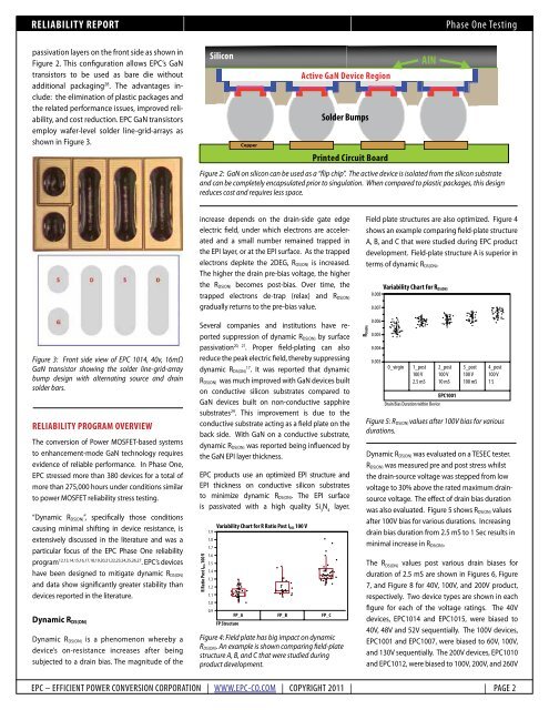
passivation layers on the front side as shown in<br />
Figure 2. This configuration allows <strong>EPC</strong>’s <strong>GaN</strong><br />
transistors to be used as bare die without<br />
additional packaging 28 . The advantages include:<br />
the elimination of plastic packages and<br />
the related performance issues, improved reliability,<br />
and cost reduction. <strong>EPC</strong> <strong>GaN</strong> transistors<br />
employ wafer-level solder line-grid-arrays as<br />
shown in Figure 3.<br />
Silicon<br />
Copper<br />
Active <strong>GaN</strong> Device Region<br />
Solder Bumps<br />
Printed Circuit Board<br />
Figure 2: <strong>GaN</strong> on silicon can be used as a “flip chip”. The active device is isolated from the silicon substrate<br />
and can be completely encapsulated prior to singulation. When compared to plastic packages, this design<br />
reduces cost and requires less space.<br />
AlN<br />
Figure 3: Front side view of <strong>EPC</strong> 1014, 40v, 16mΩ<br />
<strong>GaN</strong> transistor showing the solder line-grid-array<br />
bump design with alternating source and drain<br />
solder bars.<br />
RELIABILITY PROGRAM OVERVIEW<br />
The conversion of Power MOSFET-based systems<br />
to enhancement-mode <strong>GaN</strong> technology requires<br />
evidence of reliable performance. In <strong>Phase</strong> <strong>One</strong>,<br />
<strong>EPC</strong> stressed more than 380 devices for a total of<br />
more than 275,000 hours under conditions similar<br />
to power MOSFET reliability stress testing.<br />
“Dynamic R DS(ON)”, specifically those conditions<br />
causing minimal shifting in device resistance, is<br />
extensively discussed in the literature and was a<br />
particular focus of the <strong>EPC</strong> <strong>Phase</strong> <strong>One</strong> reliability<br />
program 12,13,14,15,16,17,18,19,20,21,22,23,24,25,26,27 . <strong>EPC</strong>’s devices<br />
have been designed to mitigate dynamic R DS(ON)<br />
and data show significantly greater stability than<br />
devices reported in the literature.<br />
Dynamic R DS(ON)<br />
Dynamic R DS(ON) is a phenomenon whereby a<br />
device’s on-resistance increases after being<br />
subjected to a drain bias. The magnitude of the<br />
increase depends on the drain-side gate edge<br />
electric field, under which electrons are accelerated<br />
and a small number remained trapped in<br />
the EPI layer, or at the EPI surface. As the trapped<br />
electrons deplete the 2DEG, R DS(ON) is increased.<br />
The higher the drain pre-bias voltage, the higher<br />
the R DS(ON) becomes post-bias. Over time, the<br />
trapped electrons de-trap (relax) and R DS(ON)<br />
gradually returns to the pre-bias value.<br />
Several companies and institutions have reported<br />
suppression of dynamic R DS(ON) by surface<br />
passivation 20, 21 . Proper field-plating can also<br />
reduce the peak electric field, thereby suppressing<br />
dynamic R DS(ON)<br />
17<br />
. It was reported that dynamic<br />
R DS(ON) was much improved with <strong>GaN</strong> devices built<br />
on conductive silicon substrates compared to<br />
<strong>GaN</strong> devices built on non-conductive sapphire<br />
substrates 29 . This improvement is due to the<br />
conductive substrate acting as a field plate on the<br />
back side. With <strong>GaN</strong> on a conductive substrate,<br />
dynamic R DS(ON) was reported being influenced by<br />
the <strong>GaN</strong> EPI layer thickness.<br />
<strong>EPC</strong> products use an optimized EPI structure and<br />
EPI thickness on conductive silicon substrates<br />
to minimize dynamic R DS(ON). The EPI surface<br />
is passivated with a high quality Si 3<br />
N 4<br />
layer.<br />
R Ratio Post IDSS 100 V<br />
Variability Chart for R Ratio Post I DSS 100 V<br />
1.9<br />
1.8<br />
1.7<br />
1.6<br />
1.5<br />
1.4<br />
1.3<br />
1.2<br />
1.1<br />
1.0<br />
0.9<br />
FP_A FP_B FP_C<br />
FP Structure<br />
Figure 4: Field plate has big impact on dynamic<br />
R DS(ON). An example is shown comparing field-plate<br />
structure A, B, and C that were studied during<br />
product development.<br />
Field plate structures are also optimized. Figure 4<br />
shows an example comparing field-plate structure<br />
A, B, and C that were studied during <strong>EPC</strong> product<br />
development. Field-plate structure A is superior in<br />
terms of dynamic R DS(ON).<br />
RDS(ON)<br />
0.008<br />
0.007<br />
0.006<br />
0.005<br />
0.004<br />
0.003<br />
Variability Chart for R DS(ON)<br />
0_virgin<br />
1_post<br />
100 V<br />
2.5 mS<br />
2_post<br />
100 V<br />
10 mS<br />
<strong>EPC</strong>1001<br />
Drain Bias Duration within Device<br />
3_post<br />
100 V<br />
100 mS<br />
4_post<br />
100 V<br />
1 S<br />
Figure 5: R DS(ON) values after 100V bias for various<br />
durations.<br />
Dynamic R DS(ON) was evaluated on a TESEC tester.<br />
R DS(ON) was measured pre and post stress whilst<br />
the drain-source voltage was stepped from low<br />
voltage to 30% above the rated maximum drainsource<br />
voltage. The effect of drain bias duration<br />
was also evaluated. Figure 5 shows R DS(ON) values<br />
after 100V bias for various durations. Increasing<br />
drain bias duration from 2.5 mS to 1 Sec results in<br />
minimal increase in R DS(ON).<br />
The R DS(ON) values post various drain biases for<br />
duration of 2.5 mS are shown in Figures 6, Figure<br />
7, and Figure 8 for 40V, 100V, and 200V product,<br />
respectively. Two device types are shown in each<br />
figure for each of the voltage ratings. The 40V<br />
devices, <strong>EPC</strong>1014 and <strong>EPC</strong>1015, were biased to<br />
40V, 48V and 52V sequentially. The 100V devices,<br />
<strong>EPC</strong>1001 and <strong>EPC</strong>1007, were biased to 60V, 100V,<br />
and 130V sequentially. The 200V devices, <strong>EPC</strong>1010<br />
and <strong>EPC</strong>1012, were biased to 100V, 200V, and 260V<br />
<strong>EPC</strong> – EFFICIENT POWER CONVERSION CORPORATION | WWW.<strong>EPC</strong>-CO.COM | COPYRIGHT 2011 | | PAGE 2