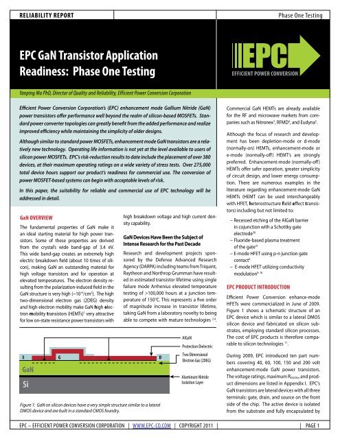
EPC GaN Transistor Application Readiness Phase One Testing Standard relatively
EPC GaN Transistor Application Readiness: Phase One Testing
EPC GaN Transistor Application Readiness: Phase One Testing
- No tags were found...

You also want an ePaper? Increase the reach of your titles
YUMPU automatically turns print PDFs into web optimized ePapers that Google loves.
RELIABILITY REPORT<br />
<strong>Phase</strong> <strong>One</strong> <strong>Testing</strong><br />
<strong>EPC</strong> <strong>GaN</strong> <strong>Transistor</strong> <strong>Application</strong><br />
<strong>Readiness</strong>: <strong>Phase</strong> <strong>One</strong> <strong>Testing</strong><br />
EFFICIENT POWER CONVERSION<br />
Yanping Ma PhD, Director of Quality and Reliability, Efficient Power Conversion Corporation<br />
Efficient Power Conversion Corporation’s (<strong>EPC</strong>) enhancement mode Gallium Nitride (<strong>GaN</strong>)<br />
power transistors offer performance well beyond the realm of silicon-based MOSFETs. <strong>Standard</strong><br />
power converter topologies can greatly benefit from the added performance and realize<br />
improved efficiency while maintaining the simplicity of older designs.<br />
Although similar to standard power MOSFETs, enhancement mode <strong>GaN</strong> transistors are a <strong>relatively</strong><br />
new technology. Operating life information is not yet at the level available to users of<br />
silicon power MOSFETs. <strong>EPC</strong>’s risk-reduction results to date include the placement of over 380<br />
devices, at their maximum operating ratings on a wide variety of stress tests. Over 275,000<br />
total device hours support our product’s readiness for commercial use. The conversion of<br />
power MOSFET-based systems can begin with acceptable levels of risk.<br />
In this paper, the suitability for reliable and commercial use of <strong>EPC</strong> technology will be<br />
addressed in detail.<br />
<strong>GaN</strong> OVERVIEW<br />
The fundamental properties of <strong>GaN</strong> make it<br />
an ideal starting material for high power transistors.<br />
Some of these properties are derived<br />
from the crystal’s wide band-gap of 3.4 eV.<br />
This wide band-gap creates an extremely high<br />
electric breakdown field (about 10 times of silicon),<br />
making <strong>GaN</strong> an outstanding material for<br />
high voltage transistors and for operation at<br />
elevated temperatures. The electron density resulting<br />
from the polarization-induced field in the<br />
<strong>GaN</strong> structure is very high (~10 13 /cm 2 ). The high<br />
two-dimensional electron gas (2DEG) density<br />
and high electron mobility make <strong>GaN</strong> high electron<br />
mobility transistors (HEMTs) 1 very attractive<br />
for low on-state resistance power transistors with<br />
S G D<br />
<strong>GaN</strong><br />
Si<br />
Figure 1: <strong>GaN</strong> on silicon devices have a very simple structure similar to a lateral<br />
DMOS device and are built in a standard CMOS foundry.<br />
high breakdown voltage and high current density<br />
capability.<br />
<strong>GaN</strong> Devices Have Been the Subject of<br />
Intense Research for the Past Decade<br />
Research and development projects sponsored<br />
by the Defense Advanced Research<br />
Agency (DARPA) including teams from Triquint,<br />
Raytheon and Northrop Grumman have resulted<br />
in estimated transistor lifetime using single<br />
failure mode Arrhenius elevated temperature<br />
testing of >100,000 hours at a junction temperature<br />
of 150°C. This represents a five order<br />
of magnitude increase in transistor lifetime,<br />
taking <strong>GaN</strong> from a laboratory novelty to being<br />
able to compete with mature technologies 2,4 .<br />
AI<strong>GaN</strong><br />
Protection Dielectric<br />
Two Dimensional<br />
Electron Gas (2DEG)<br />
Aluminum Nitride<br />
Isolation Layer<br />
Commercial <strong>GaN</strong> HEMTs are already available<br />
for the RF and microwave markets from companies<br />
such as Nitronex 3 , RFMD 4 , and Eudyna 5 .<br />
Although the focus of research and development<br />
has been depletion-mode or d-mode<br />
(normally-on) HEMTs, enhancement-mode or<br />
e-mode (normally-off) HEMT’s are strongly<br />
preferred. Enhancement-mode (normally-off)<br />
HEMTs offer safer operation, greater simplicity<br />
of circuit design, and lower energy consumption.<br />
There are numerous examples in the<br />
literature regarding enhancement-mode <strong>GaN</strong><br />
HEMTs (HEMT can be used interchangeably<br />
with HFET, heterostructure field effect transistors)<br />
including but not limited to:<br />
− Recessed etching of the Al<strong>GaN</strong> barrier<br />
in cojunction with a Schottky gate<br />
electrode 30<br />
− Fluoride-based plasma treatment<br />
of the gate 31<br />
− E-mode HFET using p-n junction gate<br />
contact 6<br />
− E-mode HFET utilizing conductivity<br />
9, 10<br />
modulation<br />
<strong>EPC</strong> PRODUCT INTRODUCTION<br />
Efficient Power Conversion enhance-mode<br />
HFETs were commercialized in June of 2009.<br />
Figure 1 shows a schematic structure of an<br />
<strong>EPC</strong> device which is similar to a lateral DMOS<br />
silicon device and fabricated on silicon substrates,<br />
employing standard silicon processes.<br />
The cost of <strong>EPC</strong> products is therefore comparable<br />
to silicon technologies 11 .<br />
During 2009, <strong>EPC</strong> introduced ten part numbers<br />
covering 40, 60, 100, 150 and 200 volt<br />
enhancement-mode <strong>GaN</strong> power transistors.<br />
The voltage ratings, maximum R DS(ON), and product<br />
dimensions are listed in Appendix I. <strong>EPC</strong>’s<br />
<strong>GaN</strong> transistors are lateral devices with all three<br />
terminals: gate, drain, and source on the front<br />
side of the chip. The active device is isolated<br />
from the substrate and fully encapsulated by<br />
<strong>EPC</strong> – EFFICIENT POWER CONVERSION CORPORATION | WWW.<strong>EPC</strong>-CO.COM | COPYRIGHT 2011 | | PAGE 1
RELIABILITY REPORT<br />
<strong>Phase</strong> <strong>One</strong> <strong>Testing</strong><br />
passivation layers on the front side as shown in<br />
Figure 2. This configuration allows <strong>EPC</strong>’s <strong>GaN</strong><br />
transistors to be used as bare die without<br />
additional packaging 28 . The advantages include:<br />
the elimination of plastic packages and<br />
the related performance issues, improved reliability,<br />
and cost reduction. <strong>EPC</strong> <strong>GaN</strong> transistors<br />
employ wafer-level solder line-grid-arrays as<br />
shown in Figure 3.<br />
Silicon<br />
Copper<br />
Active <strong>GaN</strong> Device Region<br />
Solder Bumps<br />
Printed Circuit Board<br />
Figure 2: <strong>GaN</strong> on silicon can be used as a “flip chip”. The active device is isolated from the silicon substrate<br />
and can be completely encapsulated prior to singulation. When compared to plastic packages, this design<br />
reduces cost and requires less space.<br />
AlN<br />
Figure 3: Front side view of <strong>EPC</strong> 1014, 40v, 16mΩ<br />
<strong>GaN</strong> transistor showing the solder line-grid-array<br />
bump design with alternating source and drain<br />
solder bars.<br />
RELIABILITY PROGRAM OVERVIEW<br />
The conversion of Power MOSFET-based systems<br />
to enhancement-mode <strong>GaN</strong> technology requires<br />
evidence of reliable performance. In <strong>Phase</strong> <strong>One</strong>,<br />
<strong>EPC</strong> stressed more than 380 devices for a total of<br />
more than 275,000 hours under conditions similar<br />
to power MOSFET reliability stress testing.<br />
“Dynamic R DS(ON)”, specifically those conditions<br />
causing minimal shifting in device resistance, is<br />
extensively discussed in the literature and was a<br />
particular focus of the <strong>EPC</strong> <strong>Phase</strong> <strong>One</strong> reliability<br />
program 12,13,14,15,16,17,18,19,20,21,22,23,24,25,26,27 . <strong>EPC</strong>’s devices<br />
have been designed to mitigate dynamic R DS(ON)<br />
and data show significantly greater stability than<br />
devices reported in the literature.<br />
Dynamic R DS(ON)<br />
Dynamic R DS(ON) is a phenomenon whereby a<br />
device’s on-resistance increases after being<br />
subjected to a drain bias. The magnitude of the<br />
increase depends on the drain-side gate edge<br />
electric field, under which electrons are accelerated<br />
and a small number remained trapped in<br />
the EPI layer, or at the EPI surface. As the trapped<br />
electrons deplete the 2DEG, R DS(ON) is increased.<br />
The higher the drain pre-bias voltage, the higher<br />
the R DS(ON) becomes post-bias. Over time, the<br />
trapped electrons de-trap (relax) and R DS(ON)<br />
gradually returns to the pre-bias value.<br />
Several companies and institutions have reported<br />
suppression of dynamic R DS(ON) by surface<br />
passivation 20, 21 . Proper field-plating can also<br />
reduce the peak electric field, thereby suppressing<br />
dynamic R DS(ON)<br />
17<br />
. It was reported that dynamic<br />
R DS(ON) was much improved with <strong>GaN</strong> devices built<br />
on conductive silicon substrates compared to<br />
<strong>GaN</strong> devices built on non-conductive sapphire<br />
substrates 29 . This improvement is due to the<br />
conductive substrate acting as a field plate on the<br />
back side. With <strong>GaN</strong> on a conductive substrate,<br />
dynamic R DS(ON) was reported being influenced by<br />
the <strong>GaN</strong> EPI layer thickness.<br />
<strong>EPC</strong> products use an optimized EPI structure and<br />
EPI thickness on conductive silicon substrates<br />
to minimize dynamic R DS(ON). The EPI surface<br />
is passivated with a high quality Si 3<br />
N 4<br />
layer.<br />
R Ratio Post IDSS 100 V<br />
Variability Chart for R Ratio Post I DSS 100 V<br />
1.9<br />
1.8<br />
1.7<br />
1.6<br />
1.5<br />
1.4<br />
1.3<br />
1.2<br />
1.1<br />
1.0<br />
0.9<br />
FP_A FP_B FP_C<br />
FP Structure<br />
Figure 4: Field plate has big impact on dynamic<br />
R DS(ON). An example is shown comparing field-plate<br />
structure A, B, and C that were studied during<br />
product development.<br />
Field plate structures are also optimized. Figure 4<br />
shows an example comparing field-plate structure<br />
A, B, and C that were studied during <strong>EPC</strong> product<br />
development. Field-plate structure A is superior in<br />
terms of dynamic R DS(ON).<br />
RDS(ON)<br />
0.008<br />
0.007<br />
0.006<br />
0.005<br />
0.004<br />
0.003<br />
Variability Chart for R DS(ON)<br />
0_virgin<br />
1_post<br />
100 V<br />
2.5 mS<br />
2_post<br />
100 V<br />
10 mS<br />
<strong>EPC</strong>1001<br />
Drain Bias Duration within Device<br />
3_post<br />
100 V<br />
100 mS<br />
4_post<br />
100 V<br />
1 S<br />
Figure 5: R DS(ON) values after 100V bias for various<br />
durations.<br />
Dynamic R DS(ON) was evaluated on a TESEC tester.<br />
R DS(ON) was measured pre and post stress whilst<br />
the drain-source voltage was stepped from low<br />
voltage to 30% above the rated maximum drainsource<br />
voltage. The effect of drain bias duration<br />
was also evaluated. Figure 5 shows R DS(ON) values<br />
after 100V bias for various durations. Increasing<br />
drain bias duration from 2.5 mS to 1 Sec results in<br />
minimal increase in R DS(ON).<br />
The R DS(ON) values post various drain biases for<br />
duration of 2.5 mS are shown in Figures 6, Figure<br />
7, and Figure 8 for 40V, 100V, and 200V product,<br />
respectively. Two device types are shown in each<br />
figure for each of the voltage ratings. The 40V<br />
devices, <strong>EPC</strong>1014 and <strong>EPC</strong>1015, were biased to<br />
40V, 48V and 52V sequentially. The 100V devices,<br />
<strong>EPC</strong>1001 and <strong>EPC</strong>1007, were biased to 60V, 100V,<br />
and 130V sequentially. The 200V devices, <strong>EPC</strong>1010<br />
and <strong>EPC</strong>1012, were biased to 100V, 200V, and 260V<br />
<strong>EPC</strong> – EFFICIENT POWER CONVERSION CORPORATION | WWW.<strong>EPC</strong>-CO.COM | COPYRIGHT 2011 | | PAGE 2
RELIABILITY REPORT<br />
<strong>Phase</strong> <strong>One</strong> <strong>Testing</strong><br />
RDS(ON)<br />
0.020<br />
0.015<br />
0.010<br />
0.005<br />
0.000<br />
0_virgin<br />
1_post 40 V<br />
2_post 48 V<br />
3_post 52 V<br />
0_virgin<br />
<strong>EPC</strong>1014<br />
Drain Source Bias within Device<br />
1_post 40 V<br />
2_post 48 V<br />
<strong>EPC</strong>1015<br />
3_post 52 V<br />
RDS(ON)<br />
0.040<br />
0.035<br />
0.030<br />
0.025<br />
0.020<br />
0.015<br />
0.010<br />
0.005<br />
0.000<br />
0_virgin<br />
1_post 60 V<br />
2_post 100 V<br />
3_post 130 V<br />
<strong>EPC</strong>1001<br />
Drain Source Bias within Device<br />
0_virgin<br />
1_post 60 V<br />
2_post 100 V<br />
<strong>EPC</strong>1007<br />
3_post 130 V<br />
RDS(ON)<br />
0.10<br />
0.09<br />
0.08<br />
0.07<br />
0.06<br />
0.05<br />
0.04<br />
0.03<br />
0.02<br />
0.01<br />
0.00<br />
0_virgin<br />
1_post 100 V<br />
2_post 200 V<br />
3_post 260 V<br />
0_virgin<br />
<strong>EPC</strong>1010<br />
Drain Source Bias within Device<br />
1_post 100 V<br />
2_post 200 V<br />
3_post 260 V<br />
<strong>EPC</strong>1012<br />
Figure 6: The R DS(ON) values post various drain<br />
biases are shown for <strong>EPC</strong>1014 and <strong>EPC</strong>1015,<br />
the two 40V products.<br />
Figure 7: The R DS(ON) values post various drain<br />
biases are shown for <strong>EPC</strong>1001 and <strong>EPC</strong>1007,<br />
the two 100V products.<br />
Figure 8: The R DS(ON) values post various drain<br />
biases are shown for <strong>EPC</strong>1010 and <strong>EPC</strong>1012,<br />
the two 200V products.<br />
sequentially. The degree of dynamic R DS(ON) was<br />
similar for all product types. The increase in R DS(ON)<br />
for the main population was approximately 10%<br />
with a tail at higher or lower values.<br />
RELIABILITY TESTING OVERVIEW<br />
AND RESULTS<br />
Long term stability under high drain-source<br />
bias was evaluated by subjecting devices<br />
to DC voltage equal to the maximum drainsource<br />
rated voltage and temperature (high<br />
temperature reverse bias, or HTRB). Gate<br />
reliability was evaluated by subjecting devices<br />
to various gate stresses at elevated temperature<br />
(high temperature gate bias, or HTGB).<br />
Environmental reliability was evaluated with<br />
temperature cycling (TC) and temperaturehumidity-with-bias<br />
(THB). Devices were also<br />
subjected to operating life tests involving<br />
devices in actual power supplies running at<br />
high voltage and high current.<br />
A list of the reliability tests performed, the applicable<br />
standards, the device types evaluated,<br />
and the stress conditions are listed in Appendix<br />
II. All devices tested were soldered onto Arlon<br />
85N printed circuit boards.<br />
HighTemperature<br />
Reverse Bias Test (HTRB)<br />
The impact of high drain bias on device parameters,<br />
applied for long periods of time, was evaluated<br />
with maximum rated drain-source bias<br />
applied at an ambient temperature of 125ºC.<br />
Whereas there were no parametric failures out<br />
of the parts tested, there was some degree of<br />
dynamic R DSON post stress test (A 20% increase in<br />
R DSON was observed for some devices).<br />
All electric parameters remained <strong>relatively</strong><br />
constant throughout the entire stress<br />
period of 1000 hours for <strong>EPC</strong>1001 and <strong>EPC</strong>1014.<br />
Appendix IV graphically presents the stability<br />
of various device parameters during test.<br />
High Temperature Gate Bias Test (HTGB)<br />
The gate stability of <strong>EPC</strong> <strong>GaN</strong> transistors was<br />
evaluated under various gate bias conditions<br />
at 5V, 5.4V, and 6V at 125ºC. <strong>EPC</strong>1001 parts<br />
were used for each of the three tests. At 5Vgs<br />
and 5.4Vgs bias, all device electric parameters<br />
stayed <strong>relatively</strong> constant over the entire<br />
burn-in period of 1000 hours. It was observed<br />
though that the drain leakage increased with<br />
6Vgs bias. Five parts showed higher than the<br />
datasheet limit at the 168 hours pulling point<br />
(Appendix III *). These parts were put back on<br />
burn-in, and will be analyzed after the stress<br />
test is finished. Complete test results are presented<br />
in Appendix V.<br />
Temp Cycle (TC)<br />
Temperature cycling was conducted on<br />
<strong>EPC</strong>1001, a large device, and on <strong>EPC</strong>1014, a<br />
small device. These two part numbers have different<br />
bump designs and were used to check<br />
the bump joint reliability. Parts were all mounted<br />
on Arlon 85N printed circuit board material.<br />
Temperatures varied between -40C to 125ºC at<br />
a rate of two cycles per hour. No on-state resistance<br />
degradation was observed over the stress<br />
period of 1000 cycles. All electrical parameters<br />
remained constant during stress. Complete test<br />
results are shown in Appendix VI.<br />
Temperature Humidity Bias Test (THB)<br />
Device performance was also characterized with<br />
temperature and humidity with drain-source<br />
bias (THB). THB tests were conducted at 85ºC<br />
and with 85% relative humidity. <strong>EPC</strong>1014 was<br />
on test with drain biased to the rated 40 volt.<br />
At time of this writing, parts have completed<br />
500 hours stress, and are continuing on test<br />
for 1000 hours. All device electric parameters<br />
remained <strong>relatively</strong> constant over the stress<br />
period. Complete test results are shown in<br />
Appendix VII.<br />
Power Supply Operating Life Test<br />
To demonstrate the performance of the <strong>GaN</strong><br />
transistors in-circuit, and to test the reliability<br />
under high-stress operating life, <strong>EPC</strong> built<br />
48V-1V power supply boards using a “buck converter”<br />
topology (see figure 9). For the burn-in<br />
test, <strong>EPC</strong>1001 (100V, 7 mΩ) transistors were used<br />
for both the control transistor and rectifier switches.<br />
This kind of test is particularly useful because,<br />
in a standard “buck” topology DC-DC converter<br />
operated at the high Vin/Vout ratio of 48V:1V, the<br />
control transistor is turned ON at a very low duty<br />
cycle (~2%). Conversely, the rectifier transistor is<br />
turned ON with a very high duty cycle (~98%). This<br />
test therefore stresses devices both at high drainsource<br />
voltage and high drain current under actual,<br />
fast-switching conditions. The converter was<br />
operated at 48V input voltage, 1V output voltage,<br />
10A output current, and at a switching frequency<br />
of 250 kHz. The circuit efficiency was measured<br />
at time-zero hour, 24, 48, 72, 168, 500, 1000, and<br />
1200 hours. The normalized efficiency vs. burnin<br />
hours is plotted in Figure 9(a), and the power<br />
supply test circuit is shown in Figure 9(b). The<br />
efficiency of all the power supply boards stayed<br />
virtually unchanged over the entire burn-in<br />
period.<br />
<strong>EPC</strong> – EFFICIENT POWER CONVERSION CORPORATION | WWW.<strong>EPC</strong>-CO.COM | COPYRIGHT 2011 | | PAGE 3
RELIABILITY REPORT<br />
FUTURE WORK<br />
<strong>EPC</strong> has plans for a much broader and deeper<br />
study of the reliability of enhancement mode<br />
<strong>GaN</strong> power transistors. In <strong>Phase</strong> 2, <strong>EPC</strong> will complete<br />
the 1000 hour/1000 cycle testing on all<br />
product types. Further work will also be done<br />
to develop acceleration factors and models that<br />
allow users to determine suitability for various<br />
applications beyond basic commercial use.<br />
Dynamic R DS(ON) will continue to be investigated<br />
with the goal of further minimizing this characteristic<br />
of <strong>EPC</strong> <strong>GaN</strong> devices.<br />
<strong>EPC</strong> will convert to lead free solder in the second<br />
half of 2010. This conversion will be accompanied<br />
by additional testing at 150ºC to verify this<br />
change does not degrade device characteristics<br />
under stress. At that time, <strong>EPC</strong> will also conduct<br />
temperature cycling tests on a wide variety of<br />
substrate materials to validate compatibility.<br />
SUMMARY<br />
y<br />
<strong>Phase</strong> <strong>One</strong> <strong>Testing</strong><br />
1.30<br />
1.20<br />
1.10<br />
1.00<br />
0.90<br />
0.80<br />
0.70<br />
1 10 100 1000 10000<br />
Burn-In Hours<br />
<strong>EPC</strong>’s enhancement mode Gallium Nitride transistors<br />
bring tremendous performance and size<br />
advantages over silicon power MOSFETs. These<br />
advantages can be used to improve system efficiency,<br />
reduce system cost, reduce size, or a<br />
combination of all three. Because <strong>EPC</strong>’s products<br />
were designed as power MOSFET replacements,<br />
designers can use their existing building<br />
blocks, skills and knowledge with only minor<br />
changes. Reliability testing has also demonstrated<br />
that the technology is now ready for<br />
general commercial use.<br />
The future of <strong>GaN</strong> transistors is now.<br />
Figure 9(a): Power supply life test using <strong>EPC</strong>1001 at 30oC and 10A. The normalized converter efficiency was<br />
plotted over 1200 hours of operating life.<br />
V IN<br />
+<br />
-<br />
Q CONTROL<br />
Figure 9(b): Power supply test circuit<br />
L<br />
Q RECTIFIER<br />
+<br />
-<br />
I OUT<br />
V OUT<br />
Load<br />
<strong>EPC</strong> – EFFICIENT POWER CONVERSION CORPORATION | WWW.<strong>EPC</strong>-CO.COM | COPYRIGHT 2011 | | PAGE 4
RELIABILITY REPORT<br />
<strong>Phase</strong> <strong>One</strong> <strong>Testing</strong><br />
References<br />
REFERENCES<br />
1. M. Asif Khan, A. Bhattarai, J.N. Kuznia, and D.T. Olson, “High Electron Mobility <strong>Transistor</strong> Based on a <strong>GaN</strong>-AlxGa1-xN Heterojunction,” Appl. Phys. Lett., vol. 63, no. 9, 1993, pp. 1214-1215.<br />
2. M.J. Rosker, “The Present State of the Art of Wide-Bandgap Semiconductors and Their Future,” in Proc. IEEE Radio Freq. Integr. Circuit Symp., 2007, pp. 159-162.<br />
3. http://www.nitronex.com<br />
4. http://ir.rfmd.com/releasedetail.cfm?ReleaseID=412122<br />
5. http://www.mwrf.com/Article/ArticleID/13434/13434.html<br />
6. X. Hu, J. Simin, J. Yang, M. Asif Khan, R. Gaska, and M.S. Shur, “Enhancement Mode Al<strong>GaN</strong>/<strong>GaN</strong> HFET with Selectively Grown PN Junction Gate,” Electronics Letters, 2000, vol. 36, no. 8, pp. 753-754.<br />
7. N. Tsuyuchi, K. Nagamatsu, Y. Hirose, M, Iwaya, S. Kamiyama, H. Amano, and I. Akasaki, “Low-Leakage-Current Enhancement-Mode Al<strong>GaN</strong>/<strong>GaN</strong> Heterostructure Field-Effect <strong>Transistor</strong> Using p-Type Gate Contact,” Jpn. J. Appl. Phys.,<br />
vol. 45, 2006, pp. L319-L321.<br />
8. T. Fujii, N. Tsuyukuchi, M. Iwaya, S. Kamiyama, H. Amano, and I. Akasaki, “High on/off Ratio in Enhancement –Mode AlxGa1-xN/<strong>GaN</strong> Junction Heterostructure Field-Effect <strong>Transistor</strong>s with p-Type <strong>GaN</strong> Gate Contact,” Jpn J. Appl.<br />
Phys., vol. 45, no. 39, 2006, pp. L1048-L1050.<br />
9. Y. Uemoto, M. Hikita, H. Ueno, H. Matsuo, H. Ishida, M. Yanagihar, T. Ueda, T. Tanaka, and D. Ueda, “Gate Injection <strong>Transistor</strong> (GIT) – A Normally-off Al<strong>GaN</strong>/<strong>GaN</strong> Power <strong>Transistor</strong> Using Conductivity Modulation,” IEEE Transactions on<br />
Electron Devices, vol. 54, no. 12, 2007, pp. 3393-3399.<br />
10. Y. Uemoto, T. Ueda, T. Tanaka, D. Ueda, “Recent Advances of High Voltage Al<strong>GaN</strong>/<strong>GaN</strong> Power HFETs,” in Proc. of SPIE Vol. 7216, 721606, 2009, pp.1-11.<br />
11. A. Lidow, “Is it the End of the Road for Silicon in Power Conversion?” CIPS 2010 Conference Proceedings, March 2010, Nurnberg, Germany.<br />
12. W. Saito, M. Kuraguchi, Y. Takada, K. Tsuda, T. Domon, I. Omura, and M. Yamaguchi, “380 V/1.9A <strong>GaN</strong> power-HEMT: Current collapse phenomena under high applied voltage and demonstration of 27.1 MHz class-E amplifier,” in<br />
IEDM Tech. Dig., 2005, pp. 597-600.<br />
13. S. Singhal, J.C. Roberts, P. Rajagopal, T. Li, A.W. Hanson, R. Therrien, J.W. Johnson, I.C. Kizilyalli, K.J. Linthicum, “<strong>GaN</strong>-on-Si failure mechanisms and reliability improvements,” in Proc. IEEE Int. Rel. Phys. Symp., 2006, pp. 95-98.<br />
14. S. Singhal, T. Li, A. ,Chaudhari, A.W. Hanson, R. Theerien, J.W. Johnson, W. Nagy, J. Marquart, P. Rajagopal, J.C. Roberts, E.L. Piner, I.C. Kizilyalli, K.J. Linthicum, “Reliability of Large Periphery <strong>GaN</strong>-on-Si HFETs,” Microelectronics Reliability<br />
46, 2006, pp. 1247-1253.<br />
15. P. Saunier, C. Lee, A. Galistreri, D. Dumka, J. Jimenez, H.Q. Tserng, M.Y. Kao, P.C. Chao, K. Chu, A. Souzis, I. Eliashevich, S. Guo, J. del Alama, J. Joh, M. Shur, “Progress in <strong>GaN</strong> Performances and Reliability,” in Proc. Device Res. Conf., 2007,<br />
pp. 35-36.<br />
16. G. Meneghesso, G. Verellesi, F. Danesin, F. Rampazzo, F. Zanon, A. Tazzoli, M. Meneghini, and E. Zanoni, “Reliability of <strong>GaN</strong> high-electron-mobility transistors: state of the art and perspectives,” IEEE Transactions on Device and<br />
Materials Reliability, vol. 8, no. 2, 2008, pp. 332-343.<br />
17. W. Saito, T. Nitta, Y. Kakiuchi, Y. Saito, K. Tsuda, I. Omura, and M. Yamaguchi, “On-Resistance Modulation of High Voltage <strong>GaN</strong> HEMT on Sapphire Substrate Under High Applied Voltage,” IEEE Electron Device Letters, vol. 28, no. 8,<br />
2007, pp. 676-678.<br />
18. D. Marcon, A. Lorenz, J. Derluyn, J. Das, F. Medjdoub, K. Cheng, S. Degroote, M. Leys, R. Mertens, M. Germain, and G. Borghs, “<strong>GaN</strong>-on-Si HEMT stress under high electric field condition,” Phys. Status Solidi C, vol. 6, 2009, pp. S1024-<br />
S1028.<br />
19. R. Vetury, N.Q. Zhang, S. Keller, U.K. Mishra, “The impact of surface states on the DC and RF characteristics of Al<strong>GaN</strong>/<strong>GaN</strong> HFETs,” IEEE Transactions on Electron Devices, vol. 48, no. 3, 2001, pp. 560-566.<br />
20. L. Ma, Y. Wang, T.Y. Guo, J. Lu, Z.B. Hao, Y. Luo, and Z.P. Yu, “Trap Related Current Collapse Effects in <strong>GaN</strong> HEMTs,” IEEE Conf. on Electron Devices and Solid State Circuits, 2005, pp. 795-798.<br />
21. T. Mizutani, Y. Ohno, M. Akita, S. Kishimoto, and K. Maezawa, “A Study on Current Collapse in Al<strong>GaN</strong>/<strong>GaN</strong> HEMTs Inducted by Bias Stress,” IEEE Transactions on Electron Devices, Vol. 50, No. 10, 2003, pp. 2015-2020.<br />
22. L. Shen, S. Heikman, B. Moran, et al., “Al<strong>GaN</strong>/AlN/<strong>GaN</strong> High-Power Microwave HEMT,” IEEE Electron Device Letters., vol. 22, 2001, pp.457-459.<br />
23. Y.C. Chou, D. Leung, I Smorchkova, M, Wojtowicz, R. Grundbacher, L. Callejo, Q. Kan, R. Lai, P.H. Liu, D. Eng, A. Oki, “Degradation of Al<strong>GaN</strong>/<strong>GaN</strong> HEMTs Under Elevated Temperature Life testing,” Microelectronics Reliability, vol. 44,<br />
2004, pp. 1033-1038.<br />
24. N. Shgaier, M. Trabelsi, N. Yacoubi, J.M. Bluet, A. Souifi, G. Guillot, C. Gaquiere, J.C. DeJaeger, “Traps Centers and Deep Defects Contribution in Current Instabilities for Al<strong>GaN</strong>/<strong>GaN</strong> HEMT’s on Silicon and Sapphire Substrates,” Microelectronics<br />
Journal 37, 2006, pp. 363-370.<br />
25. J. Joh, and J. del Alamo, “Mechanism for Electrical Degradation of <strong>GaN</strong> High-Electron Mobility <strong>Transistor</strong>s,” in IEDM Tch. Dig., 2006, pp. 415-418.<br />
26. S.Y. Park, C. Floresca, U. Chowdhury, J.L. Jimenez, C. Lee, E. Beam, P. Saunier, T. Balistreri, M.J. Kim, “Physical Degradation of <strong>GaN</strong> HEMT Devices Under Drain Bias Reliability <strong>Testing</strong>,” Microelectronics Reliability, vol. 49, 2009, pp. 478-<br />
483.<br />
27. D. Kumar Sahoo, R.K. Lal, H. Kim, V. Tilak, and L.F. Eastman, “High-field effects in silicon nitride passivated <strong>GaN</strong> MODEFTs,” IEEE Transactions on Electron Devices, vol. 50, no. 5, 2003, pp. 1163-1170.<br />
28. A.M. Conway, M. Chen, P. Hashimoto, P.J. Willadsen, and M. Micovic, “Failure Mechanisms in <strong>GaN</strong> HFETs under Accelerated RF Stress,” CS MANTECH Conference, May 14-17, 2007, Austin Texas.<br />
29. N. Ikeda, S. Kaya, J. Li, Y. Sato, S. Kato, S. Yoshida, “High power Al<strong>GaN</strong>/<strong>GaN</strong> HFET with a high breakdown voltage of over 1.8KV on 4 inch Si substrate and suppression of current collapse,” Proceedings of the 20th International<br />
Symposium on Power Semiconductor Devices and IC’s, 2008, pp. 287-290.<br />
30. V. Kumar, A. Kuliev, T. Tanaka, Y. Otoki, I. Adesida, “High transconductance enhancement-mode Al<strong>GaN</strong>/<strong>GaN</strong> HEMTs on SiC substrate,” Electronics Letters, vol. 39, no. 24, 2003, pp. 1758-1760.<br />
31. Y. Cai, Y. Zhou, K. J. Chen, K. M. Lau, “High Performance Enhancement-Mode Al<strong>GaN</strong>/<strong>GaN</strong> HEMT Using Fluoride-Based Plasma Treatment,” IEEE Electron Device Letters, vol. 26, no. 7, 2005, pp. 435-437.<br />
<strong>EPC</strong> – EFFICIENT POWER CONVERSION CORPORATION | WWW.<strong>EPC</strong>-CO.COM | COPYRIGHT 2011 | | PAGE 5
RELIABILITY REPORT<br />
<strong>Phase</strong> <strong>One</strong> <strong>Testing</strong><br />
Appendix<br />
APPENDIX I: . . . . . . . . . . . . . . . . . . . . . . . . . Product Matrix Table<br />
APPENDIX II: . . . . . . . . . . . . . . . . . . . . . . . . . . Reliability Test Table<br />
APPENDIX III: . . . . . . . . . . . . . . . . . . . . . . . Reliability Results Table<br />
APPENDIX IV: . . . . . . . . . . . . . . . . . . . . . . . . . . . . . HTRB Results<br />
APPENDIX V: . . . . . . . . . . . . . . . . . . . . . . . . . . . . . .HTGB Results<br />
APPENDIX VI: . . . . . . . . . . . . . . . . . . . . . . . . . . . . . . . .TC Results<br />
APPENDIX VII: . . . . . . . . . . . . . . . . . . . . . . . . . . . . . . THB Results<br />
APPENDIX VIII: . . . . . . . . . . . . . Power Supply Operating Life Results<br />
<strong>EPC</strong> – EFFICIENT POWER CONVERSION CORPORATION | WWW.<strong>EPC</strong>-CO.COM | COPYRIGHT 2011 | | PAGE 6
RELIABILITY REPORT<br />
<strong>Phase</strong> <strong>One</strong> <strong>Testing</strong><br />
Appendix I: Product Matrix Table<br />
Voltage Rating R DS(ON) Max Package Dimensions<br />
Part Number<br />
(V) (mOhm) (mm x mm)<br />
<strong>EPC</strong>1014 40 16 LGA 1.7 X 1.1<br />
<strong>EPC</strong>1015 40 4 LGA 4.1 X 1.6<br />
<strong>EPC</strong>1009 60 30 LGA 1.7 X 1.1<br />
<strong>EPC</strong>1005 60 7 LGA 4.1 X 1.6<br />
<strong>EPC</strong>1007 100 30 LGA 1.7 X 1.1<br />
<strong>EPC</strong>1001 100 7 LGA 4.1 X 1.6<br />
<strong>EPC</strong>1013 150 100 LGA 1.7 X 0.9<br />
<strong>EPC</strong>1011 150 25 LGA 3.6 X 1.6<br />
<strong>EPC</strong>1012 200 100 LGA 1.7 X 0.9<br />
<strong>EPC</strong>1010 200 25 LGA 3.6 X 1.6<br />
Appendix II: Reliability Test Table<br />
Reliability Stress Test Applicable <strong>Standard</strong> Product Stress Conditions<br />
High Temperature Reverse Bias (HTRB) JEDEC Std JESD22-A108 <strong>EPC</strong>1001, <strong>EPC</strong>1014 100% rated drain bias, 125˚C<br />
High Temperature Gate Bias (HTGB) JEDEC Std JESD22-A108 <strong>EPC</strong>1001 5 V, 5.4 V, 6 V gate bias, 125˚C<br />
Temperature Cycling (TC) JEDEC Std JESD22-A104 <strong>EPC</strong>1001, <strong>EPC</strong>1014 -40˚C to 125˚C, 2 cycles per hour<br />
Temperature Humidity Bias (THB) JEDEC Std JESD22-A101 <strong>EPC</strong>1014 85˚C/85RH, rated drain bias or max 100 V drain bias<br />
Power Supply Operating Life <strong>EPC</strong>1001 10A, 250 kHz, 30˚C<br />
Appendix III: Reliability Results Table<br />
Stress Test Part Number Sample Size<br />
# of Fail at Read Point.1<br />
24HR 168HR 500HR Duration 1000HR<br />
HTRB <strong>EPC</strong>1001 45 0 0 0 0<br />
HTRB <strong>EPC</strong>1014 50 0 0 0 0<br />
Stress Test Part Number Sample Size<br />
# of Fail at Read Point.1<br />
24HR 168HR 500HR 1000HR<br />
HTGB 5 V <strong>EPC</strong>1001 45 0 0 0 0<br />
HTGB 5.4 V <strong>EPC</strong>1001 45 0 0 0 0<br />
HTGB 6 V <strong>EPC</strong>1001 50 0 5*<br />
Stress Test Part Number Sample Size<br />
# of Fail at Read Point.1<br />
48 cys 168 cys 500 cys 1000 cys<br />
TC <strong>EPC</strong>1001 45 0 0 0 0<br />
TC <strong>EPC</strong>1014 50 0 0 0 0<br />
Stress Test Part Number Sample Size<br />
# of Fail at Read Point.1<br />
24HR 168HR 500HR 1000HR<br />
THB <strong>EPC</strong>1014 45 0 0 0<br />
Stress Test Part Number Sample Size<br />
# of Fail at Read Point.1<br />
24HR 168HR 500HR 1000HR<br />
Power Supply Life Test <strong>EPC</strong>1001 10 0 0 0 0<br />
<strong>EPC</strong> – EFFICIENT POWER CONVERSION CORPORATION | WWW.<strong>EPC</strong>-CO.COM | COPYRIGHT 2011 | | PAGE 7
RELIABILITY REPORT<br />
<strong>Phase</strong> <strong>One</strong> <strong>Testing</strong><br />
Appendix IV: HTRB Maximum Rated Voltage at 125˚C<br />
<strong>EPC</strong>1001 HTRB 100 V at 125˚C<br />
Normalized RDS(ON)<br />
HTRB <strong>EPC</strong>1001 R DS(ON) vs. Stress Time<br />
2.0<br />
1.8<br />
1.6<br />
1.4<br />
1.2<br />
1.0<br />
0.8<br />
0.6<br />
0.4<br />
0.2<br />
0.0<br />
1 10 100 1000<br />
Stress Hours<br />
IGSS @ 5 V (µA)<br />
HTRB <strong>EPC</strong>1001 I GSS @ 5 V vs. Stress Time<br />
5000<br />
4500<br />
4000<br />
3500<br />
3000<br />
2500<br />
2000<br />
1500<br />
1000<br />
500<br />
0<br />
1 10 100 1000<br />
Stress Hours<br />
Normalized VTH<br />
HTRB <strong>EPC</strong>1001 V TH vs. Stress Time<br />
2.0<br />
1.8<br />
1.6<br />
1.4<br />
1.2<br />
1.0<br />
0.8<br />
0.6<br />
0.4<br />
0.2<br />
0.0<br />
1 10 100 1000<br />
Stress Hours<br />
IDSS @ 100 V (µA)<br />
HTRB <strong>EPC</strong>1001 I DSS vs. Stress Time<br />
300<br />
250<br />
200<br />
150<br />
100<br />
50<br />
0 1 10 100 1000<br />
Stress Hours<br />
<strong>EPC</strong> – EFFICIENT POWER CONVERSION CORPORATION | WWW.<strong>EPC</strong>-CO.COM | COPYRIGHT 2011 | | PAGE 8
RELIABILITY REPORT<br />
<strong>Phase</strong> <strong>One</strong> <strong>Testing</strong><br />
Appendix IV: HTRB Maximum Rated Voltage at 125˚C<br />
<strong>EPC</strong>1014 HTRB 40 V at 125˚C<br />
Normalized RDS(ON)<br />
HTRB <strong>EPC</strong>1014 R DS(ON) vs. Stress Time<br />
2.0<br />
1.8<br />
1.6<br />
1.4<br />
1.2<br />
1.0<br />
0.8<br />
0.6<br />
0.4<br />
0.2<br />
0.0<br />
1 10 100 1000<br />
Stress Hours<br />
IGSS @ 5 V (µA)<br />
HTRB <strong>EPC</strong>1014 I GSS @ 5 V vs. Stress Time<br />
5000<br />
4500<br />
4000<br />
3500<br />
3000<br />
2500<br />
2000<br />
1500<br />
1000<br />
500<br />
0<br />
1 10 100 1000<br />
Stress Hours<br />
Normalized VTH<br />
HTRB <strong>EPC</strong>1014 V TH vs. Stress Time<br />
2.0<br />
1.8<br />
1.6<br />
1.4<br />
1.2<br />
1.0<br />
0.8<br />
0.6<br />
0.4<br />
0.2<br />
0.0<br />
1 10 100 1000<br />
Stress Hours<br />
IDSS @ 40 V (µA)<br />
HTRB <strong>EPC</strong>1014 I DSS @ 40 V vs. Stress Time<br />
200<br />
180<br />
160<br />
140<br />
120<br />
100<br />
80<br />
60<br />
40<br />
20<br />
0<br />
1 10 100 1000<br />
Stress Hours<br />
<strong>EPC</strong> – EFFICIENT POWER CONVERSION CORPORATION | WWW.<strong>EPC</strong>-CO.COM | COPYRIGHT 2011 | | PAGE 9
RELIABILITY REPORT<br />
<strong>Phase</strong> <strong>One</strong> <strong>Testing</strong><br />
Appendix V: HTGB @ 125˚C<br />
<strong>EPC</strong>1001 HTGB 5 V at 125˚C<br />
Normalized RDS(ON)<br />
HTGB 5V <strong>EPC</strong>1001 R DS(ON) vs. Stress Time<br />
2.0<br />
1.8<br />
1.6<br />
1.4<br />
1.2<br />
1.0<br />
0.8<br />
0.6<br />
0.4<br />
0.2<br />
0.0<br />
1 10 100 1000<br />
Stress Hours<br />
IGSS @ 5 V (µA)<br />
HTGB 5 V <strong>EPC</strong>1001 I GSS @ 5 V vs. Stress Time<br />
5000<br />
4500<br />
4000<br />
3500<br />
3000<br />
2500<br />
2000<br />
1500<br />
1000<br />
500<br />
0<br />
1 10 100 1000<br />
Stress Hours<br />
Normalized VTH<br />
HTGB 5 V <strong>EPC</strong>1001 V TH vs. Stress Time<br />
2.0<br />
1.8<br />
1.6<br />
1.4<br />
1.2<br />
1.0<br />
0.8<br />
0.6<br />
0.4<br />
0.2<br />
0.0<br />
1 10 100 1000<br />
Stress Hours<br />
IDSS @ 100 V (µA)<br />
HTGB 5 V <strong>EPC</strong>1001 I DSS vs. Stress Time<br />
300<br />
250<br />
200<br />
150<br />
100<br />
50<br />
0 1 10 100 1000<br />
Stress Hours<br />
<strong>EPC</strong> – EFFICIENT POWER CONVERSION CORPORATION | WWW.<strong>EPC</strong>-CO.COM | COPYRIGHT 2011 | | PAGE 10
RELIABILITY REPORT<br />
<strong>Phase</strong> <strong>One</strong> <strong>Testing</strong><br />
Appendix V: HTGB @ 125˚C<br />
<strong>EPC</strong>1001 HTGB 5.4 V at 125˚C<br />
Normalized RDS(ON)<br />
HTGB 5.4 V <strong>EPC</strong>1001 R DS(ON) vs. Stress Time<br />
2.0<br />
1.8<br />
1.6<br />
1.4<br />
1.2<br />
1.0<br />
0.8<br />
0.6<br />
0.4<br />
0.2<br />
0.0<br />
1 10 100 1000<br />
Stress Hours<br />
IGSS @ 5 V (µA)<br />
HTGB 5.4 V <strong>EPC</strong>1001 I GSS @ 5 V vs. Stress Time<br />
5000<br />
4500<br />
4000<br />
3500<br />
3000<br />
2500<br />
2000<br />
1500<br />
1000<br />
500<br />
0<br />
1 10 100 1000<br />
Stress Hours<br />
Normalized VTH<br />
HTGB 5.4 V <strong>EPC</strong>1001 V TH vs. Stress Time<br />
2.0<br />
1.8<br />
1.6<br />
1.4<br />
1.2<br />
1.0<br />
0.8<br />
0.6<br />
0.4<br />
0.2<br />
0.0<br />
1 10 100 1000<br />
Stress Hours<br />
IDSS @ 100 V (µA)<br />
HTGB 5.4 V <strong>EPC</strong>1001 I DSS vs. Stress Time<br />
300<br />
250<br />
200<br />
150<br />
100<br />
50<br />
0 1 10 100 1000<br />
Stress Hours<br />
<strong>EPC</strong> – EFFICIENT POWER CONVERSION CORPORATION | WWW.<strong>EPC</strong>-CO.COM | COPYRIGHT 2011 | | PAGE 11
RELIABILITY REPORT<br />
<strong>Phase</strong> <strong>One</strong> <strong>Testing</strong><br />
Appendix V: HTGB @ 125˚C<br />
<strong>EPC</strong>1001 HTGB 6 V at 125˚C<br />
Normalized RDS(ON)<br />
HTGB 6 V <strong>EPC</strong>1001 R DS(ON) vs. Stress Time<br />
2.0<br />
1.8<br />
1.6<br />
1.4<br />
1.2<br />
1.0<br />
0.8<br />
0.6<br />
0.4<br />
0.2<br />
0.0<br />
1 10 100 1000<br />
Stress Hours<br />
IGSS @ 5 V (µA)<br />
HTGB 6 V <strong>EPC</strong>1001 I GSS @ 5 V vs. Stress Time<br />
5000<br />
4500<br />
4000<br />
3500<br />
3000<br />
2500<br />
2000<br />
1500<br />
1000<br />
500<br />
0<br />
1 10 100 1000<br />
Stress Hours<br />
Normalized VTH<br />
HTGB 6 V <strong>EPC</strong>1001 V TH vs. Stress Time<br />
2.0<br />
1.8<br />
1.6<br />
1.4<br />
1.2<br />
1.0<br />
0.8<br />
0.6<br />
0.4<br />
0.2<br />
0.0<br />
1 10 100 1000<br />
Stress Hours<br />
IDSS @ 100 V (µA)<br />
HTGB 6 V <strong>EPC</strong>1001 I DSS vs. Stress Time<br />
300<br />
250<br />
200<br />
150<br />
100<br />
50<br />
0 1 10 100 1000<br />
Stress Hours<br />
<strong>EPC</strong> – EFFICIENT POWER CONVERSION CORPORATION | WWW.<strong>EPC</strong>-CO.COM | COPYRIGHT 2011 | | PAGE 12
RELIABILITY REPORT<br />
<strong>Phase</strong> <strong>One</strong> <strong>Testing</strong><br />
Appendix VI: Temperature Cycling -40˚C to 125˚C<br />
<strong>EPC</strong>1001 TC -40˚C to 125˚C<br />
Normalized RDS(ON)<br />
TC <strong>EPC</strong>1001 R DS(ON) vs. Stress<br />
2.0<br />
1.8<br />
1.6<br />
1.4<br />
1.2<br />
1.0<br />
0.8<br />
0.6<br />
0.4<br />
0.2<br />
0.0<br />
1 10 100 1000<br />
Stress Cycles<br />
IGSS @ 5 V (µA)<br />
TC <strong>EPC</strong>1001 I GSS @ 5 V vs. Stress<br />
5000<br />
4500<br />
4000<br />
3500<br />
3000<br />
2500<br />
2000<br />
1500<br />
1000<br />
500<br />
0<br />
1 10 100 1000<br />
Stress Cycles<br />
Normalized VTH<br />
TC <strong>EPC</strong>1001 V TH vs. Stress<br />
2.0<br />
1.8<br />
1.6<br />
1.4<br />
1.2<br />
1.0<br />
0.8<br />
0.6<br />
0.4<br />
0.2<br />
0.0<br />
1 10 100 1000<br />
Stress Cycles<br />
IDSS @ 100 V (µA)<br />
TC <strong>EPC</strong>1001 I DSS vs. Stress<br />
300<br />
250<br />
200<br />
150<br />
100<br />
50<br />
0 1 10 100 1000<br />
Stress Cycles<br />
<strong>EPC</strong> – EFFICIENT POWER CONVERSION CORPORATION | WWW.<strong>EPC</strong>-CO.COM | COPYRIGHT 2011 | | PAGE 13
RELIABILITY REPORT<br />
<strong>Phase</strong> <strong>One</strong> <strong>Testing</strong><br />
Appendix VI: Temperature Cycling -40˚C to 125˚C<br />
<strong>EPC</strong>1014 TC -40˚C to 125˚C<br />
Normalized RDS(ON)<br />
TC <strong>EPC</strong>1014 R DS(ON) vs. Stress<br />
2.0<br />
1.8<br />
1.6<br />
1.4<br />
1.2<br />
1.0<br />
0.8<br />
0.6<br />
0.4<br />
0.2<br />
0.0<br />
1 10 100 1000<br />
Stress Cycles<br />
IGSS @ 5 V (µA)<br />
TC <strong>EPC</strong>1014 I GSS @ 5 V vs. Stress<br />
2000<br />
1800<br />
1600<br />
1400<br />
1200<br />
1000<br />
2000<br />
800<br />
600<br />
400<br />
200<br />
0 1 10 100 1000<br />
Stress Cycles<br />
Normalized VTH<br />
TC <strong>EPC</strong>1014 V TH vs. Stress<br />
2.0<br />
1.8<br />
1.6<br />
1.4<br />
1.2<br />
1.0<br />
0.8<br />
0.6<br />
0.4<br />
0.2<br />
0.0<br />
1 10 100 1000<br />
Stress Cycles<br />
IDSS @ 40 V (µA)<br />
TC <strong>EPC</strong>1014 I DSS vs. Stress<br />
200<br />
180<br />
160<br />
140<br />
120<br />
100<br />
80<br />
60<br />
40<br />
20<br />
0<br />
1 10 100 1000<br />
Stress Cycles<br />
<strong>EPC</strong> – EFFICIENT POWER CONVERSION CORPORATION | WWW.<strong>EPC</strong>-CO.COM | COPYRIGHT 2011 | | PAGE 14
RELIABILITY REPORT<br />
<strong>Phase</strong> <strong>One</strong> <strong>Testing</strong><br />
Appendix VII: THB 85˚C, 85% RH<br />
<strong>EPC</strong>1014 THB 85˚C / 85 RH 40 V<br />
Normalized RDS(ON)<br />
THB <strong>EPC</strong>1014 R DS(ON) vs. Stress Time<br />
2.0<br />
1.8<br />
1.6<br />
1.4<br />
1.2<br />
1.0<br />
0.8<br />
0.6<br />
0.4<br />
0.2<br />
0.0<br />
1 10 100 1000<br />
Stress Hours<br />
IGSS @ 5 V (µA)<br />
THB <strong>EPC</strong>1014 I GSS @ 5 V vs. Stress Time<br />
2000<br />
1800<br />
1600<br />
1400<br />
1200<br />
1000<br />
2000<br />
800<br />
600<br />
400<br />
200<br />
0 1 10 100 1000<br />
Stress Hours<br />
Normalized VTH<br />
THB <strong>EPC</strong>1014 V TH vs. Stress Time<br />
2.0<br />
1.8<br />
1.6<br />
1.4<br />
1.2<br />
1.0<br />
0.8<br />
0.6<br />
0.4<br />
0.2<br />
0.0<br />
1 10 100 1000<br />
Stress Hours<br />
IDSS @ 40 V (µA)<br />
THB <strong>EPC</strong>1014 I DSS vs. Stress Time<br />
200<br />
180<br />
160<br />
140<br />
120<br />
100<br />
80<br />
60<br />
40<br />
20<br />
0<br />
1 10 100 1000<br />
Stress Hours<br />
<strong>EPC</strong> – EFFICIENT POWER CONVERSION CORPORATION | WWW.<strong>EPC</strong>-CO.COM | COPYRIGHT 2011 | | PAGE 15
RELIABILITY REPORT<br />
<strong>Phase</strong> <strong>One</strong> <strong>Testing</strong><br />
Appendix VIII: Operating Life Tests<br />
<strong>EPC</strong>1001 Power Supply Operating Life<br />
48 V IN – 1 V OUT , 10 A Load, 250 kHz<br />
1.30<br />
+<br />
Q CONTROL<br />
L<br />
+<br />
I OUT<br />
y<br />
1.20<br />
1.10<br />
V IN<br />
-<br />
Q RECTIFIER<br />
-<br />
V OUT<br />
Load<br />
1.00<br />
Power supply test circuit<br />
0.90<br />
0.80<br />
0.70<br />
1 10 100 1000 10000<br />
Burn-In Hours<br />
CONTACT US:<br />
EFFICIENT POWER CONVERSION<br />
www.epc-co.com<br />
Renee Yawger – Americas Regional Marketing<br />
Mobile: +1.908.619.9678<br />
renee.yawger@epc-co.com<br />
<strong>EPC</strong> Products are distributed exclusively through Digi-Key.<br />
www.digikey.com<br />
<strong>EPC</strong> – EFFICIENT POWER CONVERSION CORPORATION | WWW.<strong>EPC</strong>-CO.COM | COPYRIGHT 2011 | | PAGE 16