Holistic lithography for EUV - Brion Technologies, Inc.
Holistic lithography for EUV - Brion Technologies, Inc.
Holistic lithography for EUV - Brion Technologies, Inc.
- No tags were found...

Create successful ePaper yourself
Turn your PDF publications into a flip-book with our unique Google optimized e-Paper software.
14.5<br />
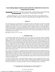
ADT flare vs. position<br />
5<br />
4.5<br />
p<br />
NXE:3100 flare vs. position<br />
Flare (%)<br />
12.5<br />
Flare (%)<br />
10.5<br />
3.5<br />
Measured<br />
8.5<br />
3<br />
Simulated<br />
6.5<br />
2.5<br />
0 2 4 6 8<br />
Position (a.u.)<br />
4<br />
Measured<br />
Simulated<br />
0 2 4 6 8<br />
Position (a.u.)<br />
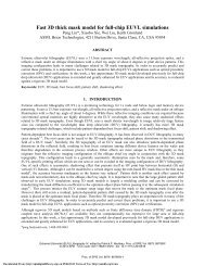
Figure 13: Measured flare data on wafer positions in the scan directions by IMEC (solid circles) vs. predicted flare values (simulated<br />
curves) at different positions on the mask. Validation was done <strong>for</strong> both the ADT as well as <strong>for</strong> the NXE:3100.<br />
6. SUMMARY<br />
We have introduced holistic <strong>lithography</strong> in <strong>EUV</strong> <strong>for</strong> the plat<strong>for</strong>m of NXE scanners: An integral approach that combines<br />
the capabilities of the NXE exposure tools with accurate predictive modeling and tailored metrology. We applied this<br />
concept to the first wafers exposed with the NXE:3100 scanners.<br />
We gave a review of the status of the NXE scanner plat<strong>for</strong>m. With now six NXE:3100 scanner shipments to the field, the<br />
year 2011 can be marked as the year that <strong>EUV</strong> made its start to integration in the FABs. Extended imaging capabilities<br />
beyond the 27-nm targets were demonstrated <strong>for</strong> flash memory, logic-SRAM and dense contact hole applications with<br />
decent process windows <strong>for</strong> 22-nm and with imaging resolution down to 18-nm.<br />
The imaging behavior of ASML’s first prototype manufacturing plat<strong>for</strong>m NXE:3100 has been modeled in detail <strong>for</strong><br />
computational <strong>lithography</strong> purposes. The model includes the optical system (pupil, slit, reflective projection lens), <strong>EUV</strong>specific<br />
flare effects (extending from short to very long-range), the <strong>EUV</strong> mask properties, and other NXE:3100 hardware<br />
components. The accuracy of the model through the image-field was demonstrated by comparing it to wafer<br />
measurements. Accurate predictive modeling of the entire image-field is of high importance <strong>for</strong> ASML’s customers to<br />
generate reliably (OPC) corrected and full-chip litho verified masks <strong>for</strong> a successful introduction of <strong>EUV</strong> to their FABs,<br />
thereby reducing learning cycles.<br />
We presented printed wafer results using a special mask that was designed by ASML and manufactured by Samsung’s<br />
captive mask shop. The mask measurements showed excellent uni<strong>for</strong>mity and quality. The mask was designed to be able<br />
to characterize the specific flare details of <strong>EUV</strong> <strong>lithography</strong> such that parameters in the model could be extracted.<br />
Furthermore, the measurements yielded in<strong>for</strong>mation on the quality of the projection optics in the NXE:3100.<br />
The wafers were measured <strong>for</strong> CD uni<strong>for</strong>mity by an ASML YieldStar S-100 scatterometry tool. After careful analysis of<br />
the large set of data, the results revealed predicted imaging effects of <strong>lithography</strong> such as flare details and residual blackborder<br />
reflections from the mask absorber stack. Furthermore, it was shown that there was no wafer CD impact caused<br />
by out-of-band DUV reflections in the NXE:3100 scanners.<br />
ACKNOWLEDGMENTS<br />
The teams of Samsung Memory and Samsung Maskshop are greatly acknowledged <strong>for</strong> their support. Gian Lorusso of<br />
IMEC is acknowledged <strong>for</strong> his cooperation on flare and permission to show the measurement data in figure 13. Fruitful<br />
interaction with ASML’s Eelco van Setten, Stuart Young, Hans Meiling, Noreen Harned and Jos Maas is greatly<br />
acknowledged. Finally, we want to thank Martin Lowisch, Martin Endres and Michael Patra of Carl Zeiss <strong>for</strong> their<br />
important contributions to modeling.<br />
Proc. of SPIE Vol. 8166 81660Z-10<br />
Downloaded From: http://proceedings.spiedigitallibrary.org/ on 04/08/2013 Terms of Use: http://spiedl.org/terms