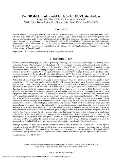
Fast 3D thick mask model for full-chip EUVL simulations
Fast 3D thick mask model for full-chip EUVL simulations - Brion ...
Fast 3D thick mask model for full-chip EUVL simulations - Brion ...
- No tags were found...

Create successful ePaper yourself
Turn your PDF publications into a flip-book with our unique Google optimized e-Paper software.
<strong>Fast</strong> <strong>3D</strong> <strong>thick</strong> <strong>mask</strong> <strong>model</strong> <strong>for</strong> <strong>full</strong>-<strong>chip</strong> <strong>EUVL</strong> <strong>simulations</strong><br />
Peng Liu*, Xiaobo Xie, Wei Liu, Keith Gronlund<br />
ASML Brion Technologies, 4211 Burton Drive, Santa Clara, CA, USA 95054<br />
ABSTRACT<br />
Extreme ultraviolet lithography (<strong>EUVL</strong>) uses a 13.5nm exposure wavelength, all-reflective projection optics, and a<br />
reflective <strong>mask</strong> under an oblique illumination with a chief ray angle of about 6 degrees to print device patterns. This<br />
imaging configuration leads to many challenges related to <strong>3D</strong> <strong>mask</strong> topography. In order to accurately predict and<br />
correct these problems, it is important to use a <strong>3D</strong> <strong>mask</strong> <strong>model</strong> in <strong>full</strong>-<strong>chip</strong> <strong>EUVL</strong> applications such as optical proximity<br />
correction (OPC) and verifications. In this work, a fast approximate <strong>3D</strong> <strong>mask</strong> <strong>model</strong> developed previously <strong>for</strong> <strong>full</strong>-<strong>chip</strong><br />
deep ultraviolet (DUV) applications is extended and greatly enhanced <strong>for</strong> EUV applications and its accuracy is evaluated<br />
against a rigorous <strong>3D</strong> <strong>mask</strong> <strong>model</strong>.<br />
Keywords: EUV, <strong>3D</strong> <strong>mask</strong>, best focus shift, pattern shift, shadowing effect<br />
1. INTRODUCTION<br />
Extreme ultraviolet lithography (<strong>EUVL</strong>) is a promising technology <strong>for</strong> 1x node and below logic and memory device<br />
patterning. It uses a 13.5nm exposure wavelength, all-reflective projection optics, and a reflective <strong>mask</strong> under an oblique<br />
illumination with a chief ray angle of about 6 degrees. While these reflective imaging conditions are required because<br />
conventional optical materials are highly absorptive at the EUV wavelength, they also cause many undesired effects<br />
related to <strong>3D</strong> <strong>mask</strong> topography. Even though <strong>EUVL</strong> uses a much shorter wavelength to image relatively large feature<br />
sizes (as compared to the wavelength) than deep ultraviolet (DUV) lithography, it actually has more <strong>3D</strong> <strong>mask</strong><br />
topography related challenges, which include pattern-dependent best focus shift, pattern shift, and shadowing effect.<br />
Pattern-dependent best focus shift is not unique to EUV lithography. It has been observed in DUV lithography in many<br />
cases already 1-3 . The root cause can be traced to the <strong>3D</strong> <strong>mask</strong> topography induced phase distortions in the transmitted<br />
field of a DUV <strong>mask</strong> 3 . Similarly, the <strong>3D</strong> topography of an EUV <strong>mask</strong> can also introduce pattern-dependent phase<br />
distortions in the reflected field, resulting in best focus variations among different device features on the wafer and<br />
there<strong>for</strong>e degradation in the common process window. Other effects are more unique to EUV lithography as they<br />
originate from the reflective imaging configuration of the oblique chief ray angle in conjunction with the <strong>3D</strong> <strong>mask</strong><br />
topography. This configuration leads to a generally asymmetric illumination seen by the <strong>mask</strong> and, there<strong>for</strong>e, some<br />
<strong>EUVL</strong>-specific printing effects which are not seen or can be avoided in the imaging configuration of DUV lithography.<br />
One of such effects is asymmetric shadowing effect that presents itself as HV print bias between horizontal (H) and<br />
vertical (V) features. Although it can be <strong>model</strong>ed to a certain degree using the rule-based HV <strong>mask</strong> bias in the thin <strong>mask</strong><br />
<strong>model</strong> 4 , the accuracy becomes inadequate as the feature size reduces 5 . Pattern shift is another such effect caused by<br />
<strong>mask</strong>-side non-telecentricity due to the oblique chief ray angle. It is important to note that the large global pattern shift<br />
observed in early EUV <strong>simulations</strong> using <strong>3D</strong> <strong>mask</strong> <strong>model</strong>s is largely a <strong>model</strong>ing artifact and can be corrected by<br />
trans<strong>for</strong>ming the <strong>mask</strong> diffraction coefficient to the optimum object plane be<strong>for</strong>e passing it to the subsequent simulation<br />
steps 4-5 . This process mimics the EUV scanner setup stage that moves the <strong>mask</strong> to the optimum <strong>mask</strong> focal plane.<br />
However there still exists a residual, pattern-dependent pattern shift caused by the <strong>3D</strong> <strong>mask</strong> topography even after the<br />
<strong>mask</strong> is placed at the optimum <strong>mask</strong> focal plane. There<strong>for</strong>e <strong>3D</strong> <strong>mask</strong> topography plays an important role in many of the<br />
challenges in EUV lithography. In order to accurately predict and correct these problems, it is important to use a <strong>3D</strong><br />
<strong>mask</strong> <strong>model</strong> in <strong>full</strong>-<strong>chip</strong> <strong>EUVL</strong> applications such as optical proximity correction (OPC) and verifications.<br />
Although rigorous <strong>3D</strong> <strong>mask</strong> <strong>model</strong>s based on methods such as finite difference time domain (FDTD) 6 and rigorous<br />
coupled wave analysis (RCWA) 7 are available, they are computationally too expensive <strong>for</strong> large area or <strong>full</strong>-<strong>chip</strong><br />
applications. In this work, a fast approximate <strong>3D</strong> <strong>mask</strong> <strong>model</strong> developed previously <strong>for</strong> <strong>full</strong>-<strong>chip</strong> DUV applications is<br />
extended and greatly enhanced <strong>for</strong> EUV applications, and its accuracy is evaluated against a rigorous <strong>3D</strong> <strong>mask</strong> <strong>model</strong>.<br />
*peng.liu@asml.com, 1-408-200-0843<br />
Extreme Ultraviolet (EUV) Lithography IV, edited by Patrick P. Naulleau, Proc. of SPIE Vol. 8679, 86790W<br />
© 2013 SPIE · CCC code: 0277-786X/13/$18 · doi: 10.1117/12.2010818<br />
Proc. of SPIE Vol. 8679 86790W-1<br />
Downloaded From: http://spiedigitallibrary.org/ on 05/06/2013 Terms of Use: http://spiedl.org/terms
In the following sections, we first discuss some special considerations in <strong>EUVL</strong> <strong>simulations</strong> with rigorous <strong>3D</strong> <strong>mask</strong><br />
<strong>model</strong>s. These considerations are required in order to obtain realistic simulation results. Then we describe the<br />
development of the fast <strong>3D</strong> <strong>mask</strong> <strong>model</strong> <strong>for</strong> <strong>full</strong>-<strong>chip</strong> EUV applications, followed by simulation case studies to validate<br />
its accuracy against a rigorous <strong>3D</strong> <strong>mask</strong> <strong>model</strong>. A summary of this work is given in the end.<br />
2. <strong>EUVL</strong> SIMULATION CONSIDERATIONS<br />
Due to limited availability of experimental data <strong>for</strong> future device dimensions, the rigorous simulation remains the main<br />
vehicle to study the various effects in EUV lithography. In this work rigorous <strong>simulations</strong> will be used to generate<br />
reference data to evaluate the accuracy of the fast <strong>3D</strong> <strong>mask</strong> <strong>model</strong>. There<strong>for</strong>e it is important to carry out the rigorous<br />
<strong>simulations</strong> properly to ensure valid results are obtained.<br />
2.1 Mask defocus effect<br />
As EUV lithography uses a reflective <strong>mask</strong> illuminated with an oblique chief ray angle, the condition of telecentricity is<br />
no longer satisfied on the <strong>mask</strong> side as compared to DUV lithography. Consequently the effects of <strong>mask</strong> defocus are<br />
much more significant in EUV lithography. This aspect is particularly evident in lithography <strong>simulations</strong> using rigorous<br />
<strong>3D</strong> <strong>mask</strong> <strong>model</strong>s. In these <strong>simulations</strong> the transmitted (DUV) or reflected (EUV) <strong>mask</strong> fields are generally sampled at a<br />
pre-determined plane close to the top surface of the <strong>mask</strong> features. If these <strong>mask</strong> fields are directly used <strong>for</strong> subsequent<br />
image <strong>simulations</strong>, which implies that the sample plane is chosen as the object plane of the project lens, the images<br />
obtained at its conjugate image plane may not be optimum in terms of image contrast and pattern shift. As shown in<br />
Figure 1, the distance between the object plane and the sample plane is referred to as the <strong>mask</strong> defocus in this work.<br />
Multi -layer<br />
ens object plane<br />
sorber<br />
Mask defocus<br />
field sample plane<br />
Figure 1: Definition of <strong>mask</strong> defocus <strong>for</strong> this work<br />
From <strong>model</strong>ing point of view, the <strong>mask</strong> defocus effect may be ignored in DUV <strong>simulations</strong>, but it cannot be ignored in<br />
EUV <strong>simulations</strong>, especially <strong>for</strong> pattern shift. Note the effect of <strong>mask</strong> defocus is similar to wafer defocus but on a much<br />
smaller scale. It can be shown that the image change due to a <strong>mask</strong> defocus of m is approximately equivalent to a wafer<br />
defocus of w =M 2 m <strong>for</strong> low NA imaging, where M is the magnification of the projection lens. For a 4x reduction<br />
system, M 2 =1/16. For CD control this effect may be ignored or largely compensated by a small change in wafer defocus.<br />
But <strong>for</strong> pattern shift, it is a quite different situation between DUV and EUV.<br />
Many factors can contribute to the image shift of a pattern with respect to its position on the <strong>mask</strong>, including pattern<br />
symmetry, source symmetry, lens aberration, phase error induced by <strong>3D</strong> <strong>mask</strong> topography, <strong>mask</strong> defocus, wafer defocus,<br />
etc... We will only consider an aberration-free system in this work. For a symmetric pattern, it can be easily shown that<br />
the pattern shift caused by the defocus and/or <strong>3D</strong> <strong>mask</strong> topography can be cancelled out exactly by using a symmetric<br />
illumination pupil shape. This condition is generally satisfied in practical DUV applications. There<strong>for</strong>e the <strong>mask</strong> defocus<br />
effect rarely needs to be <strong>model</strong>ed in DUV <strong>simulations</strong>. However, due to the reflective <strong>mask</strong> and the oblique chief ray<br />
angle employed by EUV lithography, it is impossible to make a symmetric illumination pupil shape from the <strong>mask</strong><br />
viewpoint. As a result the pattern shift in EUV is not as trivial as in DUV. The contribution from the <strong>mask</strong> defocus is<br />
significant and generally global across all patterns. In addition, a <strong>mask</strong> pattern sees a slightly different illumination pupil<br />
Proc. of SPIE Vol. 8679 86790W-2<br />
Downloaded From: http://spiedigitallibrary.org/ on 05/06/2013 Terms of Use: http://spiedl.org/terms
shape depending on its slit location. As a result, this global pattern shift on the field scale is shown as magnification error<br />
as a function of <strong>mask</strong> defocus.<br />
In practice, the global pattern shift is minimized during the scanner setup stage where the <strong>mask</strong> is driven to the optimum<br />
<strong>mask</strong> focal plane. It is important to <strong>model</strong> the same process in EUV <strong>simulations</strong> that use rigorous <strong>3D</strong> <strong>mask</strong> <strong>model</strong>s.<br />
Otherwise the resulting wafer image may show a large global pattern shift, which in reality is just a <strong>model</strong>ing artifact of<br />
not choosing the object plane properly. An example is shown in Figure 2, which compares the resist contours simulated<br />
by directly using the sample plane as the object plane to those simulated after moving the object plane to 180nm behind<br />
the sample plane. The <strong>mask</strong> <strong>simulations</strong> in this example were done using an ASML Brion in-house rigorous<br />
electromagnetic field (EMF) solver <strong>for</strong> Maxwell’s equations based on the FDTD method. A large global pattern shift of<br />
several nanometers is observed in simulation when the object plane is placed at the sample plane. But it can be corrected<br />
in simulation by moving the object plane to the optimum location, which mimics the scanner setup process.<br />
Note, <strong>for</strong> all the <strong>simulations</strong> presented in this work, an EUV system of numerical aperture NA=0.33, magnification<br />
M=0.25 and chief ray angle at object (CRAO) = 6 is used. The resist CDs and contours are computed from optical<br />
images using a constant threshold. No actual resist <strong>model</strong>s are used or required as the <strong>3D</strong> <strong>mask</strong> effects are optical effects.<br />
',ME<br />
It<br />
Object plane @ sample Iplane<br />
CD<br />
Object plane @ 180nm behind sample plane<br />
Slit location<br />
Le<br />
Illumination<br />
Bright-field<br />
image contour<br />
Dark-field<br />
image contour<br />
Figure 2: Comparison of the resist contours simulated by directly using the sample plane as the object plane (red<br />
contours) to those simulated after moving the object plane 180nm behind the sample plane (green contours)<br />
2.2 Incident angle effect<br />
In a lithography application the <strong>mask</strong> is generally illuminated by a partially coherent source. From <strong>model</strong>ing point of<br />
view, the source can be considered as a collection of planewaves, each is incoherent from others and illuminates the<br />
<strong>mask</strong> at a given incident angle. In low-NA DUV lithography <strong>simulations</strong>, the incident angle effect can be <strong>model</strong>ed using<br />
the so-called Hopkins approach, which assumes that the two transmitted fields produced by two plane waves of different<br />
angle of incidence differ by only a shift in spectral space. The diffraction order amplitude and relative phase remain the<br />
same. It is now well known that the Hopkins approach can introduce significant errors in high-NA DUV lithography<br />
<strong>simulations</strong> 8 . For the state-of-the-art DUV scanner of 1.35NA, the maximum angle of incidence on the <strong>mask</strong> is close to<br />
20 degrees. Rigorous <strong>mask</strong> <strong>simulations</strong> show that the relative phase in diffraction orders changes significantly over this<br />
range of angle of incidence. If not properly taken into account, it can produce wrong results in best focus shift<br />
predictions, which have been confirmed by both experiments and rigorous <strong>simulations</strong> 3 .<br />
The current most advanced EUV system under evaluation has NA of 0.33 and chief ray angle of 6 degrees. Figure 3<br />
shows the range of incident angle distribution on the EUV <strong>mask</strong> as compared to the DUV <strong>mask</strong>. Note the big circle in<br />
Figure 3 represents the maximum incident angle (~20 degrees) on the DUV <strong>mask</strong>. The center represents the normal<br />
incidence on the <strong>mask</strong>. The three smaller circles represent the range of the incident angle distribution on the EUV <strong>mask</strong><br />
<strong>for</strong> the slit center and two opposite edge locations, respectively. Since the incident angle distribution is much narrower<br />
on the EUV <strong>mask</strong>, it is reasonable to assume that the <strong>mask</strong> near field simulated at the chief ray angle may be<br />
Proc. of SPIE Vol. 8679 86790W-3<br />
Downloaded From: http://spiedigitallibrary.org/ on 05/06/2013 Terms of Use: http://spiedl.org/terms
epresentative enough <strong>for</strong> the entire source. This turns out to be an acceptable assumption from CD and best focus<br />
prediction point of view. But it may not be adequate <strong>for</strong> pattern shift prediction depending on the accuracy requirement.<br />
DUV<br />
(Øuv<br />
-20°<br />
Figure 3: Comparison of the range of incident angle distribution on <strong>mask</strong> between EUV and DUV<br />
A straight<strong>for</strong>ward method to <strong>model</strong> the incident angle effect of a partially coherent illumination is to decompose the<br />
illumination pupil shape into smaller sections 9 . The angle of incidence is considered constant within each section and<br />
there<strong>for</strong>e only one rigorous <strong>3D</strong> <strong>mask</strong> simulation is required to compute its contribution to the wafer image using<br />
Hopkins approach. The total wafer image is the sum of the images produced by individual sections. The result is<br />
expected to converge as the number of sections increases.<br />
A simulation work was carried out to study the convergence as a function of the number of incident angles used <strong>for</strong><br />
rigorous EUV <strong>mask</strong> <strong>simulations</strong>. The illumination pupil shape and the incident angle locations are shown in Figure 4(a).<br />
The pupil shape is the same as that shown in Figure 2 and is used to illuminate the <strong>mask</strong> at the slit edge.<br />
r1 r1 r r:<br />
Figure 4(a): Pupil shape and incident angle locations used <strong>for</strong> rigorous <strong>3D</strong> <strong>mask</strong> <strong>simulations</strong><br />
We investigated both bright-field and dark-field <strong>mask</strong>s having horizontal (H) and vertical (V) lines or spaces of<br />
width=12nm and pitch=100nm on wafer scale. The simulation was done using HyperLith’s RCWA-based rigorous <strong>3D</strong><br />
<strong>mask</strong> <strong>model</strong>. We pre-scanned the <strong>mask</strong> defocus and selected a value to minimize the global patterns shift. This value was<br />
then fixed <strong>for</strong> all the <strong>simulations</strong>. Figure 4(b) shows the results of Bossung curves of XCD (CD of V line/space) and<br />
YCD (CD of H line/space). It is apparent that the number of angles has very small effect on CD and best focus shift. One<br />
angle of incidence at the chief ray may be considered adequate. It is also worth noting that the best focus shift is patterndependent<br />
between horizontal and vertical features, caused by <strong>3D</strong> <strong>mask</strong> topographies.<br />
Bright Field X & Y Bossung<br />
-100 -80 -60 -40 -20 0 20 40<br />
Wager Faune, nm<br />
60 80 100<br />
zcD_Mngles=l<br />
-XCD_Mngles=2<br />
-XCO_nAngles=4<br />
-XCD_nangles=12<br />
- XCD nAngles=l6<br />
-Y,11D_ A gl -<br />
-YCO_nAngles=2<br />
-0C11_44n0es=4<br />
- YCD Mngles=l2<br />
-YCD_Mngles=l6<br />
Dark Field X & Y Bossung<br />
-100 -80 -60 -40 -20 0 20 40 60<br />
Miler Foam, M<br />
80 100<br />
-XCO Mngles=l<br />
X00_44444=2<br />
XC0_nAngles=4<br />
XCD_nAndes=12<br />
-XCD_nAn41es=16<br />
-YCD_Mngles=l<br />
-1CD_Mngles=2<br />
-YCD_Mngles=4<br />
-VCD_Mngles=l2<br />
-YCD_Mngles=16<br />
Figure 4(b): Convergence of Bossung curve as a function of the number of incident angles used <strong>for</strong> rigorous <strong>3D</strong><br />
<strong>mask</strong> <strong>simulations</strong>. XCD = CD of V line/space. YCD = CD of H line/space.<br />
Proc. of SPIE Vol. 8679 86790W-4<br />
Downloaded From: http://spiedigitallibrary.org/ on 05/06/2013 Terms of Use: http://spiedl.org/terms
Y Shift<br />
I<br />
Bright Field X & Y Shift thru Focus<br />
-Xshi t_nAnglesl<br />
X Shift<br />
-100 -80 -60 -40 -20 0 20 40 60 80 100<br />
wafeewas, nm<br />
-Xshift-nAngles =2<br />
Xshi t_nAngles4<br />
Xshift_nAnglesl2<br />
-Xshif[_nAngles16<br />
-Yshift _nAnelesl<br />
-Yshift_nAngles2<br />
-YshitLnAngles4<br />
-Yshift_nAngles12<br />
-YshilLnAngles16<br />
i<br />
C<br />
Dark Field X & Y Shift thru Focus<br />
Y Shift<br />
woji<br />
- 100 -80 -60 -40 -20 0 20 40 60 80 100<br />
Wafer Focus, mit<br />
-Xshift_nAndes=l<br />
-Xshift_nnndes=2<br />
-Xshift_nAngles4<br />
Xsliift_nAngles12<br />
-Xshift-nAngles=l6<br />
-Yshift-nAnglesl<br />
YshiR_nAngles=2<br />
-YShift _Mngles4<br />
-Yshi(t_Mnglesl2<br />
-YshilLMngles16<br />
Figure 4(c): Convergence of thru-focus pattern shift as a function of the number of incident angles used <strong>for</strong><br />
rigorous <strong>3D</strong> <strong>mask</strong> <strong>simulations</strong>. X Shift = pattern shift of V line/space. Y Shift = pattern shift of H line/space<br />
The convergence is however quite different <strong>for</strong> pattern shift. As shown in Figure 4(c), using only the chief ray angle can<br />
cause over 1nm error in pattern shift prediction and incorrect thru-focus trend. At least two incident angles, one <strong>for</strong> each<br />
pole, are required to reduce the error to below 0.5nm and to obtain the correct trend. More are needed to further reduce<br />
the error. But it is not going to be very practical <strong>for</strong> 2D pattern <strong>simulations</strong> as they are very time consuming. In this<br />
example, up to 12 incident angles may be required to obtain a near converged result.<br />
3. FAST <strong>3D</strong> MASK MODEL DEVELOPMENT<br />
In this section we describe the extension and enhancement of a fast approximate <strong>3D</strong> <strong>mask</strong> <strong>model</strong> <strong>for</strong> <strong>full</strong>-<strong>chip</strong> EUV<br />
applications. This <strong>model</strong> was developed previously <strong>for</strong> <strong>full</strong>-<strong>chip</strong> DUV applications and showed good accuracy in best<br />
focus shift predictions as compared to rigorous <strong>model</strong>s and experiments 3 . The details of its development are given in the<br />
previous work 10 and there<strong>for</strong>e not repeated here. In the following discussions, we first summarize the key elements of the<br />
previous <strong>model</strong> as they are the foundation of the present work. Then we describe the additional development made in<br />
this work to extend it <strong>for</strong> <strong>full</strong>-<strong>chip</strong> EUV applications.<br />
Figure 5: Illustration of the working principle of the fast <strong>3D</strong> <strong>mask</strong> <strong>model</strong><br />
As discussed in our previous work, the fast <strong>3D</strong> <strong>mask</strong> <strong>model</strong> developed <strong>for</strong> DUV lithography consists of the following<br />
key elements. First of all, the <strong>mask</strong> image of a given pattern is computed by convolving the layout properties such as<br />
polygon area and edges with the so-called M<strong>3D</strong> filters. This process is illustrated in Figure 5. For a coherent illumination<br />
Proc. of SPIE Vol. 8679 86790W-5<br />
Downloaded From: http://spiedigitallibrary.org/ on 05/06/2013 Terms of Use: http://spiedl.org/terms
this <strong>mask</strong> image is directly related to the transmitted field of the <strong>mask</strong>. For a partially coherent illumination it does not<br />
have a direct association with a measureable physical property. It is more of an intermediate mathematical property that<br />
is to be convolved with the Transmission Cross Coefficient (TCC) of Hopkins theory to obtain the wafer image.<br />
There<strong>for</strong>e the <strong>model</strong> accuracy is determined by the <strong>mask</strong> image and in turn by the M<strong>3D</strong> filters. We construct these filters<br />
from a library of transmitted fields of representative <strong>mask</strong> features, pre-computed using a rigorous EMF solver <strong>for</strong><br />
Maxwell’s equations. The use of a rigorous EMF solver ensures that the relative phase between diffraction orders can be<br />
captured besides amplitude. Note this phase in<strong>for</strong>mation is completely missing in the thin <strong>mask</strong> <strong>model</strong> but plays an<br />
important role in determining the best focus of a given pattern. In addition, the relative phase greatly depends on the<br />
incident angle. In order to capture this dependency, an array of transmitted fields of various incident angles needs to be<br />
included in the rigorous library <strong>simulations</strong>. Then, <strong>for</strong> a given partially coherent illumination, we combine these rigorous<br />
library fields according to its pupil shape to compute the filters. The oblique incidence effect is thus embedded in these<br />
filters. One set of filters can be computed <strong>for</strong> the entire pupil or a sub-section of the pupil depending on the accuracy<br />
requirement. In a <strong>full</strong>-<strong>chip</strong> simulation these filters are re-used to compute the <strong>mask</strong> images <strong>for</strong> each patch of <strong>mask</strong><br />
patterns.<br />
It has been shown that the above <strong>model</strong> is capable of accurately predicting the best focus shift observed in rigorous<br />
<strong>simulations</strong> and experiments in DUV applications. In this work, it is further extended and enhanced <strong>for</strong> EUV<br />
applications. It is referred to as M<strong>3D</strong>+ <strong>model</strong> in this work as opposed to the previous M<strong>3D</strong> <strong>model</strong>. The basic working<br />
principle of this <strong>model</strong> stays the same as shown in Figure 5. The new developments are mainly in the area of M<strong>3D</strong>+<br />
filter generation that takes into account <strong>mask</strong> defocus effect and edge-to-edge interaction effect. These new<br />
developments are illustrated in Figure 6, followed by more detailed discussions on each of the components.<br />
Figure 6: Illustration of M<strong>3D</strong>+ filter generation <strong>for</strong> <strong>EUVL</strong> <strong>simulations</strong><br />
3.1 Library generation <strong>for</strong> EUV <strong>mask</strong><br />
EUV lithography uses a reflective <strong>mask</strong> as opposed to a transmissive <strong>mask</strong> in DUV lithography. There<strong>for</strong>e, instead of<br />
transmitted fields, the reflected fields of representative EUV <strong>mask</strong> features need to be rigorously simulated and stored in<br />
the library. The reflected fields at various incident angles, not just the chief ray angle, are also required in order to<br />
capture the incident angle effect of a partially coherent source in EUV lithography.<br />
3.2 Mask defocus<br />
As discussed in the previous section, the <strong>mask</strong> defocus has a significant effect on the results of EUV <strong>simulations</strong> with <strong>3D</strong><br />
<strong>mask</strong> <strong>model</strong>s. It is important to <strong>model</strong> the scanner setup process that moves the <strong>mask</strong> to the optimum <strong>mask</strong> focal plane.<br />
To enable this capability, the previous fast <strong>3D</strong> <strong>mask</strong> <strong>model</strong> is extended to include the <strong>mask</strong> defocus function. It is<br />
implemented by first propagating the library fields from the sample plane to the object plane as specified by the <strong>mask</strong><br />
defocus and then constructing the filters from the new library fields. Note that, since the <strong>mask</strong> defocus effect is included<br />
in the filters, there is no runtime impact in OPC and verification applications. The optimum <strong>mask</strong> defocus can be<br />
determined by mimicking the scanner setup process that minimizes the global pattern shift.<br />
Proc. of SPIE Vol. 8679 86790W-6<br />
Downloaded From: http://spiedigitallibrary.org/ on 05/06/2013 Terms of Use: http://spiedl.org/terms
3.3 Edge-to-edge interaction<br />
From <strong>model</strong>ing point of view, the total EMF scattering effect of a <strong>mask</strong> may be separated into two parts – the primary<br />
scattering effect and the secondary scattering effect. The <strong>for</strong>mer refers to the EMF scattering effect of individual feature<br />
edges, including the interference effect of these individually scattered fields. The latter refers to the interaction effect that<br />
a scattered field being scattered again by nearby edges and so on. The secondary scattering effect is usually much<br />
smaller than the primary scattering effect. It may be ignored in many cases where the edge separation is large and/or the<br />
feature height is small so that the interaction is weak.<br />
As the device feature sizes continue to shrink, the <strong>model</strong>ing errors introduced by edge-to-edge interactions begin to show<br />
appreciable impact to the CD and overlay error budget. This effect is particularly apparent <strong>for</strong> EUV lithography because<br />
the absorber height is much larger than the wavelength and comparable to the spaces of dense features, making it more<br />
susceptible to interactions with the scattered fields from neighboring edges. The edge-to-edge interaction effect in EUV<br />
<strong>mask</strong> may be conceptually illustrated in Figure 7(a), where the largest arrow represents the incident field and the smaller<br />
solid arrows represent the primary scattered field from the left edge. Part of this scattered field hits the nearby right edge<br />
and is scattered again, resulting in a secondary scattered field.<br />
S<br />
Figure 7(a): Conceptual illustration of edge-toedge<br />
interaction in EUV <strong>mask</strong><br />
8 -<br />
7 -<br />
6 -<br />
5 -<br />
4 -<br />
3 -<br />
2 -<br />
1 -<br />
0<br />
1<br />
10<br />
Horizontal space CD error<br />
as a function of absorber space width<br />
- M<strong>3D</strong>+<br />
- M<strong>3D</strong><br />
15 20 25 30<br />
S @ wafer scale (nm)<br />
Illumination<br />
Figure 7(b): Model accuracy comparison between<br />
M<strong>3D</strong> (w/o edge-to-edge interaction effect taken<br />
into account) and M<strong>3D</strong>+ (w/ interaction effect<br />
taken into account)<br />
In this work we have extended the previous <strong>model</strong> by adding rigorous <strong>simulations</strong> of edge interaction fields as part of the<br />
library generation. These additional library fields enable us to extract the edge-to-edge interaction effect and build<br />
additional filters. By applying these filters we are able to include the edge-to-edge interaction effect in <strong>full</strong>-<strong>chip</strong> <strong>EUVL</strong><br />
<strong>simulations</strong>.<br />
A simulation example is shown in Figure 7(b) which compares the <strong>model</strong> accuracy as a function of absorber space<br />
between the M<strong>3D</strong> <strong>model</strong> (w/o the edge-to-edge interaction effect taken into account) and the M<strong>3D</strong>+ <strong>model</strong> (with the<br />
interaction effect taken into account). The CD error refers to the difference between the CD predicted by the<br />
M<strong>3D</strong>/M<strong>3D</strong>+ <strong>model</strong> and that by the rigorous FDTD <strong>model</strong>. As the space becomes smaller than 17nm (wafer scale), the<br />
M<strong>3D</strong> CD error starts to increase significantly while M<strong>3D</strong>+ maintains an excellent accuracy. The pitch is fixed at 100nm<br />
in this example. More accuracy evaluations on the M<strong>3D</strong>+ <strong>model</strong> are discussed in the next section.<br />
Note the above method <strong>for</strong> edge-to-edge interaction <strong>model</strong>ing is not limited to <strong>EUVL</strong>, it can be used <strong>for</strong> DUV<br />
<strong>simulations</strong> as well.<br />
4. MODEL ACCURACY VALIDATION<br />
In this section we evaluate the accuracy of the fast <strong>3D</strong> <strong>mask</strong> <strong>model</strong> against rigorous results <strong>for</strong> <strong>EUVL</strong> <strong>simulations</strong>. Two<br />
case studies were carried out, one on 1D patterns and the other on 2D patterns. The in-house FDTD EMF solver was<br />
used to generate the reference data <strong>for</strong> these studies as it is more memory efficient than RCWA <strong>for</strong> 2D pattern<br />
<strong>simulations</strong>. The benchmark between these two rigorous EMF solvers showed good agreement <strong>for</strong> the 1D test case<br />
presented in Section 2. The comparison is shown below in Figure 8.<br />
Proc. of SPIE Vol. 8679 86790W-7<br />
Downloaded From: http://spiedigitallibrary.org/ on 05/06/2013 Terms of Use: http://spiedl.org/terms
Bright Field X & Y Bossung<br />
Dark Field X & Y Bossung<br />
XCD<br />
YCD<br />
XCDRCWA<br />
XCDFDID<br />
YCD RCWA<br />
-YCD FDID<br />
XCD<br />
/1111YCD<br />
XCDRCWA<br />
-XCDFDID<br />
-YCDRCWA<br />
-YCD FDID<br />
-100 -80 -60 -40 -20 0 20 40 60 80 100<br />
Wafer Pause, nm<br />
-100 -80 -60 -40 -20 0 20 40 60 80 100<br />
Wafer Focus, nm<br />
Bright Field X & Y Shift thru Focus<br />
Dark Field X & Y Shift thru Focus<br />
X Shift<br />
Y Shift<br />
-Xshlft RCWA<br />
-Wilk FIND<br />
-Yshift RCWA<br />
-YshBtFDTD<br />
s<br />
X Shift<br />
Y Shift<br />
-XShiftRCWA<br />
-XshiftFDTD<br />
-YshIft RCWA<br />
-Yshift FDlD<br />
-100 -80 40 -M -20 0 20 90 60 80 100<br />
Wafer roan, n<br />
-100 -80 40 -40 -20 0 20 90 60 80 100<br />
Wafer For. mr<br />
Figure 8: Comparison of simulation results between RCWA and FDTD<br />
In the following discussions we present the comparison between the fast <strong>3D</strong> <strong>mask</strong> <strong>model</strong> M<strong>3D</strong>+ and the rigorous <strong>3D</strong><br />
<strong>mask</strong> <strong>model</strong> FDTD. The comparison to thin <strong>mask</strong> <strong>model</strong> is also included as appropriate.<br />
4.1 1D pattern case study<br />
The 1D patterns used in this study consist of H/V lines (<strong>for</strong> bright-field <strong>mask</strong>) or spaces (<strong>for</strong> dark-field <strong>mask</strong>) of width<br />
from 10nm to 30nm, pitch from 28nm to 40nm with 2nm increment and from 40nm to 100nm with 10nm increment.<br />
Rigorous <strong>simulations</strong> were done first to generate the reference CD data <strong>for</strong> a range of focus-exposure matrix (FEM)<br />
conditions. The H and V line/space CD’s of the largest feature (i.e., 30nm lines or spaces with 100nm pitch) at the center<br />
slit location under the nominal FEM condition were used to calibrate the threshold of the M<strong>3D</strong>+ <strong>model</strong>. A thin <strong>mask</strong><br />
<strong>model</strong> was also calibrated, which included HV <strong>mask</strong> bias in addition to threshold. The calibrated <strong>model</strong> was then used to<br />
predict CDs and pattern shift of all features at both center and edge slit locations under the <strong>full</strong> range of FEM conditions.<br />
The results were compared with the rigorous reference data.<br />
Figure 9 shows the M<strong>3D</strong>+ and thin <strong>mask</strong> <strong>model</strong> RMS of predicted CD delta to rigorous FDTD <strong>model</strong>. The RMS was<br />
calculated across all features per slit location, FEM condition and <strong>mask</strong> type. The prediction power is significantly<br />
improved by the M<strong>3D</strong>+<strong>model</strong> over the thin <strong>mask</strong> <strong>model</strong>.<br />
The issue with the thin <strong>mask</strong> <strong>model</strong> is the lack of the prediction capability <strong>for</strong> pattern-dependent best focus shift and HV<br />
bias. An example is given in Figure 10, which compares the Bossung curves between the thin <strong>mask</strong> <strong>model</strong> and FDTD <strong>for</strong><br />
12nm and 30nm lines/spaces having 100nm pitch under the nominal dose condition. Clearly, the thin <strong>mask</strong> fails to<br />
capture the pattern-dependent best focus shift. In addition, the HV <strong>mask</strong> bias that works <strong>for</strong> large features fails to work<br />
<strong>for</strong> small features, particularly <strong>for</strong> the dark-field <strong>mask</strong>.<br />
The M<strong>3D</strong>+ is not shown in Figure 10 because it is on top of FDTD almost exactly in this example. More detailed<br />
Bossung comparisons between M<strong>3D</strong>+ and FDTD are given in Figures 11(a-d).<br />
The comparison of pattern shift between M<strong>3D</strong>+ and FDTD is shown in Figures 12(a-c). Thin <strong>mask</strong> <strong>model</strong> is not shown<br />
as it cannot capture this effect.<br />
Proc. of SPIE Vol. 8679 86790W-8<br />
Downloaded From: http://spiedigitallibrary.org/ on 05/06/2013 Terms of Use: http://spiedl.org/terms
I<br />
I<br />
7<br />
6<br />
5<br />
4<br />
3<br />
2<br />
1<br />
0<br />
7<br />
6<br />
5<br />
4<br />
3<br />
2<br />
1<br />
0<br />
7<br />
6<br />
5<br />
4<br />
3<br />
2<br />
1<br />
0<br />
I<br />
Prediction RMS (CD delt1 to FDTP)<br />
rirhi l.\ :l.ltl\l\ :lt.ltLtAl.11lr. rnnr,r Rrirvht finl clii orJrvo<br />
M<strong>3D</strong>+<br />
rT<br />
THIN<br />
1 1<br />
II<br />
is<br />
1 1 1 1 ,<br />
-80-60-40-20 0 20 40 60 80 80-60-40-20 0 20 40 60 8 80-60-40-20 0 20 40 60<br />
.<br />
1111/<br />
. . . . .<br />
1.11111<br />
-80-60-40-20 0 20 40 60 80<br />
Focus (nm)<br />
- . -<br />
80-60-40-20 0 20 40 60<br />
Focus (nm)<br />
-<br />
-<br />
- -<br />
-80-60-40-20 0 20 40 60 80 80-60-40-20 0 20 40 60 8<br />
8<br />
-<br />
.<br />
ronrlr..\llJl<br />
ll.11lm. 1.llJ- '- a,<br />
1<br />
1<br />
1<br />
80 80-60-40-20 0 20 40 60 80<br />
80-60-40-20 0 20 40 60 80 80-60-40-20 0 20 40 60 80<br />
Focus (nm)<br />
Focus (nm)<br />
- -<br />
-<br />
-<br />
1 II<br />
1<br />
-<br />
-<br />
80-60-40-20 0 20 40 60 80 80-60-40-20 0 20 40 60 80<br />
I<br />
-<br />
-<br />
!MENU<br />
Figure 9: M<strong>3D</strong>+ and thin <strong>mask</strong> <strong>model</strong> RMS of predicted CD delta to FDTD. The RMS was calculated across all<br />
features per slit location, FEM condition and <strong>mask</strong> type. The issue with the thin <strong>mask</strong> <strong>model</strong> is the lack of the<br />
prediction capability <strong>for</strong> pattern-dependent best focus shift and HV bias (see Figure 10).<br />
Comparison of Bossung between thin <strong>mask</strong> and FDTD<br />
Anchor<br />
nchor<br />
50<br />
40<br />
E<br />
g 30<br />
v<br />
20<br />
10<br />
o<br />
°0ó 7°78<br />
1<br />
° ° ° ° ° ° v<br />
mQtl._ 7'J-6!)<br />
° ° °<br />
/-<br />
00000 o<br />
° ° °<br />
g<br />
.0<br />
p.<br />
87°.783<br />
. . . . . . . .. . . . .<br />
-H - FDTD<br />
o H -THIN<br />
-V - FDTD<br />
o V-THIN<br />
4- Focus(nm)<br />
12<br />
30 12<br />
30<br />
12<br />
30<br />
12<br />
30<br />
F Width (nm)<br />
100<br />
100<br />
100<br />
100<br />
F Pitch (nm)<br />
Center<br />
Bright Field<br />
Edge<br />
Center<br />
Dark Field<br />
Edge<br />
F Slit Loc<br />
E- Mask Type<br />
Figure 10: Comparison of Bossung curves between thin <strong>mask</strong> <strong>model</strong> and FDTD under the nominal dose condition. The<br />
thin <strong>mask</strong> fails to capture the pattern-dependent best focus shift. In addition, the HV bias that works <strong>for</strong> large features<br />
in the thin <strong>mask</strong> <strong>model</strong> fails to work <strong>for</strong> small features, particularly <strong>for</strong> the dark-field <strong>mask</strong>.<br />
Proc. of SPIE Vol. 8679 86790W-9<br />
Downloaded From: http://spiedigitallibrary.org/ on 05/06/2013 Terms of Use: http://spiedl.org/terms
Bright field thru -pitch Bossung of 12nm line at slit center<br />
25<br />
20<br />
E<br />
C 15<br />
e<br />
10<br />
r r<br />
á<br />
-XCD-FDTD<br />
O XCD-M<strong>3D</strong>+<br />
-YCD - FDTD<br />
o YCD-M<strong>3D</strong>+<br />
s<br />
O<br />
-80 O iI-40401111 0 Zi-0090-f11 0 all -004010 0
30<br />
Dark field thru -pitch Bossung of 12nm space at slit edge<br />
25<br />
20<br />
E<br />
= 15<br />
V<br />
10<br />
fIA"<br />
.. -,.i &901(41410)<br />
-XCD - FDTD<br />
o XCD- M<strong>3D</strong>+<br />
YCD - FDTD<br />
o YCD -M 3 D+<br />
-80 0 80 -40 40 -80 0 80 -40 40 -80 0 80 -4040 -80 0 80 -40 40 -80 0 80 -40 40 -80 0 80 -40 40<br />
4- Focus (nm)<br />
30 32 34 36 38<br />
40 50 60 70<br />
80 90 100<br />
4- Pitch (nm)<br />
Figure 11(d): Dark field thru-pitch Bossung of 12nm space at slit edge under the nominal dose condition<br />
1.5<br />
Thru -pitch thru -focus Y pattern shift of<br />
12nm line /space at slit center<br />
1<br />
E<br />
e 0.5<br />
s<br />
rn<br />
o<br />
e<br />
8 -0.5<br />
á<br />
6<br />
1<br />
-Bright Field - FDTD<br />
o Bright Field - M<strong>3D</strong>+<br />
-Dark Field - FDTD<br />
o Dark Field - M<strong>3D</strong>+<br />
1.5<br />
-80 0 80-4040<br />
30 32<br />
346 3840 5060 so 7080 9000 1
I<br />
Dark field thru -pitch thru -focus pattern shift of<br />
12nm space at slit edge<br />
2.5<br />
2<br />
E 15<br />
c<br />
t 0.5<br />
tn c 0<br />
-X Shift -FDTD<br />
o X Shift -M<strong>3D</strong>+<br />
-V Shift -FDTD<br />
o V_Shift -M<strong>3D</strong>+<br />
-2<br />
0 80-4040 -d0 0 80-4040 -do 0 80-4040 -80 0 80-4040 -80 0 80-4040 -d0 0 80-4040<br />
30 32 34 36 38 40 50 60 70 80 90 100<br />
F Focus (nm)<br />
F Pitch (nm)<br />
Figure 12(c): Dark field thru-pitch thru-focus pattern shift of 12nm space at slit edge under the nominal dose condition<br />
4.2 2D pattern case study<br />
2D patterns of an actual design are much more diverse compared to 1D patterns. To make this study more relevant, we<br />
adopted the 2D patterns previously investigated by a device manufacturer, which highlighted the need of <strong>3D</strong> <strong>mask</strong><br />
<strong>model</strong>ing in EUV applications 11 . These patterns are shown in Figure 13.<br />
EX1 (anchor)<br />
00<br />
D °° D<br />
CC<br />
0 0<br />
0 0 0 0<br />
0 0<br />
0 0<br />
° ° ° °<br />
° ' °<br />
0 0 00 0<br />
O° 0 0 0 0 0<br />
DC DO 0<br />
x 14nm<br />
0$ 22nm o 0 0<br />
0 0 0 0<br />
0 0 0<br />
0 0<br />
0 0<br />
° ° °<br />
EX2oo<br />
o 0 0<br />
0 0 2 nm x 14n<br />
0 0 0 0 0<br />
0 0 0<br />
0 0 0 0 0<br />
CC 0<br />
00 0<br />
° ° ° °<br />
EX4A<br />
EX16<br />
0 0<br />
0 0<br />
D O C C<br />
0 0<br />
Do<br />
13nmx26n,<br />
] 0-9-0 0<br />
0 0 0 0<br />
1 0 0 0 0<br />
Figure 13: 2D patterns used in simulation<br />
l0000000<br />
0 0 0 0 0<br />
22nm x 14nm<br />
0-12- o 0 0<br />
O C C<br />
0 0<br />
O C O O<br />
0 0 0<br />
The size of the feature at the simulation domain center is labeled. In this work these patterns were directly used in<br />
<strong>simulations</strong> without any OPC. Again, rigorous <strong>simulations</strong> were done first to generate reference data. The X- and Y-<br />
CD’s of the first pattern (EX1) at the slit center under the nominal FEM condition were used to calibrate the M<strong>3D</strong>+<br />
<strong>model</strong> and the thin <strong>mask</strong> <strong>model</strong>. Only threshold was calibrated <strong>for</strong> the M<strong>3D</strong>+ <strong>model</strong>. For the thin <strong>mask</strong> <strong>model</strong>, HV bias<br />
was also calibrated in addition to threshold. Then the calibrated <strong>model</strong> was used to predict the printed contours of all<br />
patterns and compared to rigorous results. The RMS of predicted CD delta to FDTD is shown in Figure 14.<br />
Proc. of SPIE Vol. 8679 86790W-12<br />
Downloaded From: http://spiedigitallibrary.org/ on 05/06/2013 Terms of Use: http://spiedl.org/terms
Prediction F" IS (CD delta to FDTD)<br />
M<strong>3D</strong>+<br />
ETHIN<br />
IThT1111I. 000<br />
O O O O O Ñ<br />
Otzt<br />
O<br />
Oo tD O<br />
00<br />
O<br />
lD<br />
O<br />
q N<br />
O O O<br />
N Q<br />
O<br />
ID<br />
O<br />
00<br />
O<br />
Focus (nm)<br />
Focus (rim)<br />
ocus nm<br />
_ _ -1<br />
0 0 0 O<br />
0 0 D o e<br />
4 N N O o Sr tD O O O 00 Op q N N<br />
Focus (nm)<br />
Focus (nm)<br />
I r10,<br />
00 tD O N O N Q tD co<br />
, q<br />
Figure 14: M<strong>3D</strong>+ and thin <strong>mask</strong> <strong>model</strong> RMS of predicted CD delta to FDTD. The RMS was calculated across all<br />
features per slit location, FEM condition and <strong>mask</strong> type. One pattern was removed from the thin <strong>mask</strong> dark-field<br />
RMS calculation as it was not printed under the thin <strong>mask</strong> <strong>model</strong> (some thin <strong>mask</strong> <strong>model</strong> data points under offnominal<br />
conditions were also removed <strong>for</strong> the same reason).<br />
Note one pattern was removed from the thin <strong>mask</strong> dark-field RMS calculation as it was not printed under the thin <strong>mask</strong><br />
<strong>model</strong> (some thin <strong>mask</strong> <strong>model</strong> data points under off-nominal conditions were also removed <strong>for</strong> the same reason). But it<br />
was printed in the FDTD <strong>model</strong>. As shown in Figure 15 which compares the Bossung between thin <strong>mask</strong> and FDTD, the<br />
thin <strong>mask</strong> <strong>model</strong> CD of EX4B is reported as zero since the pattern fails to print. The dark-field <strong>mask</strong> generally has lower<br />
image quality, especially when without OPC, and there<strong>for</strong>e a small error in image can result in a large error in contour<br />
defined by threshold. For the same reason, the M<strong>3D</strong>+ <strong>model</strong> RMS is worse on the dark-field <strong>mask</strong> than the bright-field<br />
<strong>mask</strong>, although it is significantly improved over the thin <strong>mask</strong> <strong>model</strong>. More detailed comparisons between M<strong>3D</strong>+ and<br />
FDTD are given in Figure 16 on Bossung curves and in Figure 17 on pattern shift.<br />
50<br />
45<br />
40<br />
35<br />
o<br />
E<br />
C 25<br />
è<br />
' 20<br />
5<br />
10<br />
Dark field Bossung comparison between THIN and FDTD<br />
\<br />
o o<br />
-%CD-FDTD<br />
o %CD-THIN<br />
-Ym -FDTD<br />
o Ym-THIN<br />
5<br />
o<br />
®m..r<br />
o ao -ao ao o 80 -40 ao -b o w eo ao 0 -40 90 0 80 -40 e0 0 10 40 (- Focus Om)<br />
03<br />
cntr<br />
E%CA EMa EIWC Ex1 018 EQ Ex9<br />
Dark Field<br />
eaEe<br />
EMA EMS EMC - Vattern<br />
c-Slit Loe<br />
4-Mask Type<br />
Figure 15: Dark field Bossung comparison between thin <strong>mask</strong> and FDTD under the nominal dose condition. Note<br />
the thin <strong>mask</strong> <strong>model</strong> CD of EX4B is reported as zero since the pattern fails to print. It was removed from the thin<br />
<strong>mask</strong> <strong>model</strong> RMS calculation.<br />
Proc. of SPIE Vol. 8679 86790W-13<br />
Downloaded From: http://spiedigitallibrary.org/ on 05/06/2013 Terms of Use: http://spiedl.org/terms
Bright field Bossung comparison between M<strong>3D</strong>+ and FDTD<br />
Figure 16(a): Bright field Bossung comparison between M<strong>3D</strong>+ and FDTD under the nominal dose condition<br />
Dark field Bossung comparison between M<strong>3D</strong>+ and FDTD<br />
50<br />
45<br />
40<br />
E<br />
gs<br />
8 20<br />
B<br />
-.1'.i1' -<br />
46. .<br />
>ivaccisc#2'<br />
-%CD - FDTD<br />
o %CD-M<strong>3D</strong>t<br />
-YCD-FDTD<br />
o YCD-M<strong>3D</strong>+<br />
io<br />
s<br />
o<br />
40 0 -0040 40 0 8o4040 -0 0 -40 40<br />
E%1 sae EX1 EKB DNA DAB<br />
cnti<br />
0 804040 0 4040 0 lI 4040<br />
E%CC EA EIOB Egl EIEI l E%W<br />
edge<br />
Dark Field<br />
0 g04000<br />
EXOB<br />
E%OC<br />
Figure 16(b): Dark field Bossung comparison between M<strong>3D</strong>+ and FDTD under the nominal dose condition<br />
1.5<br />
Bright field thru -pitch pattern shift comparison between M<strong>3D</strong>+ and FDTD<br />
1<br />
E 0.5<br />
o<br />
m -05<br />
a<br />
..-<br />
o<br />
I.<br />
. .o<br />
i..<br />
v.<br />
...<br />
--- -::-<br />
' :. -<br />
--. .: .......<br />
........<br />
. i.,. ,....<br />
.._ _<br />
-.<br />
o<br />
-XShift - FDTD<br />
o XShift-M<strong>3D</strong>+<br />
-YSh ift - FDTD<br />
o YShift-M<strong>3D</strong>+<br />
1.5<br />
to o 80 -40 40 -do 0 80 -40 40 -do 0 80 -40 40 -d0 0 80 -40 40 -do 0 80 -40 40 -do 0 80 -40 40 -do 0 80 -40 40<br />
EX1<br />
EX1B<br />
EX2<br />
EX3<br />
EX4A<br />
EX4B<br />
EX4C<br />
EX1<br />
EX1B<br />
EX2<br />
EX3<br />
EX4A<br />
EX4B<br />
EX4C<br />
cntr<br />
Bright Field<br />
edge<br />
Figure 17(a): Bright field pattern shift comparison between M<strong>3D</strong>+ and FDTD under the nominal dose condition<br />
Proc. of SPIE Vol. 8679 86790W-14<br />
Downloaded From: http://spiedigitallibrary.org/ on 05/06/2013 Terms of Use: http://spiedl.org/terms
2<br />
1.5<br />
E<br />
t<br />
0.5<br />
rn<br />
E. o<br />
á -0.5<br />
-1<br />
-1.5<br />
Dark field thru -pitch pattern shift comparison between M<strong>3D</strong>+ and FDTD<br />
_<br />
o<br />
.. _, .... ,..<br />
----'°- -- - '---<br />
O O ..,<br />
o<br />
o<br />
o<br />
:<br />
... .... ..<br />
%<br />
30 0 80 -40 40 -8,0 0 80 -40 40 -8,0 0 80 -40 40 -80 0 80 -40 40 -80 0 80 -40 40 -8,0 0 80 -40 40 -80 0 80 -40 40<br />
-XShift - FDTD<br />
o XShift - M<strong>3D</strong>+<br />
-YShift - FDTD<br />
o YShift-M<strong>3D</strong>+<br />
EX1<br />
EX1B<br />
EX2<br />
EX3<br />
EX4A<br />
EX4B<br />
EX4C<br />
EX1<br />
EX1B<br />
EX2<br />
EX3<br />
EX4A<br />
EX4B<br />
EX4C<br />
cntr<br />
edge<br />
Dark Field<br />
Figure 17(b): Dark field pattern shift comparison between M<strong>3D</strong>+ and FDTD under the nominal dose condition<br />
5. SUMMARY<br />
We have discussed the special considerations on <strong>mask</strong> defocus and incident angle effects in rigorous <strong>EUVL</strong> <strong>simulations</strong><br />
using <strong>3D</strong> <strong>mask</strong> <strong>model</strong>s. The optimum <strong>mask</strong> defocus needs to be determined first by mimicking the scanner setup process<br />
so that the global pattern shift or magnification error is minimized. Unlike in DUV <strong>simulations</strong>, the incident angle has<br />
only a small effect on CD and best focus prediction in EUV <strong>simulations</strong>. But it has a significant impact to pattern shift<br />
prediction.<br />
In this work we have extended and enhanced a fast <strong>3D</strong> <strong>mask</strong> <strong>model</strong> developed previously <strong>for</strong> <strong>full</strong>-<strong>chip</strong> DUV applications<br />
to EUV applications. The new development includes <strong>model</strong>ing of <strong>mask</strong> defocus and edge-to-edge interaction effects.<br />
Case studies were carried out to evaluate its accuracy against a rigorous <strong>3D</strong> <strong>mask</strong> <strong>model</strong> <strong>for</strong> 1D and 2D patterns in both<br />
bright-field and dark-field <strong>mask</strong>s. The fast <strong>3D</strong> <strong>mask</strong> <strong>model</strong> showed significant accuracy improvement over the thin <strong>mask</strong><br />
<strong>model</strong>. It accurately captured the Bossung shift/tilt as predicted by the rigorous <strong>model</strong>. It also captured the pattern shift<br />
within about 0.5nm error. It is worth pointing out that pattern shift <strong>simulations</strong> in general require more accurate <strong>model</strong>s.<br />
More improvement in this area may be needed depending on the overlay control requirement.<br />
ACKNOWLEDGMENT<br />
The authors would like to thank Ming Ding, Song Lan, Jun Chen and Mu Feng <strong>for</strong> their assistance in development and<br />
evaluation of the <strong>model</strong>.<br />
REFERENCES<br />
[1] Frank Staals et al., “Advanced Wavefront Engineering <strong>for</strong> Improved Imaging and Overlay Applications on a 1.35<br />
NA Immersion Scanner,” Proc. of SPIE Vol. 7973, 2011<br />
[2] Jo Finders and Thijs Hollink, “Mask <strong>3D</strong> effects: impact on Imaging and Placement,” 27th European Mask and<br />
Lithography Conference, Proc. of SPIE Vol. 7985, 2011<br />
[3] Peng Liu, “Accurate prediction of <strong>3D</strong> <strong>mask</strong> topography induced best focus variation in <strong>full</strong>-<strong>chip</strong> photolithography<br />
applications,” Proc. of SPIE Vol. 8166, 816640 (2011)<br />
[4] Hoyoung Kang, Steve Hansen, Jan van Schoot and Koen van Ingen Schenau, "EUV simulation extension study <strong>for</strong><br />
<strong>mask</strong> shadowing effect and its correction", Proc. SPIE 6921, Emerging Lithographic Technologies XII, 69213I<br />
(March 21, 2008)<br />
Proc. of SPIE Vol. 8679 86790W-15<br />
Downloaded From: http://spiedigitallibrary.org/ on 05/06/2013 Terms of Use: http://spiedl.org/terms
[5] Gregory McIntyre, Chiew-seng Koay, Martin Burkhardt, Hiro Mizuno and Obert Wood, "Modeling and<br />
experiments of non-telecentric <strong>thick</strong> <strong>mask</strong> effects <strong>for</strong> EUV lithography", Proc. SPIE 7271, Alternative Lithographic<br />
Technologies, 72711C (March 17, 2009)<br />
[6] Allen Taflove, Susan C. Hagness, “Computational Electrodynamics: The Finite-Difference Time-Domain Method,”<br />
Artech House; 3 edition (June 30, 2005)<br />
[7] M. G. Moharam and T. K. Gaylord, “Rigorous coupled-wave analysis of planar-grating diffraction,” JOSA, Vol. 71,<br />
Issue 7, pp. 811-818 (1981)<br />
[8] Andreas Erdmann, Peter Evanschitzky, and Peter De Bisschop, “Mask and Wafer Topography Effects in Immersion<br />
Lithography,” Optical Microlithography XVIII, edited by Bruce W. Smith, Proceedings of SPIE Vol. 5754 (SPIE,<br />
Bellingham, WA, 2005)<br />
[9] Andreas Erdmann, Giuseppe Citarella, Peter Evanschitzky, Hans Schermer, Vicky Philipsen, and Peter De<br />
Bisschop, “Validity of the Hopkins approximation in <strong>simulations</strong> of hyper NA (NA>1) line-space structures <strong>for</strong> an<br />
attenuated PSM <strong>mask</strong>,” Optical Microlithography XIX, edited by Donis G. Flagello, Proc. of SPIE Vol. 6154,<br />
61540G, (2006)<br />
[10] Peng Liu et al, “<strong>Fast</strong> and accurate <strong>3D</strong> <strong>mask</strong> <strong>model</strong> <strong>for</strong> <strong>full</strong>-<strong>chip</strong> OPC and verification,” Proc. of SPIE Vol. 6520,<br />
65200R, (2007)<br />
[11] Yan Borodovsky (Intel), “EUV Lithography at Insertion and Beyond,” 2012 International Workshop on EUV<br />
Lithography, Maui, Hi<br />
Proc. of SPIE Vol. 8679 86790W-16<br />
Downloaded From: http://spiedigitallibrary.org/ on 05/06/2013 Terms of Use: http://spiedl.org/terms