RF Power LDMOS Transistor
1MmmaC4
1MmmaC4

You also want an ePaper? Increase the reach of your titles
YUMPU automatically turns print PDFs into web optimized ePapers that Google loves.
Freescale Semiconductor<br />
Technical Data<br />
Document Number: A2T18H410--24S<br />
Rev. 0, 5/2015<br />
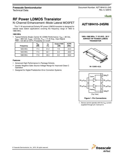
<strong>RF</strong> <strong>Power</strong> <strong>LDMOS</strong> <strong>Transistor</strong><br />
N--Channel Enhancement--Mode Lateral MOSFET<br />
This 71 W asymmetrical Doherty <strong>RF</strong> power <strong>LDMOS</strong> transistor is designed for<br />
cellular base station applications covering the frequency range of 1805 to<br />
1880 MHz.<br />
1800 MHz<br />
Typical Doherty Single--Carrier W--CDMA Performance: V DD =28Vdc,<br />
I DQA = 800 mA, V GSB =0.8Vdc,P out = 71 W Avg., Input Signal<br />
PAR = 9.9 dB @ 0.01% Probability on CCDF.<br />
A2T18H410 -24SR6<br />
1805–1880 MHz, 71 W AVG., 28 V<br />
AI<strong>RF</strong>AST <strong>RF</strong> POWER <strong>LDMOS</strong><br />
TRANSISTOR<br />
Frequency<br />
G ps<br />
(dB)<br />
D<br />
(%)<br />
Output PAR<br />
(dB)<br />
ACPR<br />
(dBc)<br />
1805 MHz 17.4 51.2 7.9 –34.5<br />
1840 MHz 17.5 50.1 8.3 –36.9<br />
1880 MHz 17.6 49.3 8.0 –36.8<br />
Features<br />
<br />
<br />
<br />
Advanced High Performance In--Package Doherty<br />
Greater Negative Gate--Source Voltage Range for Improved Class C<br />
Operation<br />
Designed for Digital Predistortion Error Correction Systems<br />
NI -1230S -4L2L<br />
VBW (1) A<br />
Carrier<br />
6<br />
<strong>RF</strong> inB /V GSB 2 4 <strong>RF</strong> outB /V DSB<br />
<strong>RF</strong> inA /V GSA 1 5 <strong>RF</strong> outA /V DSA<br />
Peaking<br />
(Top View)<br />
3<br />
VBW B<br />
(1)<br />
Figure 1. Pin Connections<br />
1. Device cannot operate with the V DD current<br />
supplied through pin 3 and pin 6.<br />
Freescale Semiconductor, Inc., 2015. All rights reserved.<br />
<strong>RF</strong> Device Data<br />
Freescale Semiconductor, Inc.<br />
A2T18H410 -24SR6<br />
1
Table 1. Maximum Ratings<br />
Rating Symbol Value Unit<br />
Drain--Source Voltage V DSS –0.5, +65 Vdc<br />
Gate--Source Voltage V GS –6.0, +10 Vdc<br />
Operating Voltage V DD 32, +0 Vdc<br />
Storage Temperature Range T stg –65 to +150 C<br />
Case Operating Temperature Range T C –40 to +150 C<br />
Operating Junction Temperature Range (1,2) T J –40 to +225 C<br />
CW Operation @ T C =25C<br />
Derate above 25C<br />
Table 2. Thermal Characteristics<br />
CW 282<br />
1.5<br />
W<br />
W/C<br />
Characteristic Symbol Value (2,3) Unit<br />
Thermal Resistance, Junction to Case<br />
Case Temperature 72C, 71 W Avg., W--CDMA, 28 Vdc, I DQA = 800 mA, V GSB =0.8Vdc,<br />
1840 MHz<br />
Table 3. ESD Protection Characteristics<br />
Test Methodology<br />
Human Body Model (per JESD22--A114) 2<br />
Machine Model (per EIA/JESD22--A115)<br />
Charge Device Model (per JESD22--C101)<br />
R JC 0.24 C/W<br />
Table 4. Electrical Characteristics (T A =25C unless otherwise noted)<br />
Characteristic Symbol Min Typ Max Unit<br />
Off Characteristics (4)<br />
Zero Gate Voltage Drain Leakage Current<br />
(V DS =65Vdc,V GS =0Vdc)<br />
Class<br />
I DSS — — 10 Adc<br />
B<br />
IV<br />
Zero Gate Voltage Drain Leakage Current<br />
(V DS =32Vdc,V GS =0Vdc)<br />
Gate--Source Leakage Current<br />
(V GS =5Vdc,V DS =0Vdc)<br />
On Characteristics - Side A (Carrier)<br />
Gate Threshold Voltage<br />
(V DS =10Vdc,I D = 160 Adc)<br />
Gate Quiescent Voltage<br />
(V DD =28Vdc,I DA = 800 mAdc, Measured in Functional Test)<br />
Drain--Source On--Voltage<br />
(V GS =10Vdc,I D =1.6Adc)<br />
On Characteristics - Side B (Peaking)<br />
Gate Threshold Voltage<br />
(V DS =10Vdc,I D = 270 Adc)<br />
Drain--Source On--Voltage<br />
(V GS =10Vdc,I D =2.7Adc)<br />
I DSS — — 1 Adc<br />
I GSS — — 1 Adc<br />
V GS(th) 1.4 1.5 2.3 Vdc<br />
V GS(Q) 2.2 2.6 3.0 Vdc<br />
V DS(on) 0.1 0.15 0.3 Vdc<br />
V GS(th) 0.8 1.2 1.6 Vdc<br />
V DS(on) 0.1 0.15 0.3 Vdc<br />
1. Continuous use at maximum temperature will affect MTTF.<br />
2. MTTF calculator available at http://www.freescale.com/rf/calculators.<br />
3. Refer to AN1955, Thermal Measurement Methodology of <strong>RF</strong> <strong>Power</strong> Amplifiers. Go to http://www.freescale.com/rf and search for AN1955.<br />
4. Each side of device measured separately.<br />
(continued)<br />
A2T18H410 -24SR6<br />
2<br />
<strong>RF</strong> Device Data<br />
Freescale Semiconductor, Inc.
Table 4. Electrical Characteristics (T A =25C unless otherwise noted) (continued)<br />
Characteristic Symbol Min Typ Max Unit<br />
Functional Tests (1,2) (In Freescale Doherty Test Fixture, 50 ohm system) V DD =28Vdc,I DQA = 800 mA, V GSB =0.8Vdc,P out =71WAvg.,<br />
f = 1805 MHz, Single--Carrier W--CDMA, IQ Magnitude Clipping, Input Signal PAR = 9.9 dB @ 0.01% Probability on CCDF. ACPR measured in<br />
3.84 MHz Channel Bandwidth @ 5 MHzOffset.<br />
<strong>Power</strong> Gain G ps 16.5 17.4 19.5 dB<br />
Drain Efficiency D 47.0 51.2 — %<br />
Output Peak--to--Average Ratio @ 0.01% Probability on CCDF PAR 7.4 7.9 — dB<br />
Adjacent Channel <strong>Power</strong> Ratio ACPR — –34.5 –28.0 dBc<br />
Load Mismatch (2) (In Freescale Doherty Test Fixture, 50 ohm system) I DQA = 800 mA, V GSB = 0.8 Vdc, f = 1840 MHz<br />
VSWR 10:1 at 32 Vdc, 440 W CW (3) Output <strong>Power</strong><br />
No Device Degradation<br />
(3 dB Input Overdrive from 376 W CW (3) Rated <strong>Power</strong>)<br />
Typical Performance (2) (In Freescale Doherty Test Fixture, 50 ohm system) V DD =28Vdc,I DQA = 800 mA, V GSB =0.8Vdc,<br />
1805–1880 MHz Bandwidth<br />
P out @ 1 dB Compression Point, CW P1dB — 355 (3) — W<br />
P out @ 3 dB Compression Point (4) P3dB — 457 — W<br />
AM/PM<br />
(Maximum value measured at the P3dB compression point across<br />
the 1805–1880 MHz frequency range)<br />
— –12.4 — <br />
VBW Resonance Point<br />
(IMD Third Order Intermodulation Inflection Point)<br />
VBW res — 90 — MHz<br />
Gain Flatness in 75 MHz Bandwidth @ P out =71WAvg. G F — 0.1 — dB<br />
Gain Variation over Temperature<br />
(–30C to+85C)<br />
G — 0.0056 — dB/C<br />
Output <strong>Power</strong> Variation over Temperature<br />
P1dB — 0.0077 — dB/C<br />
(–30C to+85C) (3)<br />
Table 5. Ordering Information<br />
Device Tape and Reel Information Package<br />
A2T18H410--24SR6 R6 Suffix = 150 Units, 56 mm Tape Width, 13--inch Reel NI--1230S--4L2L<br />
1. Part internally matched both on input and output.<br />
2. Measurements made with device in an asymmetrical Doherty configuration.<br />
3. Exceeds recommended operating conditions. See CW operation data in Maximum Ratings table.<br />
4. P3dB = P avg + 7.0 dB where P avg is the average output power measured using an unclipped W--CDMA single--carrier input signal where<br />
output PAR is compressed to 7.0 dB @ 0.01% probability on CCDF.<br />
<strong>RF</strong> Device Data<br />
Freescale Semiconductor, Inc.<br />
A2T18H410 -24SR6<br />
3
R1<br />
Z1<br />
C1<br />
D68602<br />
A2T18H410<br />
Rev. 4<br />
C7<br />
V DDA<br />
C3<br />
C5<br />
V GGB<br />
C2<br />
C8<br />
R2<br />
C4<br />
C6<br />
R3<br />
CUT OUT AREA<br />
C9<br />
C14<br />
C10<br />
C11<br />
C12<br />
C13<br />
C19<br />
C15<br />
C16<br />
C17<br />
C18<br />
V DDB V DDA<br />
Figure 2. A2T18H410 -24SR6 Test Circuit Component Layout<br />
Table 6. A2T18H410 -24SR6 Test Circuit Component Designations and Values<br />
Part Description Part Number Manufacturer<br />
C1, C7, C9, C14, C16, C19 10 uF Chip Capacitors C5750X7S2A106M230KB TDK<br />
C2, C8, C10, C15 12 pF Chip Capacitors ATC100B120JT500XT ATC<br />
C3 1.2 pF Chip Capacitor ATC100B1R2BT500XT ATC<br />
C4, C6 6.2 pF Chip Capacitors ATC100B6R2BT500XT ATC<br />
C5, C11 1.0 pF Chip Capacitors ATC100B1R0CT500XT ATC<br />
C12 5.1 pF Chip Capacitor ATC100B5R1CT500XT ATC<br />
C13 4.7 pF Chip Capacitor ATC100B4R7CT500XT ATC<br />
C17, C18 470 uF, 63 V Electrolytic Capacitors MCGPR63V477M13X26 Multicomp<br />
R1 50 Termination CW12010T0050GBK ATC<br />
R2, R3 2.7 , 1/4 W Chip Resistors CRCW12062R7FKEA Vishay<br />
Z1 1700–2000 MHz Band, 5 dB Directional Coupler X3C19P1-05S Anaren<br />
PCB Rogers RO4350B, 0.020, r =3.66 D68602 MTL<br />
A2T18H410 -24SR6<br />
4<br />
<strong>RF</strong> Device Data<br />
Freescale Semiconductor, Inc.
TYPICAL CHARACTERISTICS<br />
17.8<br />
56<br />
V DD =28Vdc,P out =71W(Avg.),I DQA = 800 mA<br />
17.7<br />
V GSB = 0.8 Vdc, Single--Carrier W--CDMA, 3.84 MHz 54<br />
17.6<br />
Channel Bandwidth, Input Signal PAR = 9.9 dB @<br />
52<br />
D<br />
0.01% Probability on CCDF<br />
17.5<br />
50<br />
17.4<br />
G ps<br />
48<br />
17.3<br />
17.2<br />
17.1<br />
17<br />
PARC<br />
–27<br />
–30<br />
–33<br />
–36<br />
–1.4<br />
–1.6<br />
–1.8<br />
–2<br />
16.9<br />
ACPR<br />
–39 –2.2<br />
16.8<br />
–42 –2.4<br />
1760 1780 1800 1820 1840 1860 1880 1900 1920<br />
f, FREQUENCY (MHz)<br />
Figure 3. Single -Carrier Output Peak -to -Average Ratio Compression<br />
(PARC) Broadband Performance @ P out = 71 Watts Avg.<br />
G ps , POWER GAIN (dB)<br />
D , DRAIN<br />
EFFICIENCY (%)<br />
ACPR (dBc)<br />
PARC (dB)<br />
IMD, INTERMODULATION DISTORTION (dBc)<br />
–10<br />
–20<br />
–30<br />
–40<br />
–50<br />
–60<br />
V DD =28Vdc,P out = 8 W (PEP), I DQA = 800 mA<br />
V GSB = 0.8 Vdc, Two--Tone Measurements<br />
(f1 + f2)/2 = Center Frequency of 1840 MHz<br />
IM3--U<br />
IM5--U<br />
IM7--L<br />
IM3--L<br />
IM5--L<br />
IM7--U<br />
–70<br />
1 10<br />
100<br />
500<br />
TWO--TONE SPACING (MHz)<br />
Figure 4. Intermodulation Distortion Products<br />
versus Two -Tone Spacing<br />
G ps , POWER GAIN (dB)<br />
17.8<br />
17.6<br />
17.4<br />
17.2<br />
17<br />
16.8<br />
OUTPUT COMPRESSION AT 0.01%<br />
PROBABILITY ON CCDF (dB)<br />
1<br />
0<br />
–1<br />
–2<br />
–3<br />
–4<br />
–1 dB = 55 W<br />
D<br />
ACPR<br />
V DD =28Vdc,I DQA = 800 mA, V GSB =0.8Vdc<br />
f = 1840 MHz, Single--Carrier W--CDMA<br />
3.84 MHz Channel Bandwidth<br />
–2 dB = 78.1 W<br />
–3 dB = 100 W<br />
PARC<br />
G ps<br />
60<br />
55<br />
50<br />
45<br />
40<br />
35<br />
D DRAIN EFFICIENCY (%)<br />
–30<br />
–32<br />
–34<br />
–36<br />
–38<br />
–40<br />
ACPR (dBc)<br />
16.6<br />
Input Signal PAR = 9.9 dB @ 0.01% Probability on CCDF<br />
–5<br />
30<br />
25 50 75 100 125 150<br />
P out , OUTPUT POWER (WATTS)<br />
Figure 5. Output Peak -to -Average Ratio<br />
Compression (PARC) versus Output <strong>Power</strong><br />
–42<br />
<strong>RF</strong> Device Data<br />
Freescale Semiconductor, Inc.<br />
A2T18H410 -24SR6<br />
5
TYPICAL CHARACTERISTICS<br />
G ps , POWER GAIN (dB)<br />
22<br />
20<br />
18<br />
16<br />
V DD =28Vdc,I DQA = 800 mA, V GSB =0.8Vdc<br />
Single--Carrier W--CDMA<br />
1805 MHz<br />
G ps<br />
1880 MHz<br />
1840 MHz<br />
1805 MHz<br />
1840 MHz<br />
1805 MHz<br />
1880 MHz<br />
14<br />
20<br />
1880 MHz<br />
1840 MHz<br />
12<br />
10<br />
3.84 MHz Channel Bandwidth, Input Signal<br />
10<br />
PAR = 9.9 dB @ 0.01% Probability on CCDF<br />
0<br />
1<br />
10 100 500<br />
P out , OUTPUT POWER (WATTS) AVG.<br />
Figure 6. Single -Carrier W -CDMA <strong>Power</strong> Gain, Drain<br />
Efficiency and ACPR versus Output <strong>Power</strong><br />
D<br />
ACPR<br />
60<br />
50<br />
40<br />
30<br />
D , DRAIN EFFICIENCY (%)<br />
0<br />
–10<br />
–20<br />
–30<br />
–40<br />
–50<br />
–60<br />
ACPR (dBc)<br />
22<br />
20<br />
18<br />
Gain<br />
GAIN (dB)<br />
16<br />
14<br />
12<br />
V DD =28Vdc<br />
P in =0dBm<br />
I DQA = 800 mA<br />
V GSB =0.8Vdc<br />
10<br />
1600 1680 1760 1840 1920 2000 2080 2160 2240<br />
f, FREQUENCY (MHz)<br />
Figure 7. Broadband Frequency Response<br />
A2T18H410 -24SR6<br />
6<br />
<strong>RF</strong> Device Data<br />
Freescale Semiconductor, Inc.
Table 7. Carrier Side Load Pull Performance — Maximum <strong>Power</strong> Tuning<br />
V DD =28Vdc,I DQA = 785 mA, Pulsed CW, 10 sec(on), 10% Duty Cycle<br />
f<br />
(MHz)<br />
Z source<br />
()<br />
Z in<br />
()<br />
Max Output <strong>Power</strong><br />
P1dB<br />
Z (1) load<br />
() Gain (dB) (dBm) (W)<br />
1805 1.32 – j3.98 1.36 + j3.59 1.01 – j3.41 18.7 52.6 181 58.4 –12<br />
1840 1.57 – j4.28 1.50 + j3.86 0.98 – j3.56 18.7 52.6 183 58.3 –12<br />
1880 2.23 – j4.77 1.99 + j4.16 0.98 – j3.75 18.6 52.6 181 57.2 –12<br />
D<br />
(%)<br />
AM/PM<br />
()<br />
f<br />
(MHz)<br />
Z source<br />
()<br />
Z in<br />
()<br />
Max Output <strong>Power</strong><br />
P3dB<br />
Z (2) load<br />
() Gain (dB) (dBm) (W)<br />
1805 1.32 – j3.98 1.22 + j3.74 1.02 – j3.56 16.5 53.3 215 59.4 –15<br />
1840 1.57 – j4.28 1.37 + j4.04 0.99 – j3.72 16.5 53.4 217 59.2 –15<br />
1880 2.23 – j4.77 1.87 + j4.43 1.00 – j3.90 16.4 53.3 214 58.3 –16<br />
(1) Load impedance for optimum P1dB power.<br />
(2) Load impedance for optimum P3dB power.<br />
Z source = Measured impedance presented to the input of the device at the package reference plane.<br />
Z in = Impedance as measured from gate contact to ground.<br />
Z load = Measured impedance presented to the output of the device at the package reference plane.<br />
Table 8. Carrier Side Load Pull Performance — Maximum Drain Efficiency Tuning<br />
V DD =28Vdc,I DQA = 785 mA, Pulsed CW, 10 sec(on), 10% Duty Cycle<br />
f<br />
(MHz)<br />
Z source<br />
()<br />
Z in<br />
()<br />
Max Drain Efficiency<br />
P1dB<br />
Z (1) load<br />
() Gain (dB) (dBm) (W)<br />
1805 1.32 – j3.98 1.35 + j3.89 2.22 – j2.08 22.4 49.9 98 72.1 –19<br />
1840 1.57 – j4.28 1.55 + j4.11 2.07 – j2.49 22.0 50.3 108 71.1 –17<br />
1880 2.23 – j4.77 2.11 + j4.44 1.93 – j2.67 21.8 50.4 109 70.0 –18<br />
D<br />
(%)<br />
D<br />
(%)<br />
AM/PM<br />
()<br />
AM/PM<br />
()<br />
f<br />
(MHz)<br />
Z source<br />
()<br />
Z in<br />
()<br />
Max Drain Efficiency<br />
P3dB<br />
Z (2) load<br />
() Gain (dB) (dBm) (W)<br />
1805 1.32 – j3.98 1.20 + j3.91 2.04 – j2.31 20.1 51.1 128 73.3 –25<br />
1840 1.57 – j4.28 1.38 + j4.21 1.96 – j2.52 19.9 51.2 130 72.5 –24<br />
1880 2.23 – j4.77 1.94 + j4.64 1.93 – j2.64 19.9 51.0 127 71.4 –24<br />
(1) Load impedance for optimum P1dB efficiency.<br />
(2) Load impedance for optimum P3dB efficiency.<br />
Z source = Measured impedance presented to the input of the device at the package reference plane.<br />
Z in = Impedance as measured from gate contact to ground.<br />
Z load = Measured impedance presented to the output of the device at the package reference plane.<br />
D<br />
(%)<br />
AM/PM<br />
()<br />
Input Load Pull<br />
Tuner and Test<br />
Circuit<br />
Output Load Pull<br />
Z load<br />
Device<br />
Z source Z in<br />
Under<br />
Test<br />
Tuner and Test<br />
Circuit<br />
<strong>RF</strong> Device Data<br />
Freescale Semiconductor, Inc.<br />
A2T18H410 -24SR6<br />
7
Table 9. Peaking Side Load Pull Performance — Maximum <strong>Power</strong> Tuning<br />
V DD =28Vdc,V GSB =0.8mA, Pulsed CW, 10 sec(on), 10% Duty Cycle<br />
f<br />
(MHz)<br />
Z source<br />
()<br />
Z in<br />
()<br />
Max Output <strong>Power</strong><br />
P1dB<br />
Z (1) load<br />
() Gain (dB) (dBm) (W)<br />
1805 1.32 – j3.98 1.55 + j4.16 1.38 – j3.61 15.9 54.9 312 57.4 –33<br />
1840 1.84 – j4.30 1.90 + j4.53 1.22 – j3.80 15.6 55.1 321 54.6 –32<br />
1880 2.67 – j4.46 2.83 + j4.90 1.40 – j3.92 16.0 55.0 315 56.4 –33<br />
D<br />
(%)<br />
AM/PM<br />
()<br />
f<br />
(MHz)<br />
Z source<br />
()<br />
Z in<br />
()<br />
Max Output <strong>Power</strong><br />
P3dB<br />
Z (2) load<br />
() Gain (dB) (dBm) (W)<br />
1805 1.32 – j3.98 1.59 + j4.36 1.35 – j3.73 13.7 55.7 370 59.3 –40<br />
1840 1.84 – j4.30 2.01 + j4.79 1.19 – j3.91 13.4 55.8 380 57.1 –39<br />
1880 2.67 – j4.46 3.20 + j5.21 1.38 – j4.21 13.6 55.7 372 57.3 –39<br />
(1) Load impedance for optimum P1dB power.<br />
(2) Load impedance for optimum P3dB power.<br />
Z source = Measured impedance presented to the input of the device at the package reference plane.<br />
Z in = Impedance as measured from gate contact to ground.<br />
Z load = Measured impedance presented to the output of the device at the package reference plane.<br />
Table 10. Peaking Side Load Pull Performance — Maximum Drain Efficiency Tuning<br />
V DD =28Vdc,V GSB =0.8mA, Pulsed CW, 10 sec(on), 10% Duty Cycle<br />
f<br />
(MHz)<br />
Z source<br />
()<br />
Z in<br />
()<br />
Max Drain Efficiency<br />
P1dB<br />
Z (1) load<br />
() Gain (dB) (dBm) (W)<br />
1805 1.32 – j3.98 1.39 + j4.15 3.59 – j2.93 17.2 53.0 201 69.3 –41<br />
1840 1.84 – j4.30 1.67 + j4.51 3.49 – j2.75 17.2 53.1 204 69.4 –40<br />
1880 2.67 – j4.46 2.45 + j4.92 3.12 – j2.36 17.3 53.0 199 68.8 –41<br />
D<br />
(%)<br />
D<br />
(%)<br />
AM/PM<br />
()<br />
AM/PM<br />
()<br />
f<br />
(MHz)<br />
Z source<br />
()<br />
Z in<br />
()<br />
Max Drain Efficiency<br />
P3dB<br />
Z (2) load<br />
() Gain (dB) (dBm) (W)<br />
1805 1.32 – j3.98 1.52 + j4.38 3.30 – j3.71 14.8 53.9 248 66.3 –47<br />
1840 1.84 – j4.30 1.91 + j4.81 2.68 – j3.69 14.8 54.7 292 66.2 –45<br />
1880 2.67 – j4.46 2.96 + j5.27 2.97 – j3.26 15.0 54.3 269 66.9 –47<br />
(1) Load impedance for optimum P1dB efficiency.<br />
(2) Load impedance for optimum P3dB efficiency.<br />
Z source = Measured impedance presented to the input of the device at the package reference plane.<br />
Z in = Impedance as measured from gate contact to ground.<br />
Z load = Measured impedance presented to the output of the device at the package reference plane.<br />
D<br />
(%)<br />
AM/PM<br />
()<br />
Input Load Pull<br />
Tuner and Test<br />
Circuit<br />
Output Load Pull<br />
Z load<br />
Device<br />
Z source Z in<br />
Under<br />
Test<br />
Tuner and Test<br />
Circuit<br />
A2T18H410 -24SR6<br />
8<br />
<strong>RF</strong> Device Data<br />
Freescale Semiconductor, Inc.
P1dB - TYPICAL CARRIER SIDE LOAD PULL CONTOURS — 1840 MHz<br />
IMAGINARY ()<br />
–1<br />
–1.5<br />
–2<br />
49<br />
48.5<br />
–2.5<br />
E<br />
49.5<br />
–3<br />
50.5 50<br />
51.5 51<br />
–3.5<br />
P<br />
52.5 52<br />
–4<br />
–4.5<br />
–5<br />
0.5 1 1.5 2 2.5 3 3.5<br />
REAL ()<br />
Figure 8. P1dB Load Pull Output <strong>Power</strong> Contours (dBm)<br />
IMAGINARY ()<br />
–1<br />
–1.5<br />
–2<br />
–2.5<br />
E<br />
–3<br />
70<br />
68 66<br />
–3.5<br />
P<br />
64<br />
62<br />
–4<br />
60<br />
58<br />
–4.5<br />
56<br />
–5<br />
0.5 1 1.5 2 2.5 3 3.5<br />
REAL ()<br />
Figure 9. P1dB Load Pull Efficiency Contours (%)<br />
IMAGINARY ()<br />
–1<br />
–1.5<br />
23<br />
–2<br />
22.5<br />
–2.5<br />
E<br />
22<br />
–3<br />
21.5<br />
–3.5<br />
P<br />
21<br />
20.5<br />
–4<br />
19.5 20<br />
–4.5<br />
19<br />
–5<br />
0.5 1 1.5 2 2.5 3 3.5<br />
REAL ()<br />
Figure 10. P1dB Load Pull Gain Contours (dB)<br />
IMAGINARY ()<br />
–1<br />
--10<br />
–10<br />
–1.5<br />
–22 –16<br />
–2<br />
–24 –20 –14<br />
–2.5<br />
E<br />
–12<br />
–18<br />
–3<br />
–3.5<br />
P<br />
–4<br />
–4.5<br />
–10<br />
–5<br />
–10<br />
0.5 1 1.5 2 2.5 3 3.5<br />
REAL ()<br />
Figure 11. P1dB Load Pull AM/PM Contours ()<br />
NOTE:<br />
P<br />
E<br />
= Maximum Output <strong>Power</strong><br />
= Maximum Drain Efficiency<br />
<strong>RF</strong> Device Data<br />
Freescale Semiconductor, Inc.<br />
A2T18H410 -24SR6<br />
9
P3dB - TYPICAL CARRIER SIDE LOAD PULL CONTOURS — 1840 MHz<br />
IMAGINARY ()<br />
–1<br />
–1.5<br />
–2<br />
50.5<br />
–2.5<br />
E<br />
51<br />
–3<br />
51.5<br />
–3.5<br />
P<br />
53 52.5 52<br />
–4<br />
49.5<br />
50<br />
–4.5<br />
–5<br />
0.5 1 1.5 2 2.5 3 3.5<br />
REAL ()<br />
Figure 12. P3dB Load Pull Output <strong>Power</strong> Contours (dBm)<br />
IMAGINARY ()<br />
–1<br />
–1.5<br />
–2<br />
72 70<br />
–2.5<br />
E<br />
68<br />
–3<br />
66<br />
–3.5<br />
P<br />
64<br />
–4<br />
62<br />
–4.5<br />
60<br />
56 58<br />
–5<br />
0.5 1 1.5 2 2.5 3 3.5<br />
REAL ()<br />
Figure 13. P3dB Load Pull Efficiency Contours (%)<br />
66<br />
–1<br />
–1.5<br />
–2<br />
20.5<br />
–1<br />
–1.5<br />
–2<br />
–30<br />
–28<br />
–20<br />
–26 –24 –22<br />
–18<br />
IMAGINARY ()<br />
–2.5<br />
–3<br />
–3.5<br />
–4<br />
–4.5<br />
P<br />
16.5<br />
17<br />
17.5<br />
E<br />
18.5<br />
18<br />
20<br />
19.5<br />
19<br />
IMAGINARY ()<br />
–2.5<br />
–3<br />
–3.5<br />
–4<br />
–4.5<br />
P<br />
E<br />
–14<br />
–16<br />
–5<br />
0.5 1 1.5 2 2.5 3 3.5<br />
REAL ()<br />
Figure 14. P3dB Load Pull Gain Contours (dB)<br />
–5<br />
0.5 1 1.5 2 2.5 3 3.5<br />
REAL ()<br />
Figure 15. P3dB Load Pull AM/PM Contours ()<br />
NOTE:<br />
P<br />
E<br />
= Maximum Output <strong>Power</strong><br />
= Maximum Drain Efficiency<br />
A2T18H410 -24SR6<br />
10<br />
<strong>RF</strong> Device Data<br />
Freescale Semiconductor, Inc.
P1dB – TYPICAL PEAKING LOAD PULL CONTOURS — 1840 MHz<br />
0<br />
–1<br />
51<br />
0<br />
–1<br />
62<br />
IMAGINARY ()<br />
51.5<br />
–2<br />
52<br />
E 52.5<br />
–3<br />
53<br />
P<br />
54.5 54 53.5<br />
–4<br />
55<br />
–5<br />
1 1.5 2 2.5 3 3.5 4 4.5 5 5.5 6<br />
REAL ()<br />
Figure 16. P1dB Load Pull Output <strong>Power</strong> Contours (dBm)<br />
IMAGINARY ()<br />
–2<br />
68<br />
E<br />
66<br />
–3<br />
64 62<br />
P<br />
–4<br />
60<br />
58<br />
54<br />
–5<br />
56 58<br />
56<br />
1 1.5 2 2.5 3 3.5 4 4.5 5 5.5 6<br />
REAL ()<br />
Figure 17. P1dB Load Pull Efficiency Contours (%)<br />
0<br />
0<br />
IMAGINARY ()<br />
–1<br />
–1<br />
18<br />
–28<br />
–44<br />
–2<br />
–2<br />
17.5<br />
17<br />
–42<br />
E<br />
–30<br />
E<br />
–3<br />
–3<br />
–40<br />
16.5<br />
P<br />
P<br />
–38<br />
–4<br />
–4<br />
15<br />
15.5<br />
16<br />
16<br />
–34<br />
–36<br />
–32<br />
–5<br />
–5<br />
1 1.5 2 2.5 3 3.5 4 4.5 5 5.5 6<br />
1 1.5 2 2.5 3 3.5 4 4.5 5 5.5 6<br />
REAL ()<br />
REAL ()<br />
Figure 18. P1dB Load Pull Gain Contours (dB)<br />
Figure 19. P1dB Load Pull AM/PM Contours ()<br />
IMAGINARY ()<br />
NOTE:<br />
P<br />
E<br />
= Maximum Output <strong>Power</strong><br />
= Maximum Drain Efficiency<br />
<strong>RF</strong> Device Data<br />
Freescale Semiconductor, Inc.<br />
A2T18H410 -24SR6<br />
11
P3dB - TYPICAL PEAKING SIDE LOAD PULL CONTOURS — 1840 MHz<br />
IMAGINARY ()<br />
–2<br />
52 52.5<br />
–2.5<br />
53.5 53 52.5 52<br />
–3<br />
–3.5<br />
P<br />
–4<br />
E<br />
54<br />
55.5 55<br />
–4.5<br />
54.5<br />
–5<br />
–5.5<br />
–6<br />
1 2 3 4 5 6 7<br />
REAL ()<br />
Figure 20. P3dB Load Pull Output <strong>Power</strong> Contours (dBm)<br />
IMAGINARY ()<br />
–2<br />
50<br />
–2.5<br />
–3<br />
66<br />
–3.5<br />
E<br />
P<br />
–4<br />
64 62<br />
60<br />
–4.5<br />
58<br />
–5<br />
–5.5<br />
56<br />
50 52 54<br />
52<br />
–6<br />
1 2 3 4 5 6 7<br />
REAL ()<br />
Figure 21. P3dB Load Pull Efficiency Contours (%)<br />
IMAGINARY ()<br />
–2<br />
–2<br />
15.5<br />
–50<br />
–2.5<br />
–2.5<br />
–3<br />
–3<br />
–50<br />
15<br />
–48<br />
–3.5<br />
–3.5<br />
E<br />
E<br />
P<br />
–4<br />
–4<br />
P<br />
–46<br />
14.5<br />
–44<br />
–4.5<br />
–4.5<br />
14<br />
–42<br />
–5<br />
–5<br />
12.5 13.5<br />
–36 –38 –40<br />
–5.5<br />
–5.5<br />
12 13<br />
–34<br />
–6<br />
–6<br />
1 2 3 4 5 6 7<br />
1 2 3 4 5 6 7<br />
REAL ()<br />
REAL ()<br />
IMAGINARY ()<br />
Figure 22. P3dB Load Pull Gain Contours (dB)<br />
Figure 23. P3dB Load Pull AM/PM Contours ()<br />
NOTE:<br />
P<br />
E<br />
= Maximum Output <strong>Power</strong><br />
= Maximum Drain Efficiency<br />
A2T18H410 -24SR6<br />
12<br />
<strong>RF</strong> Device Data<br />
Freescale Semiconductor, Inc.
PACKAGE DIMENSIONS<br />
<strong>RF</strong> Device Data<br />
Freescale Semiconductor, Inc.<br />
A2T18H410 -24SR6<br />
13
A2T18H410 -24SR6<br />
14<br />
<strong>RF</strong> Device Data<br />
Freescale Semiconductor, Inc.
PRODUCT DOCUMENTATION, SOFTWARE AND TOOLS<br />
Refer to the following resources to aid your design process.<br />
Application Notes<br />
AN1955: Thermal Measurement Methodology of <strong>RF</strong> <strong>Power</strong> Amplifiers<br />
Engineering Bulletins<br />
EB212: Using Data Sheet Impedances for <strong>RF</strong> <strong>LDMOS</strong> Devices<br />
Software<br />
Electromigration MTTF Calculator<br />
<strong>RF</strong> High <strong>Power</strong> Model<br />
.s2p File<br />
Development Tools<br />
Printed Circuit Boards<br />
To Download Resources Specific to a Given Part Number:<br />
1. Go to http://www.freescale.com/rf<br />
2. Search by part number<br />
3. Click part number link<br />
4. Choose the desired resource from the drop down menu<br />
The following table summarizes revisions to this document.<br />
REVISION HISTORY<br />
Revision Date Description<br />
0 May 2015 Initial Release of Data Sheet<br />
<strong>RF</strong> Device Data<br />
Freescale Semiconductor, Inc.<br />
A2T18H410 -24SR6<br />
15
How to Reach Us:<br />
Home Page:<br />
freescale.com<br />
Web Support:<br />
freescale.com/support<br />
Information in this document is provided solely to enable system and software<br />
implementers to use Freescale products. There are no express or implied copyright<br />
licenses granted hereunder to design or fabricate any integrated circuits based on the<br />
information in this document.<br />
Freescale reserves the right to make changes without further notice to any products<br />
herein. Freescale makes no warranty, representation, or guarantee regarding the<br />
suitability of its products for any particular purpose, nor does Freescale assume any<br />
liability arising out of the application or use of any product or circuit, and specifically<br />
disclaims any and all liability, including without limitation consequential or incidental<br />
damages. “Typical” parameters that may be provided in Freescale data sheets and/or<br />
specifications can and do vary in different applications, and actual performance may<br />
vary over time. All operating parameters, including “typicals,” must be validated for<br />
each customer application by customer’s technical experts. Freescale does not convey<br />
any license under its patent rights nor the rights of others. Freescale sells products<br />
pursuant to standard terms and conditions of sale, which can be found at the following<br />
address: freescale.com/SalesTermsandConditions.<br />
Freescale and the Freescale logo are trademarks of Freescale Semiconductor, Inc.,<br />
Reg. U.S. Pat. & Tm. Off. Airfast is a trademark of Freescale Semiconductor, Inc. All<br />
other product or service names are the property of their respective owners.<br />
E 2015 Freescale Semiconductor, Inc.<br />
A2T18H410 -24SR6<br />
Document Number: A2T18H410--24S<br />
16 Rev. 0, 5/2015<br />
<strong>RF</strong> Device Data<br />
Freescale Semiconductor, Inc.