RF Power LDMOS Transistor
1MmmaC4
1MmmaC4

Create successful ePaper yourself
Turn your PDF publications into a flip-book with our unique Google optimized e-Paper software.
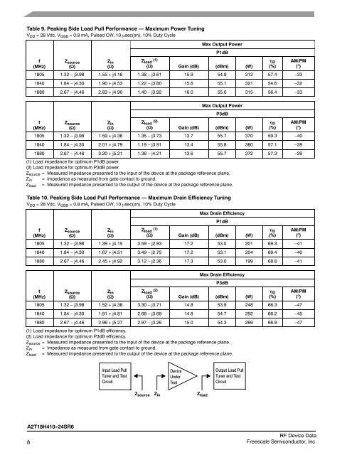
Table 9. Peaking Side Load Pull Performance — Maximum <strong>Power</strong> Tuning<br />
V DD =28Vdc,V GSB =0.8mA, Pulsed CW, 10 sec(on), 10% Duty Cycle<br />
f<br />
(MHz)<br />
Z source<br />
()<br />
Z in<br />
()<br />
Max Output <strong>Power</strong><br />
P1dB<br />
Z (1) load<br />
() Gain (dB) (dBm) (W)<br />
1805 1.32 – j3.98 1.55 + j4.16 1.38 – j3.61 15.9 54.9 312 57.4 –33<br />
1840 1.84 – j4.30 1.90 + j4.53 1.22 – j3.80 15.6 55.1 321 54.6 –32<br />
1880 2.67 – j4.46 2.83 + j4.90 1.40 – j3.92 16.0 55.0 315 56.4 –33<br />
D<br />
(%)<br />
AM/PM<br />
()<br />
f<br />
(MHz)<br />
Z source<br />
()<br />
Z in<br />
()<br />
Max Output <strong>Power</strong><br />
P3dB<br />
Z (2) load<br />
() Gain (dB) (dBm) (W)<br />
1805 1.32 – j3.98 1.59 + j4.36 1.35 – j3.73 13.7 55.7 370 59.3 –40<br />
1840 1.84 – j4.30 2.01 + j4.79 1.19 – j3.91 13.4 55.8 380 57.1 –39<br />
1880 2.67 – j4.46 3.20 + j5.21 1.38 – j4.21 13.6 55.7 372 57.3 –39<br />
(1) Load impedance for optimum P1dB power.<br />
(2) Load impedance for optimum P3dB power.<br />
Z source = Measured impedance presented to the input of the device at the package reference plane.<br />
Z in = Impedance as measured from gate contact to ground.<br />
Z load = Measured impedance presented to the output of the device at the package reference plane.<br />
Table 10. Peaking Side Load Pull Performance — Maximum Drain Efficiency Tuning<br />
V DD =28Vdc,V GSB =0.8mA, Pulsed CW, 10 sec(on), 10% Duty Cycle<br />
f<br />
(MHz)<br />
Z source<br />
()<br />
Z in<br />
()<br />
Max Drain Efficiency<br />
P1dB<br />
Z (1) load<br />
() Gain (dB) (dBm) (W)<br />
1805 1.32 – j3.98 1.39 + j4.15 3.59 – j2.93 17.2 53.0 201 69.3 –41<br />
1840 1.84 – j4.30 1.67 + j4.51 3.49 – j2.75 17.2 53.1 204 69.4 –40<br />
1880 2.67 – j4.46 2.45 + j4.92 3.12 – j2.36 17.3 53.0 199 68.8 –41<br />
D<br />
(%)<br />
D<br />
(%)<br />
AM/PM<br />
()<br />
AM/PM<br />
()<br />
f<br />
(MHz)<br />
Z source<br />
()<br />
Z in<br />
()<br />
Max Drain Efficiency<br />
P3dB<br />
Z (2) load<br />
() Gain (dB) (dBm) (W)<br />
1805 1.32 – j3.98 1.52 + j4.38 3.30 – j3.71 14.8 53.9 248 66.3 –47<br />
1840 1.84 – j4.30 1.91 + j4.81 2.68 – j3.69 14.8 54.7 292 66.2 –45<br />
1880 2.67 – j4.46 2.96 + j5.27 2.97 – j3.26 15.0 54.3 269 66.9 –47<br />
(1) Load impedance for optimum P1dB efficiency.<br />
(2) Load impedance for optimum P3dB efficiency.<br />
Z source = Measured impedance presented to the input of the device at the package reference plane.<br />
Z in = Impedance as measured from gate contact to ground.<br />
Z load = Measured impedance presented to the output of the device at the package reference plane.<br />
D<br />
(%)<br />
AM/PM<br />
()<br />
Input Load Pull<br />
Tuner and Test<br />
Circuit<br />
Output Load Pull<br />
Z load<br />
Device<br />
Z source Z in<br />
Under<br />
Test<br />
Tuner and Test<br />
Circuit<br />
A2T18H410 -24SR6<br />
8<br />
<strong>RF</strong> Device Data<br />
Freescale Semiconductor, Inc.