

EC6201_uw

Create successful ePaper yourself
Turn your PDF publications into a flip-book with our unique Google optimized e-Paper software.
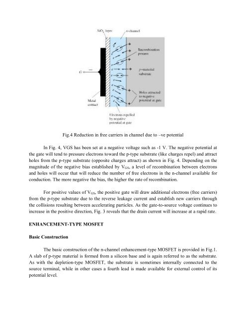
Fig.4 Reduction in free carriers in channel due to –ve potential<br />
In Fig. 4, VGS has been set at a negative voltage such as -1 V. The negative potential at<br />
the gate will tend to pressure electrons toward the p-type substrate (like charges repel) and attract<br />
holes from the p-type substrate (opposite charges attract) as shown in Fig. 4. Depending on the<br />
magnitude of the negative bias established by V GS , a level of recombination between electrons<br />
and holes will occur that will reduce the number of free electrons in the n-channel available for<br />
conduction. The more negative the bias, the higher the rate of recombination.<br />
For positive values of V GS , the positive gate will draw additional electrons (free carriers)<br />
from the p-type substrate due to the reverse leakage current and establish new carriers through<br />
the collisions resulting between accelerating particles. As the gate-to-source voltage continues to<br />
increase in the positive direction, Fig. 3 reveals that the drain current will increase at a rapid rate.<br />
ENHANCEMENT-TYPE MOSFET<br />
Basic Construction<br />
The basic construction of the n-channel enhancement-type MOSFET is provided in Fig.1.<br />
A slab of p-type material is formed from a silicon base and is again referred to as the substrate.<br />
As with the depletion-type MOSFET, the substrate is sometimes internally connected to the<br />
source terminal, while in other cases a fourth lead is made available for external control of its<br />
potential level.