

EC6201_uw

You also want an ePaper? Increase the reach of your titles
YUMPU automatically turns print PDFs into web optimized ePapers that Google loves.
Construction<br />
The diac can be constructed in either npn or pnp form.The two leads are connected to p regions<br />
of silicon separated by an n region. the structure of diac is similar to that of a transistor<br />
differences are<br />
There is no terminal attached to the base layer<br />
The three regions are nearly identical in size. the doping concentrations are<br />
identical to give the device symmetrical properties.<br />
Operation<br />
When a positive or negative voltage is applied across the terminals of Diac only a small leakage<br />
current Ibo will flow through the device as the applied voltage is increased , the leakage current<br />
will continue to flow until the voltage reaches breakover voltage Vbo at this point avalanche<br />
breakdown of the reverse biased junction occurs and the device exhibits negative resistance i.e<br />
current through the device increases with the decreasing values of applied voltage the voltage<br />
across the device then drops to breakback voltage Vw.<br />
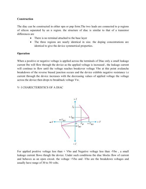
V- I CHARECTERISTICS OF A DIAC<br />
For applied positive voltage less than + Vbo and Negative voltage less than -Vbo , a small<br />
leakage current flows thrugh the device. Under such conditions the diac blocks flow of current<br />
and behaves as an open circuit. the voltage +Vbo and -Vbo are the breakdown voltages and<br />
usually have range of 30 to 50 volts.