TIMARIS - Singulus Technologies AG
TIMARIS - Singulus Technologies AG
TIMARIS - Singulus Technologies AG

You also want an ePaper? Increase the reach of your titles
YUMPU automatically turns print PDFs into web optimized ePapers that Google loves.
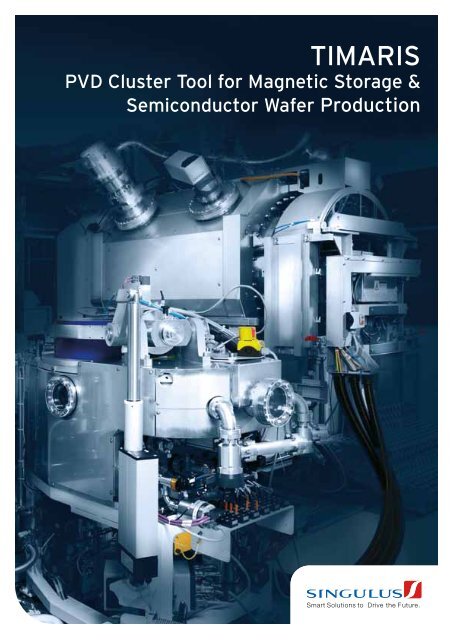
<strong>TIMARIS</strong><br />
PVD Cluster Tool for Magnetic Storage &<br />
Semiconductor Wafer Production<br />
Smart Solutions to Drive the F uture.
2<br />
<strong>TIMARIS</strong> – PVD Cluster Tool from SINGULUS<br />
SINGULUS TECHNOLOGIES<br />
(SINGULUS), founded in 1996,<br />
continues to expand its activities<br />
in the segments Semiconductor,<br />
Solar and Optical Disc.<br />
SINGULUS’ business unit Nano<br />
Deposition <strong>Technologies</strong> is a<br />
renowned manufacturer of advanced<br />
thin-film deposition equipment<br />
for MRAM and Thin-Film Head<br />
production. It is the trusted partner<br />
in the respective industry and<br />
extends its leadership in the<br />
thin-film deposition technology<br />
for Semiconductor applications.<br />
SINGULUS has already established<br />
and qualified the second generation<br />
of the <strong>TIMARIS</strong> PVD Cluster Tool<br />
platform in the market and is offering<br />
a complete portfolio of process<br />
modules for different applications.<br />
As today, seven different process<br />
modules are available to configure<br />
a <strong>TIMARIS</strong> system according to<br />
customer needs. These modules<br />
include the Multi-Target-Module<br />
(MTM), Oxidation-Process-Module<br />
(OPM), Pre-Clean-Module (PCM),<br />
Combi-Process-Module (CPM),<br />
Flexible-Target-Module (FTM) and<br />
Static-PVD-Module (sPVD-M) as<br />
well as the new Rotating-Substrate-<br />
Module (RSM).<br />
The <strong>TIMARIS</strong> PVD modules (MTM,<br />
FTM, RSM, sPVD-M) incorporate the<br />
full scope of sputtering techniques<br />
as: DC magnetron sputtering, pulsed<br />
DC magnetron sputtering and RF<br />
magnetron sputtering as well as<br />
combinations of these modes are<br />
selectable by recipe.
Multi Target Module<br />
Top: Target Drum with<br />
10 rectangular cathodes;<br />
Drum design ensures<br />
easy maintenance;<br />
Bottom: Main part of the<br />
chamber containing LDD<br />
equipment<br />
Oxidation Module<br />
Low Energy Remote<br />
Atomic Plasma Oxidation;<br />
Natural Oxidation;<br />
Soft Energy<br />
Surface Treatment<br />
Thin-Film Heads (TFH)<br />
_ High Moment Material<br />
(Writer Material)<br />
_ TMR (Reader Material)<br />
_ GMR (Reader Material)<br />
_ Deposition of seed and gap layers<br />
Semiconductor<br />
_ MRAM<br />
_ Sensors<br />
_ High-k dielectrics<br />
_ Metal gates<br />
_ Phase-change material deposition<br />
_ SAW/BAW film deposition<br />
_ In-circuit Inductors<br />
Ultra-High-Vacuum Design:<br />
High Throughput (e.g. MRAM):<br />
High Effective Up-time:<br />
Reliability:<br />
All <strong>TIMARIS</strong> applications require<br />
the deposition of ultra-thin metallic<br />
and insulating film stacks down to<br />
a thickness of one (1) nanometer<br />
and below with very precise material<br />
thickness and high uniformity<br />
specifications.<br />
The MTM is the key component<br />
of the <strong>TIMARIS</strong> platform; it<br />
incorporates the Linear Dynamic<br />
Deposition (LDD, US patent US<br />
7,799,179 B2) technology in<br />
combination with ten (10) sputter<br />
targets in one vacuum chamber.<br />
Base Pressure < 5*10-9 Torr<br />
(Deposition Chamber)<br />
up to 18 Wafer/h (see page 11)<br />
Maintenance friendly Design<br />
Solid and well Engineered Design,<br />
no fast moving Parts<br />
3<br />
Cassette Module<br />
(according to Customer<br />
Specification)<br />
Soft-Etch Module<br />
(PreClean, Surface<br />
Treatment)<br />
Transport Module<br />
(UHV wafer handler)<br />
The FTM module uses Linear<br />
Dynamic Deposition in combination<br />
with up to four cathodes. The LDD<br />
technology is especially designed<br />
for deposition of ultra-thin films,<br />
magnetic films, high-quality metallic,<br />
conductive and insulating films and is<br />
the key to deliver world class material<br />
uniformity across large wafer sizes,<br />
combined with an exceptional<br />
precise control of ultra-thin<br />
layer thickness down to 1 % of<br />
a nanometer.
4<br />
Linear Dynamic Deposition (LDD)<br />
Deposition Technique:<br />
Linear PVD Magnetron and<br />
linear movement of wafer<br />
Linear Dynamic Deposition (LDD)⋅<br />
_ Short target-substrate distance:<br />
_ Best coating efficiency<br />
_ Low cost of owner ship<br />
_ Thickness adjusted by wafer speed:<br />
_ Precise thickness control &<br />
repeatability<br />
_ Ultra thin film < 0.1 nm; smallest<br />
thickness step: < 0.01 nm<br />
_ Special LDD capabilities<br />
_ Deposition of thickness wedges<br />
_ Preparation of concentration<br />
gradients<br />
_ Multi-directional coating:<br />
_ Smooth films and interfaces<br />
_ Stationary Aligning Magnetic<br />
Field (AMF):<br />
_ Magnetic pre-alignment of easy<br />
axis direction<br />
_ Leakage field of cathode parallel<br />
to wafer travel direction:<br />
_ Ideal symmetry for magnetic<br />
film applications<br />
_ Robust and reliable design
Multi-Target-Module with<br />
10 DC/RF Cathodes<br />
Multiple film stack deposition, without<br />
the need to break ultra-high vacuum,<br />
is one of the key advantages of the<br />
MTM process module. Additional<br />
features as wafer heating for hot<br />
substrate deposition or a collinear<br />
Aligning Magnetic Field (AMF) can<br />
be activated to align the magnetic<br />
Easy Axis during deposition of<br />
ferromagnetic films.<br />
The Linear Dynamic Deposition (LDD)<br />
technology enables the capability to<br />
deposit wedge films with a different<br />
film thickness across the wafer and<br />
to deposit alloy films with adjustable<br />
concentration gradients across one<br />
wafer. Both features allow a very<br />
cost effective development of film<br />
stacks and accelerate the devices<br />
development.<br />
The LDD technology is the key to<br />
delivering world class material uniformity<br />
across large wafers and exceptional<br />
precise control of ultra thin layer<br />
thickness down to 1 %<br />
of a nanometer.<br />
Details:<br />
_ DC/RF magnetron<br />
_ All sputter deposition modes<br />
selectable by recipe for all<br />
10 cathodes<br />
_ LDD technology<br />
_ RF bias option<br />
_ Ultra-High-Vacuum technology,<br />
base pressure < 5*10 -9 Torr<br />
_ Wafer heating and cooling<br />
5<br />
Multi-Target-Module
6<br />
Flexible-Target-Module (FTM)<br />
Flexible-Target-Module with<br />
4 DC/RF Cathodes<br />
The Flexible-Target-Module (FTM)<br />
incorporates Linear Dynamic<br />
Deposition (LDD) technology in<br />
combination with up to four sputter<br />
targets in one vacuum chamber.<br />
The FTM incorporates the same<br />
functionalities like the Multi-Target-<br />
Module (MTM) as the substrate<br />
heating, the Aligning Magnetic Field<br />
and the capability to deposit wedge<br />
films with a different film thickness<br />
across the wafer and to deposit alloy<br />
films with adjustable concentration<br />
gradients across one wafer. The only<br />
difference of the FTM is the number<br />
of targets.<br />
Details:<br />
_ DC/RF magnetron<br />
_ All sputter deposition modes<br />
selectable by recipe for all<br />
4 cathodes<br />
_ LDD technology<br />
_ RF bias option<br />
_ Ultra-High-Vacuum technology,<br />
base pressure < 5*10 -9 Torr<br />
_ Wafer heating and cooling
Rotating-Substrate-Module<br />
(RSM)<br />
The Rotating-Substrate-Module<br />
(RSM) is a dedicated PVD module<br />
for R&D for different Semiconductors<br />
and other applications.<br />
Rotating-Substrate-Module (RSM)<br />
Essential technical features are:<br />
_ Up to 12 PVD cathodes in one<br />
chamber<br />
_ Rotating substrate deposition<br />
_ Co-sputtering<br />
_ DC-, pulsed DC-, RF-sputtering<br />
_ Wafer heating<br />
_ Base pressure < 10 -8 Torr<br />
_ In-situ aligning magnetic field<br />
_ Alternative equipment<br />
_ Ion source<br />
_ Surface metrology<br />
_ Low R&D costs<br />
7
8<br />
Pre-Clean-Module PCM)<br />
Pre-Clean-Module<br />
The Pre-Clean-Module (PCM) is used<br />
to clean the wafer prior to deposition.<br />
This is a standard technique employing<br />
sputter etch technology by applying<br />
RF power to the wafer. Typically the<br />
process removes residual water<br />
and other molecules and native<br />
oxides by adjusting the etching<br />
process parameters. Optionally,<br />
this module can also be equipped<br />
with an ECWR plasma source.<br />
This additional plasma source<br />
provides a more flexible etching<br />
process (higher etch rates, lower<br />
etching energies). The module<br />
geometry (large plasma source,<br />
rotational symmetric pump system)<br />
ensures a high uniformity of<br />
the etching.<br />
Details:<br />
_ Wafer cleaning, removal of native<br />
oxides by sputter etch<br />
_ ECWR plasma source as option<br />
_ Variable distance between and<br />
ion source<br />
_ Ultra-High-Vacuum technology,<br />
base pressure < 1*10 -8 Torr
Oxidation-Process-Module<br />
The Oxidation-Process-Module<br />
(OPM) is required to oxidize ultra-thin<br />
metallic films into insulating films of<br />
very high quality. Such films are<br />
required in Tunnel Magneto Resistance<br />
layer stacks as tunneling barriers.<br />
The barrier material of choice is<br />
nowadays MgO, but Al 2 O 3 and other<br />
materials have been considered.<br />
The oxidation can be performed by<br />
using a remote plasma provided by<br />
a ECWR plasma source. This source<br />
generates oxygen ions and radicals<br />
of very low adjustable energy.<br />
Alternatively, the oxidation can be<br />
performed by the so-called natural<br />
oxidation by exposing the metal film<br />
Oxidation-Process-Module (OPM)<br />
to pure oxygen of low pressure<br />
(10 Torr down to 0.1 m Torr). The<br />
module geometry (large plasma<br />
source, rotational symmetric pump<br />
system) ensures a high uniformity<br />
of the oxidation. Other applications<br />
for the OM are surface treatment<br />
of wafers by different activated<br />
gases (e.g. N 2 ).<br />
Details:<br />
_ Low energy remote plasma<br />
oxidation<br />
_ Natural oxidation<br />
_ Surface treatment by low<br />
energetic ions<br />
_ Variable distance between<br />
substrate and ion source<br />
_ Ultra-High-Vacuum technology,<br />
base pressure < 1*10 -8 Torr<br />
9
10<br />
Static-PVD-Module (sPVD-M)<br />
Static-PVD-Module<br />
The Static-PVD-Module (sPVD-M)<br />
comprises a standard magnetron<br />
cathode with optimized target<br />
utilization for high rate sputter<br />
deposition of metallic and nonconducting<br />
materials for multiple<br />
applications. DC magnetron as well<br />
as RF magnetron sputter modes are<br />
selectable through a recipe menu.<br />
The module is envisaged to be used<br />
for deposition of films with high<br />
deposition rate that do not require<br />
the extremely high uniformity that can<br />
be achieved by the LDD technology.<br />
Details:<br />
_ DC and RF sputter deposition<br />
selectable by recipe<br />
_ Variable distance between<br />
substrate and sputter target<br />
_ Ultra-High-Vacuum technology,<br />
base pressure < 1*10 -8 Torr
Combination-Process-Module<br />
The Combination-Process-Module<br />
(CPM) comprises both technologies,<br />
of oxidation and pre-clean in one<br />
module. This is a cost-efficient<br />
option, since only one module for<br />
two process steps is required. It is<br />
mainly envisaged for R&D purposes,<br />
where a high throughput is of less<br />
importance. The process performance<br />
is identical with the Oxidation-<br />
Module and the Pre-Clean-Module.<br />
Combi-Process-Module (CPM)<br />
Details:<br />
_ Low energy remote plasma<br />
oxidation<br />
_ Natural oxidation<br />
_ Surface treatment by low<br />
energetic ions<br />
_ Wafer cleaning, removal of native<br />
oxides by sputter etch<br />
_ Variable distance between<br />
substrate and ion source<br />
_ Ultra-High-Vacuum technology,<br />
base pressure < 1*10 -8 Torr<br />
11
Typical <strong>TIMARIS</strong> configuration<br />
for 300 mm MRAM wafer<br />
production with full throughput,<br />
consisting of:<br />
_ 2 Multi-Target-Modules<br />
_ 1 Oxidation-Module<br />
_ 1 Pre-Clean-Module<br />
_ 1 Transport Module (Brooks)<br />
including two FOUP Loadports<br />
_ Multiple wafer handling<br />
_ Throughput: up to 20 Wafer*<br />
_ Software integration:<br />
GEM/SECSII Interface<br />
* standard MRAM layer stack<br />
Typical <strong>TIMARIS</strong> configuration<br />
for 150/200 mm Thin-Film<br />
Head wafer production. The<br />
footprint shown is for a tool for<br />
TMR (GMR) sensor fabrication<br />
and consists of:<br />
_ 1 Multi-Target-Module<br />
_ 1 Oxidation-Module<br />
_ 1 Pre-Clean Module<br />
_ 1 Transport Module (Brooks)<br />
_ Multiple wafer handling<br />
_ Throughput: 9 wafers for a standard<br />
TMR layer stack<br />
_ Software integration:<br />
GEM/SECSII Interface<br />
_ Variants: HMM film deposition<br />
(no oxidation module)<br />
300 mm<br />
Wafer<br />
150 mm<br />
200 mm<br />
Wafer
<strong>TIMARIS</strong> configuration<br />
for 300 mm MRAM and<br />
semiconductor wafer<br />
production, consisting of:<br />
_ 1 Multi-Target-Module<br />
_ 3 Flexible-Target-Modules<br />
_ 1 Pre-Clean-Module<br />
_ 1 Oxidation-Module<br />
_ 1 Transport Module (Brooks)<br />
including three FOUP Loadports<br />
_ Multiple wafer handling<br />
_ Software integration:<br />
GEM/SECSII Interface<br />
Typical <strong>TIMARIS</strong> configuration<br />
for R&D purposes and/or low<br />
volume production. All wafer<br />
up to 300 mm wafer can be<br />
handled. The footprint shown<br />
consists of:<br />
_ 2 Rotating-Substrate-Modules<br />
_ 1 Combi-Process-Module<br />
_ 1 Transport Module<br />
all Wafer<br />
up to<br />
300 mm<br />
all Wafer<br />
up to<br />
300 mm
15<br />
Worldwide Sales & Service Network<br />
SINGULUS Serves Customers Worldwide<br />
SINGULUS Headquarters, Kahl/Main SINGULUS STANGL SOLAR, Fürstenfeldbruck<br />
SINGULUS Headquarters<br />
SINGULUS STANGL SOLAR<br />
Sales & Service Company<br />
Subsidiary
Headquarters<br />
SINGULUS TECHNOLOGIES <strong>AG</strong><br />
Hanauer Landstrasse 103<br />
D-63796 Kahl, Germany<br />
Tel. +49 6188 440-0<br />
Fax +49 6188 440-110<br />
sales@singulus.de<br />
www.singulus.de<br />
Affiliated Companies<br />
China<br />
SINGULUS MANUFACTURING<br />
GUANGZHOU LTD.<br />
Tel. +86 20 34885010<br />
frank@singulus.com.cn<br />
France<br />
SINGULUS TECHNOLOGIES<br />
FRANCE S.A.R.L.<br />
Tel. +33 3 893111-29<br />
singulus@club-internet.fr<br />
Germany<br />
SINGULUS STANGL SOLAR GMBH<br />
Tel. +49 8141 3600-0<br />
stangl@singulus.de<br />
Great Britain<br />
SINGULUS TECHNOLOGIES UK Ltd.<br />
Tel. +44 1793 7842-00<br />
brian.walsh@singulusuk.com<br />
Italy<br />
SINGULUS TECHNOLOGIES ITALIA S.R.L.<br />
Tel. +39 071 79303-12<br />
info@singulus.it<br />
Latin America<br />
SINGULUS TECHNOLOGIES<br />
LATIN AMERICA LTDA.<br />
Tel. +55 1121 6524-10<br />
rodolfo.mignone@singulus.com.br<br />
Netherlands<br />
SINGULUS TECHNOLOGIES <strong>AG</strong><br />
Branch Office Eindhoven<br />
Tel. +31 40 7501-400<br />
mastering@singulus.de<br />
Singapore<br />
SINGULUS TECHNOLOGIES<br />
ASIA PACIFIC PTE LTD.<br />
Tel. +65 674 119-12<br />
sales@singulus.com.sg<br />
Spain<br />
SINGULUS TECHNOLOGIES IBERICA S.L.<br />
Tel. +34 936 7500-25<br />
singulus@singulusib.com<br />
Taiwan<br />
SINGULUS TECHNOLOGIES TAIWAN LTD.<br />
Tel. +886 2 274833-66<br />
sales@singulus.com.tw<br />
United States and Canada<br />
SINGULUS TECHNOLOGIES INC.<br />
Tel. +1 860 68380-00<br />
sales@singulus.com<br />
05/2012 - MetaCom Printed in Germany - Technical alterations reserved