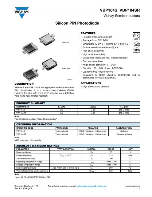
Silicon PIN Photodiode VBP104S, VBP104SR
Silicon PIN Photodiode VBP104S, VBP104SR
Silicon PIN Photodiode VBP104S, VBP104SR

You also want an ePaper? Increase the reach of your titles
YUMPU automatically turns print PDFs into web optimized ePapers that Google loves.
DESCRIPTION<br />
<strong>VBP104S</strong> and <strong>VBP104S</strong>R are high speed and high sensitive<br />
<strong>PIN</strong> photodiodes. It is a surface mount device (SMD)<br />
including the chip with a 4.4 mm 2 sensitive area detecting<br />
visible and near infrared radiation.<br />
<strong>Silicon</strong> <strong>PIN</strong> <strong>Photodiode</strong><br />
<strong>VBP104S</strong>, <strong>VBP104S</strong>R<br />
Vishay Semiconductors<br />
FEATURES<br />
• Package type: surface mount<br />
Package form: GW, RGW<br />
Dimensions (L x W x H in mm): 6.4 x 3.9 x 1.2<br />
Radiant sensitive area (in mm2 ): 4.4<br />
High photo sensitivity<br />
High radiant sensitivity<br />
Suitable for visible and near infrared radiation<br />
Fast response times<br />
Angle of half sensitivity: ϕ = ± 65°<br />
Floor life: 168 h, MSL 3, acc. J-STD-020<br />
Lead (Pb)-free reflow soldering<br />
Compliant to RoHS directive 2002/95/EC and in<br />
accordance to WEEE 2002/96/EC<br />
APPLICATIONS<br />
High speed photo detector<br />
PRODUCT SUMMARY<br />
COMPONENT Ira (µA) ϕ (deg) λ0.1 (nm)<br />
<strong>VBP104S</strong> 35 ± 65 430 to 1100<br />
<strong>VBP104S</strong>R<br />
Note<br />
Test conditions see table “Basic Characteristics”<br />
35 ± 65 430 to 1100<br />
Note<br />
MOQ: minimum order quantity<br />
Note<br />
Tamb = 25 °C, unless otherwise specified<br />
<strong>VBP104S</strong><br />
<strong>VBP104S</strong>R<br />
21733-1<br />
ORDERING INFORMATION<br />
ORDERING CODE PACKAGING REMARKS PACKAGE FORM<br />
<strong>VBP104S</strong> Tape and reel MOQ: 1000 pcs, 1000 pcs/reel Gullwing<br />
<strong>VBP104S</strong>R Tape and reel MOQ: 1000 pcs, 1000 pcs/reel Reverse gullwing<br />
ABSOLUTE MAXIMUM RATINGS<br />
PARAMETER TEST CONDITION SYMBOL VALUE UNIT<br />
Reverse voltage VR 60 V<br />
Power dissipation Tamb ≤ 25 °C PV 215 mW<br />
Junction temperature Tj 100 °C<br />
Operating temperature range Tamb - 40 to + 100 °C<br />
Storage temperature range Tstg - 40 to + 100 °C<br />
Soldering temperature Acc. reflow solder profile fig. 8 Tsd 260 °C<br />
Thermal resistance junction/ambient RthJA 350 K/W<br />
Document Number: 81170 For technical questions, contact: detectortechsupport@vishay.com www.vishay.com<br />
Rev. 1.0, 13-Aug-09 1
<strong>VBP104S</strong>, <strong>VBP104S</strong>R<br />
Vishay Semiconductors<br />
BASIC CHARACTERISTICS<br />
Note<br />
Tamb = 25 °C, unless otherwise specified<br />
BASIC CHARACTERISTICS<br />
Tamb = 25 °C, unless otherwise specified<br />
<strong>Silicon</strong> <strong>PIN</strong> <strong>Photodiode</strong><br />
PARAMETER TEST CONDITION SYMBOL MIN. TYP. MAX. UNIT<br />
Forward voltage IF = 50 mA VF 1 1.3 V<br />
Breakdown voltage IR = 100 µA, E = 0 V(BR) 60 V<br />
Reverse dark current VR = 10 V, E = 0 Iro 2 30 nA<br />
Diode capacitance<br />
VR = 0 V, f = 1 MHz, E = 0<br />
VR = 3 V, f = 1 MHz, E = 0<br />
CD<br />
CD<br />
48<br />
17 40<br />
pF<br />
pF<br />
Open circuit voltage Ee = 1 mW/cm2 , λ = 950 nm Vo 350 mV<br />
Temperature coefficient of Vo Ee = 1 mW/cm2 , λ = 950 nm TKVo - 2.6 mV/K<br />
Short circuit current Ee = 1 mW/cm2 , λ = 950 nm Ik 32 µA<br />
Temperature coefficient of Ik Ee = 1 mW/cm2 , λ = 950 nm TKIk 0.1 %/K<br />
Reverse light current<br />
Ee = 1 mW/cm2 , λ = 950 nm,<br />
VR = 5 V<br />
Ira 25 35 µA<br />
Angle of half sensitivity ϕ ± 65 deg<br />
Wavelength of peak sensitivity λp 940 nm<br />
Range of spectral bandwidth λ0.1 430 to 1100 nm<br />
Noise equivalent power VR = 10 V, λ = 950 nm NEP 4 x 10-14 W/√Hz<br />
Rise time<br />
Fall time<br />
I ro - Reverse Dark Current (nA)<br />
1000<br />
100<br />
10<br />
V R = 10 V<br />
VR = 10 V, RL = 1 kΩ,<br />
λ = 820 nm<br />
VR = 10 V, RL = 1 kΩ,<br />
λ = 820 nm<br />
tr 100 ns<br />
tf 100 ns<br />
1<br />
0.6<br />
20 40 60 80 100<br />
0 20 40 60 80 100<br />
94 8403 Tamb - Ambient Temperature (°C)<br />
94 8409 T amb - Ambient Temperature (°C)<br />
Fig. 1 - Reverse Dark Current vs. Ambient Temperature Fig. 2 - Relative Reverse Light Current vs. Ambient Temperature<br />
www.vishay.com For technical questions, contact: detectortechsupport@vishay.com Document Number: 81170<br />
2 Rev. 1.0, 13-Aug-09<br />
I - Relative Reverse Light Current<br />
ra rel<br />
1.4<br />
1.2<br />
1.0<br />
0.8<br />
VR =5V<br />
λ = 950 nm
I ra - Reverse Light Current (µA)<br />
0.1<br />
0.01 0.1 1<br />
94 8421<br />
Ee - Irradiance (mW/cm ) 2<br />
I ra - Reverse Light Current (µA)<br />
C D - Diode Capacitance (pF)<br />
1000<br />
100<br />
10<br />
1<br />
100<br />
Fig. 3 - Reverse Light Current vs. Irradiance<br />
10<br />
94 8422<br />
1<br />
0.1 1 10<br />
VR =5V<br />
λ= 950 nm<br />
Fig. 4 - Reverse Light Current vs. Reverse Voltage<br />
80<br />
60<br />
40<br />
20<br />
94 8423<br />
λ = 950 nm<br />
1 mW/cm 2<br />
0.5 mW/cm 2<br />
0.2 mW/cm 2<br />
0.1 mW/cm 2<br />
0.05 mW/cm 2<br />
V R - Reverse Voltage (V)<br />
E = 0<br />
f = 1 MHz<br />
0<br />
0.1 1 10<br />
V R - Reverse Voltage (V)<br />
Fig. 5 - Diode Capacitance vs. Reverse Voltage<br />
10<br />
100<br />
100<br />
<strong>VBP104S</strong>, <strong>VBP104S</strong>R<br />
<strong>Silicon</strong> <strong>PIN</strong> <strong>Photodiode</strong> Vishay Semiconductors<br />
0<br />
350 550 750 950<br />
Fig. 6 - Relative Spectral Sensitivity vs. Wavelength<br />
Fig. 7 - Relative Radiant Sensitivity vs. Angular Displacement<br />
Document Number: 81170 For technical questions, contact: detectortechsupport@vishay.com www.vishay.com<br />
Rev. 1.0, 13-Aug-09 3<br />
S(λ) rel - Relative Spectral Sensitivity<br />
S rel - Relative Radiant Sensitivity<br />
1.0<br />
0.8<br />
0.6<br />
0.4<br />
0.2<br />
94 8420 λ - Wavelength (nm)<br />
1.0<br />
0.9<br />
0.8<br />
0.7<br />
94 8406<br />
0.6<br />
0°<br />
0.4 0.2 0<br />
10° 20°<br />
1150<br />
30°<br />
40°<br />
50°<br />
60°<br />
70°<br />
80°<br />
ϕ - Angular Displacement
<strong>VBP104S</strong>, <strong>VBP104S</strong>R<br />
Vishay Semiconductors<br />
<strong>Silicon</strong> <strong>PIN</strong> <strong>Photodiode</strong><br />
PACKAGE DIMENSIONS FOR <strong>VBP104S</strong> in millimeters<br />
PACKAGE DIMENSIONS FOR <strong>VBP104S</strong>R in millimeters<br />
www.vishay.com For technical questions, contact: detectortechsupport@vishay.com Document Number: 81170<br />
4 Rev. 1.0, 13-Aug-09<br />
21728<br />
21729
TA<strong>PIN</strong>G DIMENSIONS FOR <strong>VBP104S</strong> in millimeters<br />
TA<strong>PIN</strong>G DIMENSIONS FOR <strong>VBP104S</strong>R in millimeters<br />
21731<br />
21730<br />
<strong>VBP104S</strong>, <strong>VBP104S</strong>R<br />
<strong>Silicon</strong> <strong>PIN</strong> <strong>Photodiode</strong> Vishay Semiconductors<br />
Document Number: 81170 For technical questions, contact: detectortechsupport@vishay.com www.vishay.com<br />
Rev. 1.0, 13-Aug-09 5
<strong>VBP104S</strong>, <strong>VBP104S</strong>R<br />
Vishay Semiconductors<br />
<strong>Silicon</strong> <strong>PIN</strong> <strong>Photodiode</strong><br />
REEL DIMENSIONS FOR <strong>VBP104S</strong> AND <strong>VBP104S</strong>R in millimeters<br />
SOLDER PROFILE<br />
Temperature (°C)<br />
19841<br />
300<br />
250<br />
200<br />
150<br />
100<br />
50<br />
21732<br />
255 °C<br />
240 °C<br />
217 °C<br />
max. 120 s<br />
0<br />
0 50 100 150 200 250 300<br />
Time (s)<br />
max. 30 s<br />
max. 100 s<br />
max. 260 °C<br />
245 °C<br />
max. ramp up 3 °C/s max. ramp down 6 °C/s<br />
Fig. 8 - Lead (Pb)-free Reflow Solder Profile<br />
acc. J-STD-020<br />
DRYPACK<br />
Devices are packed in moisture barrier bags (MBB) to<br />
prevent the products from moisture absorption during<br />
transportation and storage. Each bag contains a desiccant.<br />
FLOOR LIFE<br />
Time between soldering and removing from MBB must not<br />
exceed the time indicated in J-STD-020:<br />
Moisture sensitivity: level 3<br />
Floor life: 168 h<br />
Conditions: Tamb < 30 °C, RH < 60 %<br />
DRYING<br />
In case of moisture absorption devices should be baked<br />
before soldering. Conditions see J-STD-020 or<br />
recommended conditions:<br />
192 h at 40 °C (+ 5 °C), RH < 5 %<br />
or<br />
96 h at 60 °C (+ 5 °C), RH < 5 %.<br />
www.vishay.com For technical questions, contact: detectortechsupport@vishay.com Document Number: 81170<br />
6 Rev. 1.0, 13-Aug-09
Disclaimer<br />
All product specifications and data are subject to change without notice.<br />
Legal Disclaimer Notice<br />
Vishay<br />
Vishay Intertechnology, Inc., its affiliates, agents, and employees, and all persons acting on its or their behalf<br />
(collectively, “Vishay”), disclaim any and all liability for any errors, inaccuracies or incompleteness contained herein<br />
or in any other disclosure relating to any product.<br />
Vishay disclaims any and all liability arising out of the use or application of any product described herein or of any<br />
information provided herein to the maximum extent permitted by law. The product specifications do not expand or<br />
otherwise modify Vishay’s terms and conditions of purchase, including but not limited to the warranty expressed<br />
therein, which apply to these products.<br />
No license, express or implied, by estoppel or otherwise, to any intellectual property rights is granted by this<br />
document or by any conduct of Vishay.<br />
The products shown herein are not designed for use in medical, life-saving, or life-sustaining applications unless<br />
otherwise expressly indicated. Customers using or selling Vishay products not expressly indicated for use in such<br />
applications do so entirely at their own risk and agree to fully indemnify Vishay for any damages arising or resulting<br />
from such use or sale. Please contact authorized Vishay personnel to obtain written terms and conditions regarding<br />
products designed for such applications.<br />
Product names and markings noted herein may be trademarks of their respective owners.<br />
Document Number: 91000 www.vishay.com<br />
Revision: 18-Jul-08 1