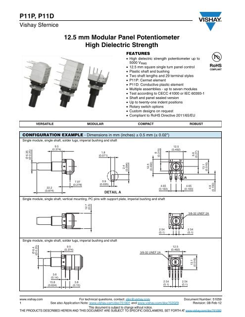
P11P, P11D 12.5 mm Modular Panel Potentiometer ... - TTI Europe
P11P, P11D 12.5 mm Modular Panel Potentiometer ... - TTI Europe
P11P, P11D 12.5 mm Modular Panel Potentiometer ... - TTI Europe

Create successful ePaper yourself
Turn your PDF publications into a flip-book with our unique Google optimized e-Paper software.
<strong>P11P</strong>, <strong>P11D</strong><br />
Vishay Sfernice<br />
<strong>12.5</strong> <strong>mm</strong> <strong>Modular</strong> <strong>Panel</strong> <strong>Potentiometer</strong><br />
High Dielectric Strength<br />
FEATURES<br />
� High dielectric strength potentiometer up to<br />
5000 VRMS<br />
� <strong>12.5</strong> <strong>mm</strong> square single turn panel control<br />
� Plastic shaft and bushing<br />
� Two shaft lengths and 29 terminal styles<br />
� <strong>P11P</strong>: Cermet element<br />
� <strong>P11D</strong>: Conductive plastic element<br />
� Multiple assemblies - up to seven modules<br />
� Test according to CECC 41000 or IEC 60393-1<br />
� Shaft and panel sealed version<br />
� Up to twenty-one indent positions<br />
� Rotary switch options<br />
� Custom designs on request<br />
� Compliant to RoHS Directive 2011/65/EU<br />
VERSATILE MODULAR COMPACT ROBUST<br />
CONFIGURATION EXAMPLE - Dimensions in <strong>mm</strong> (inches) ± 0.5 <strong>mm</strong> (± 0.02")<br />
Single module, single shaft, solder lugs, imperial bushing and shaft<br />
Ø 6.35<br />
(Ø 0.25)<br />
Single module, single shaft, vertical mounting, PC pins with support plate, imperial bushing and shaft<br />
Single module, single shaft, solder lugs, imperial bushing and shaft<br />
Ø 6.4<br />
(Ø 0.25)<br />
22.2<br />
(0.874)<br />
9.5<br />
(0.374)<br />
3.6<br />
(0.14)<br />
15.8<br />
(0.624)<br />
9.5<br />
(0.374)<br />
7.07<br />
(0.278)<br />
3.8<br />
(0.15)<br />
12.7<br />
(0.5)<br />
1.8<br />
(0.071)<br />
0.9<br />
(0.035)<br />
DETAIL A<br />
<strong>12.5</strong><br />
(0.492)<br />
www.vishay.com For technical questions, contact: sfer@vishay.com Document Number: 51059<br />
1 See also Application Note: www.vishay.com/doc?51001 and www.vishay.com/doc?52029<br />
This document is subject to change without notice.<br />
Revision: 08-Feb-12<br />
THE PRODUCTS DESCRIBED HEREIN AND THIS DOCUMENT ARE SUBJECT TO SPECIFIC DISCLAIMERS, SET FORTH AT www.vishay.com/doc?91000<br />
2.4<br />
(0.094)<br />
<strong>12.5</strong><br />
(0.492)<br />
8<br />
(0.315)<br />
3/8-32 UNEF 2A<br />
4.65<br />
(0.183)<br />
2.54<br />
(0.1)<br />
2.54<br />
(0.1)<br />
<strong>12.5</strong><br />
(0.492)<br />
A<br />
6.8<br />
(0.27)<br />
4.65<br />
(0.183)<br />
2.54<br />
(0.1)<br />
13.1<br />
(0.516)<br />
3/8-32 UNEF 2A<br />
2.54<br />
(0.1)<br />
13.1<br />
(0.516)<br />
4.9<br />
(0.193)
GENERAL SPECIFICATIONS<br />
ELECTRICAL (initial)<br />
Note<br />
(1) Consult Vishay Sfernice for other ohmic values<br />
<strong>12.5</strong> <strong>mm</strong> <strong>Modular</strong> <strong>Panel</strong> <strong>Potentiometer</strong><br />
High Dielectric Strength<br />
<strong>P11P</strong>, <strong>P11D</strong><br />
Vishay Sfernice<br />
<strong>P11D</strong> <strong>P11P</strong><br />
Resistive Element Conductive plastic Cermet<br />
Electrical Travel 270° ± 10° 270° ± 10°<br />
Resistance Range (1)<br />
Linear Taper<br />
Non-Linear Taper<br />
1 k� to 1 M�<br />
470 � to 500 k�<br />
20 � to 10 M�<br />
100 � to 2.2 M�<br />
Tolerance<br />
Taper<br />
Circuit Diagram<br />
Power Rating at 70 °C<br />
Standard ± 20 % ± 20 %<br />
On Request - ± 5 % or ± 10 %<br />
Linear Taper 0.5 W at + 70 °C 1 W at + 70 °C<br />
Non-Linear Taper 0.25 W at + 70 °C 0.5 W at + 70 °C<br />
Multiple Assemblies 0.25 W at + 70 °C per module 0.5 W at + 70 °C per module<br />
Temperature Coefficient, - 40 °C to + 100 °C (Typical) ± 500 ppm ± 150 ppm<br />
Limiting Element Voltage 350 V 350 V<br />
End Resistance (Typical) 2 � 2 �<br />
Contact Resistance Variation Linear Taper 1 % 2 % or 3 �<br />
Independent Linearity (Typical) Linear Taper ± 5 % ± 5 %<br />
Insulation Resistance 106 M� min. 106 M� min.<br />
Dielectric Strength<br />
Leads to Support Plate<br />
Leads to Shaft and Bushing<br />
3000 VRMS min.<br />
5000 VRMS min.<br />
3000 VRMS min.<br />
5000 VRMS min.<br />
Mechanical Endurance 50 000 cycles 50 000 cycles<br />
Document Number: 51059 For technical questions, contact: sfer@vishay.com www.vishay.com<br />
Revision: 08-Feb-12 See also Application Note: www.vishay.com/doc?51001 and www.vishay.com/doc?52029<br />
This document is subject to change without notice.<br />
2<br />
THE PRODUCTS DESCRIBED HEREIN AND THIS DOCUMENT ARE SUBJECT TO SPECIFIC DISCLAIMERS, SET FORTH AT www.vishay.com/doc?91000<br />
Rated Power (W)<br />
Vs %<br />
Ve<br />
1.25<br />
1<br />
0.75<br />
0.5<br />
0.25<br />
0<br />
0<br />
90 %<br />
50 %<br />
20 %<br />
10 %<br />
10<br />
20<br />
31°<br />
R<br />
A<br />
F S<br />
W<br />
50 %<br />
15° Electrical travel 270 °C<br />
a<br />
(1)<br />
<strong>P11P</strong> Linear Taper<br />
30<br />
L<br />
Electrical travel<br />
with switch 238°<br />
Mechanical travel 300 °C<br />
40<br />
b<br />
(2)<br />
<strong>P11P</strong> Non-Linear Taper<br />
<strong>P11D</strong> Linear Taper<br />
<strong>P11D</strong> Non-Linear Taper<br />
50<br />
60<br />
cw<br />
c<br />
(3)<br />
15°<br />
31°<br />
70 80 90 100 110 120 130<br />
Ambient Temperature (°C)
<strong>P11P</strong>, <strong>P11D</strong><br />
Vishay Sfernice<br />
MECHANICAL (initial)<br />
<strong>12.5</strong> <strong>mm</strong> <strong>Modular</strong> <strong>Panel</strong> <strong>Potentiometer</strong><br />
High Dielectric Strength<br />
Mechanical Travel<br />
Operating Torque (Typical)<br />
300° ± 5°<br />
Single and Dual Assemblies 0.2 Ncm to 1 Ncm max. (0.3 oz.-inch to 1.4 oz.-inch max.)<br />
Three to Seven Modules (Per Module) 0.2 Ncm to 0.3 Ncm max. (0.3 oz.-inch to 0.45 oz.-inch max.)<br />
End Stop Torque 80 Ncm max. (6.8 lb-inch max.)<br />
Tightening Torque<br />
Weight<br />
150 Ncm max. (13 lb-inch max.)<br />
Single Assemblies 3.5 g<br />
Two to Seven Modules (Per Module) 1.5 g to 2 g (0.25 oz. to 0.32 oz.)<br />
ENVIRONMENTAL<br />
<strong>P11D</strong> <strong>P11P</strong><br />
Operating Temperature Range - 40 °C to + 100 °C - 40 °C to + 100 °C<br />
Climatic Category 40/100/21 40/100/56<br />
Sealing IP64 IP64<br />
Storage Temperature - 40 °C to + 100 °C - 40 °C to + 100 °C<br />
MARKING<br />
� <strong>Potentiometer</strong> Module<br />
Vishay logo, nominal ohmic value (�, k�, M�), two stars<br />
identify <strong>P11D</strong> version, tolerance in % - variation law,<br />
manufacturing date (four digits), “3” for the lead 3<br />
� Switch Module<br />
Version, manufacturing date (four digits), “c” for co<strong>mm</strong>on lead<br />
� Indent Module<br />
Version, manufacturing date (four digits)<br />
PERFORMANCES<br />
TESTS CONDITIONS<br />
Electrical Endurance<br />
1000 h at rated power<br />
90’/30’ - ambient temp. 70 °C<br />
PACKAGING<br />
www.vishay.com For technical questions, contact: sfer@vishay.com Document Number: 51059<br />
3 See also Application Note: www.vishay.com/doc?51001 and www.vishay.com/doc?52029<br />
This document is subject to change without notice.<br />
Revision: 08-Feb-12<br />
THE PRODUCTS DESCRIBED HEREIN AND THIS DOCUMENT ARE SUBJECT TO SPECIFIC DISCLAIMERS, SET FORTH AT www.vishay.com/doc?91000<br />
� Box<br />
�RT/RT<br />
Contact resistance variation<br />
TYPICAL VALUE AND DRIFTS<br />
<strong>P11D</strong> <strong>P11P</strong><br />
± 10 %<br />
± 5 %<br />
± 2 %<br />
± 4 %<br />
Change of Temperature - 40 °C to + 100 °C, 5 cycles �RT/RT ± 0.5 % ± 0.2 %<br />
Damp Heat, Steady State<br />
+ 40 °C, 93 % relative humidity<br />
<strong>P11P</strong>: 56 days, <strong>P11D</strong>: 21 days<br />
Mechanical Endurance 50 000 cycles<br />
Climatic Sequence<br />
Shock<br />
Vibration<br />
Dry heat at + 125 °C/damp heat<br />
cold - 55 °C/damp heat, 5 cycles<br />
50 g’s, 11 ms<br />
3 shocks - 3 directions<br />
10 Hz to 55 Hz<br />
0.75 <strong>mm</strong> or 10 g’s, 6 h<br />
�RT/RT<br />
Insulation resistance<br />
�RT/RT<br />
Contact resistance variation<br />
± 5 %<br />
> 10 M�<br />
± 6 %<br />
± 4 %<br />
± 2 %<br />
> 1000 M�<br />
± 5 %<br />
± 5 %<br />
�RT/RT - ± 1 %<br />
�RT/RT<br />
�R1-2/R1-2<br />
�RT/RT<br />
�V1-2/V1-3<br />
± 0.2 %<br />
± 0.5 %<br />
± 0.2 %<br />
± 0.5 %<br />
± 0.2 %<br />
± 0.5 %<br />
± 0.2 %<br />
± 0.5 %
ORDERING INFORMATION (Part Number)<br />
MODEL STYLE<br />
P11 P =<br />
Cermet element<br />
D =<br />
Conductive plastic<br />
(audio)<br />
<strong>12.5</strong> <strong>mm</strong> <strong>Modular</strong> <strong>Panel</strong> <strong>Potentiometer</strong><br />
High Dielectric Strength<br />
NUMBER<br />
OF<br />
MODULES<br />
STANDARD RESISTANCE ELEMENT DATA<br />
STANDARD<br />
RESISTANCE<br />
VALUES<br />
1<br />
2<br />
3<br />
4<br />
5<br />
6<br />
7<br />
BUSHING OPTION SHAFT<br />
SHAFT<br />
STYLE<br />
LEADS<br />
<strong>P11P</strong>, <strong>P11D</strong><br />
Vishay Sfernice<br />
P 1 1 P 2 F 0 G G S Y 0 0 1 0 3 M A<br />
MAX.<br />
POWER<br />
AT 70 °C<br />
RESISTANCE CODE/<br />
TOLERANCE/<br />
TAPER OR SPECIAL<br />
<strong>P11P</strong> CERMET P11A CONDUCTIVE PLASTIC<br />
LINEAR TAPER<br />
LINEAR TAPER NON-LINEAR TAPER<br />
MAX.<br />
WORKING<br />
VOLTAGE<br />
MAX. CUR.<br />
THROUGH<br />
WIPER<br />
MAX.<br />
POWER<br />
AT 70 °C<br />
MAX.<br />
WORKING<br />
VOLTAGE<br />
MAX. CUR.<br />
THROUGH<br />
WIPER<br />
MAX.<br />
POWER<br />
AT 70 °C<br />
MAX.<br />
WORKING<br />
VOLTAGE<br />
MAX. CUR.<br />
THROUGH<br />
WIPER<br />
� W V mA W V mA W V mA<br />
22<br />
47<br />
50<br />
100<br />
200<br />
470<br />
500<br />
1K<br />
2.2K<br />
4.7K<br />
5K<br />
10K<br />
22K<br />
47K<br />
50K<br />
100K<br />
220K<br />
470K<br />
500K<br />
1M<br />
2.2M<br />
4.7M<br />
1<br />
1<br />
1<br />
1<br />
1<br />
1<br />
1<br />
1<br />
1<br />
1<br />
1<br />
1<br />
1<br />
1<br />
1<br />
1<br />
0.56<br />
0.26<br />
0.25<br />
0.12<br />
0.05<br />
0.02<br />
4.69<br />
6.85<br />
7.07<br />
10<br />
14.8<br />
21.6<br />
22.4<br />
31.6<br />
46.9<br />
63.5<br />
70.7<br />
100<br />
148<br />
217<br />
224<br />
316<br />
350<br />
350<br />
350<br />
350<br />
350<br />
350<br />
213<br />
146<br />
141<br />
100<br />
67.4<br />
46.1<br />
44.7<br />
31.6<br />
21.3<br />
14.5<br />
14.1<br />
10<br />
6.7<br />
4.6<br />
4.47<br />
3.16<br />
1.59<br />
0.75<br />
0.70<br />
0.35<br />
0.16<br />
0.07<br />
0.5<br />
0.5<br />
0.5<br />
0.5<br />
0.5<br />
0.5<br />
0.5<br />
0.5<br />
0.5<br />
0.5<br />
0.5<br />
0.5<br />
0.5<br />
0.5<br />
0.26<br />
0.25<br />
0.12<br />
0.05<br />
Document Number: 51059 For technical questions, contact: sfer@vishay.com www.vishay.com<br />
Revision: 08-Feb-12 See also Application Note: www.vishay.com/doc?51001 and www.vishay.com/doc?52029<br />
This document is subject to change without notice.<br />
4<br />
THE PRODUCTS DESCRIBED HEREIN AND THIS DOCUMENT ARE SUBJECT TO SPECIFIC DISCLAIMERS, SET FORTH AT www.vishay.com/doc?91000<br />
7.1<br />
10.0<br />
15.3<br />
15.8<br />
22.4<br />
33.2<br />
48.5<br />
50.0<br />
70.7<br />
105<br />
153<br />
158<br />
224<br />
332<br />
350<br />
350<br />
350<br />
350<br />
70.7<br />
50.0<br />
32.7<br />
31.6<br />
22.4<br />
15.1<br />
10.3<br />
10.0<br />
7.07<br />
4.77<br />
3.26<br />
3.16<br />
2.24<br />
1.51<br />
0.74<br />
0.70<br />
0.35<br />
0.07<br />
0.5<br />
0.5<br />
0.5<br />
0.5<br />
0.5<br />
0.5<br />
0.5<br />
0.5<br />
0.5<br />
0.5<br />
0.26<br />
0.25<br />
0.12<br />
22.4<br />
33.2<br />
48.5<br />
50.0<br />
70.7<br />
105<br />
153<br />
158<br />
224<br />
332<br />
350<br />
350<br />
350<br />
22.4<br />
15.1<br />
10.3<br />
10.0<br />
7.07<br />
4.77<br />
3.26<br />
3.16<br />
2.24<br />
1.51<br />
0.74<br />
0.70<br />
0.35
<strong>P11P</strong>, <strong>P11D</strong><br />
Vishay Sfernice<br />
ORDERING INFORMATION (Part Number)<br />
Note<br />
Hardware supplied in separate bags<br />
<strong>12.5</strong> <strong>mm</strong> <strong>Modular</strong> <strong>Panel</strong> <strong>Potentiometer</strong><br />
High Dielectric Strength<br />
P 1 1 P 2 F 0 G G S Y 0 0 1 0 3 M A<br />
MODEL STYLE<br />
NUMBER<br />
OF<br />
MODULES<br />
BUSHING OPTION SHAFT<br />
P11 Ø L<br />
F 3/8" 3/8"<br />
BUSHING DIMENSIONS - Dimensions in <strong>mm</strong> (inches) ± 0.5 <strong>mm</strong> (± 0.02")<br />
Ø 6.35<br />
(Ø 0.25)<br />
9.5<br />
(0.374)<br />
10.83<br />
(0.426)<br />
7.07<br />
(0.278)<br />
PANEL CUT OUT - Dimensions in <strong>mm</strong> (inches) ± 0.5 <strong>mm</strong> (± 0.02")<br />
Ø 10<br />
(Ø 0.394)<br />
SHAFT<br />
STYLE<br />
3/8" - 32 UNEF<br />
LEADS<br />
RESISTANCE CODE/<br />
TOLERANCE/<br />
TAPER OR SPECIAL<br />
www.vishay.com For technical questions, contact: sfer@vishay.com Document Number: 51059<br />
5 See also Application Note: www.vishay.com/doc?51001 and www.vishay.com/doc?52029<br />
This document is subject to change without notice.<br />
Revision: 08-Feb-12<br />
THE PRODUCTS DESCRIBED HEREIN AND THIS DOCUMENT ARE SUBJECT TO SPECIFIC DISCLAIMERS, SET FORTH AT www.vishay.com/doc?91000<br />
8.2<br />
(0.323)
ORDERING INFORMATION (Part Number)<br />
MODEL STYLE<br />
NUMBER<br />
OF<br />
MODULES<br />
LOCATING PEGS (Anti-Rotation Lug)<br />
<strong>12.5</strong> <strong>mm</strong> <strong>Modular</strong> <strong>Panel</strong> <strong>Potentiometer</strong><br />
High Dielectric Strength<br />
BUSHING OPTION SHAFT<br />
Location Pegs:<br />
<strong>mm</strong> Ø L<br />
A 2 6.2<br />
B 2 7.75<br />
C 3.5 13.5<br />
0 Without peg<br />
Sealed Version:<br />
Note<br />
Locating pegs and panel o ring are supplied in separate bags with nuts and washers<br />
P<br />
<strong>Panel</strong> and<br />
shaft sealed<br />
The locating peg is provided by a plate mounted on the bushing<br />
and positioned by the module sides. Four set positions are<br />
available, clock face orientation: 12, 3, 6, 9.<br />
SHAFT<br />
STYLE<br />
LEADS<br />
<strong>P11P</strong>, <strong>P11D</strong><br />
Vishay Sfernice<br />
P 1 1 P 2 F 0 G G S Y 0 0 1 0 3 M A<br />
Bushings have a double flat. When panel mounting holes have<br />
been punched accordingly, an anti-rotation lug is not<br />
necessary.<br />
9<br />
Ø D<br />
12<br />
PANEL AND SHAFT SEALED<br />
6<br />
O ring plate can not be used with locating pegs<br />
3<br />
L<br />
Ø d<br />
8.3<br />
(0.327)<br />
8.3<br />
(0.326)<br />
RESISTANCE CODE/<br />
TOLERANCE/<br />
TAPER OR SPECIAL<br />
Document Number: 51059 For technical questions, contact: sfer@vishay.com www.vishay.com<br />
Revision: 08-Feb-12 See also Application Note: www.vishay.com/doc?51001 and www.vishay.com/doc?52029<br />
This document is subject to change without notice.<br />
6<br />
THE PRODUCTS DESCRIBED HEREIN AND THIS DOCUMENT ARE SUBJECT TO SPECIFIC DISCLAIMERS, SET FORTH AT www.vishay.com/doc?91000<br />
CODE<br />
Ø d<br />
(<strong>mm</strong>)<br />
L<br />
(<strong>mm</strong>)<br />
EFFECTIVE<br />
HIGH PEG<br />
A 2 6.2 0.7<br />
B 2 7.75 0.7<br />
C 3.5 13.5 1.1
<strong>P11P</strong>, <strong>P11D</strong><br />
Vishay Sfernice<br />
ORDERING INFORMATION (Part Number)<br />
MODEL STYLE<br />
NUMBER<br />
OF<br />
MODULES<br />
<strong>12.5</strong> <strong>mm</strong> <strong>Modular</strong> <strong>Panel</strong> <strong>Potentiometer</strong><br />
High Dielectric Strength<br />
P 1 1 P 2 F 0 G G S Y 0 0 1 0 3 M A<br />
BUSHING OPTION SHAFT<br />
SHAFTS - Dimensions in <strong>mm</strong> (inches) ± 0.5 <strong>mm</strong> (± 0.02")<br />
The shaft length are always measured from the mounting face.<br />
Shafts are designed by a 3 letter code (3 digits). Shafts are<br />
slotted and aligned to ± 10° of the wiper position.<br />
1.6<br />
(0.063)<br />
1.2<br />
(0.047)<br />
SHAFT<br />
STYLE<br />
CODE L (inch) L (<strong>mm</strong>) S = Slotted<br />
GG 5/8 15.8<br />
GJ 7/8 22.2<br />
LEADS<br />
RESISTANCE CODE/<br />
TOLERANCE/<br />
TAPER OR SPECIAL<br />
Mounting face<br />
7.07<br />
(0.278)<br />
www.vishay.com For technical questions, contact: sfer@vishay.com Document Number: 51059<br />
7 See also Application Note: www.vishay.com/doc?51001 and www.vishay.com/doc?52029<br />
This document is subject to change without notice.<br />
Revision: 08-Feb-12<br />
THE PRODUCTS DESCRIBED HEREIN AND THIS DOCUMENT ARE SUBJECT TO SPECIFIC DISCLAIMERS, SET FORTH AT www.vishay.com/doc?91000<br />
Ø 6.35<br />
(Ø 0.25)<br />
L
ORDERING INFORMATION (Part Number)<br />
MODEL STYLE<br />
NUMBER<br />
OF<br />
MODULES<br />
<strong>12.5</strong> <strong>mm</strong> <strong>Modular</strong> <strong>Panel</strong> <strong>Potentiometer</strong><br />
High Dielectric Strength<br />
BUSHING OPTION SHAFT<br />
SHAFT<br />
STYLE<br />
LEADS<br />
Available leads<br />
A00 W00 X00 Y00 Z00<br />
A10 W10 X03 Y03 Z03<br />
A13 W20 X04 Y04 Z04<br />
A14 X10 Z10<br />
A20 X13 Z13<br />
A23 X14 Z14<br />
A24 X20 Z20<br />
X23 Z23<br />
X24 Z24<br />
<strong>P11P</strong>, <strong>P11D</strong><br />
Vishay Sfernice<br />
P 1 1 P 2 F 0 G G S Y 0 0 1 0 3 M A<br />
RESISTANCE CODE/<br />
TOLERANCE/<br />
TAPER OR SPECIAL<br />
FIRST DIGIT SECOND DIGIT THIRD DIGIT<br />
Y Soldering lugs<br />
Y = 4.65 (0.183")<br />
0 5.08 (0.200") space between modules<br />
X PCB pins 0 A, X, Z, W = 5.08 (0.200") pin spacing pins 3 7.62 (0.300") space between modules<br />
Z PCB pins with front support plate section 0.9 x 0.3 (0.035" x 0.012")<br />
4 10.16 (0.400") space between modules<br />
A PCB pins with front and back support plates<br />
PCB pins - vertical mounting with 2 extra<br />
W<br />
pins - 1 module only<br />
1<br />
2<br />
2.54 (0.100") pin spacing<br />
pin section 0.6 x 0.3 (0.024" x 0.012")<br />
5.08 (0.200") pin spacing<br />
pins section 0.6 x 0.3 (0.024" x 0.012")<br />
DIMENSIONS in <strong>mm</strong> (inches) ± 0.5 (0.02)<br />
SOLDER LUGS Y<br />
J<br />
6.85<br />
(0.270)<br />
3.71<br />
(0.146)<br />
<strong>12.5</strong><br />
(0.492)<br />
4.7<br />
(0.185)<br />
<strong>12.5</strong><br />
(0.492)<br />
13<br />
(0.512)<br />
4.7<br />
(0.185)<br />
5<br />
(0.197)<br />
1.8<br />
(0.07)<br />
2.4<br />
(0.09)<br />
0.9 0.9<br />
(0.035) (0.035)<br />
HORIZONTAL MOUNTING<br />
FRONT AND REAR SUPPORT PLATES FRONT SUPPORT PLATE<br />
Rear suppots<br />
plate<br />
Z<br />
1 2 3 123<br />
5.08<br />
(0.200)<br />
2.54<br />
(0.100)<br />
Document Number: 51059 For technical questions, contact: sfer@vishay.com www.vishay.com<br />
Revision: 08-Feb-12 See also Application Note: www.vishay.com/doc?51001 and www.vishay.com/doc?52029<br />
This document is subject to change without notice.<br />
8<br />
THE PRODUCTS DESCRIBED HEREIN AND THIS DOCUMENT ARE SUBJECT TO SPECIFIC DISCLAIMERS, SET FORTH AT www.vishay.com/doc?91000<br />
Z1<br />
Z2<br />
X-X2<br />
PCB PIN OUT<br />
X1<br />
VERTICAL MOUNTING<br />
A B<br />
12.7<br />
(0.500)<br />
C K<br />
4<br />
(0.157)<br />
W1<br />
E<br />
A/A2<br />
F<br />
6.35<br />
(0.250)<br />
A1<br />
1 2 3 123 1 2 3<br />
1<br />
2<br />
3<br />
3.81<br />
(0.150)<br />
3.81<br />
(0.150)<br />
5.08<br />
(0.200)<br />
5.08<br />
(0.200)<br />
2.54<br />
(0.100)<br />
3.81<br />
(0.150)<br />
5.08<br />
(0.200)<br />
3.81<br />
(0.150)<br />
12.7<br />
(0.500)<br />
1 2 3<br />
5.08<br />
(0.200)<br />
12.7<br />
(0.500)<br />
12 3<br />
2.54<br />
(0.100)<br />
THE POSITION OF EACH MODULE IS FREE<br />
X../Y.. A../Z1./Z2.<br />
LEADS<br />
Z0. (except with rotary switch) Z0. (with rotary switch)<br />
E - 3.6 (0.14) 3.81 (0.15) 2.15 (0.085)<br />
F - 3.81 (0.15) 5.08 (0.20) 5.08 (0.20)<br />
J 7.06 (0.278) - - -<br />
W-W2
<strong>P11P</strong>, <strong>P11D</strong><br />
Vishay Sfernice<br />
ORDERING INFORMATION (Part Number)<br />
MODEL STYLE<br />
NUMBER<br />
OF<br />
MODULES<br />
<strong>12.5</strong> <strong>mm</strong> <strong>Modular</strong> <strong>Panel</strong> <strong>Potentiometer</strong><br />
High Dielectric Strength<br />
P 1 1 P 2 F 0 G G S Y 0 0 1 0 3 M A<br />
BUSHING LOCATING<br />
PEG<br />
SPECIAL CODES GIVEN BY VISHAY<br />
Option available:<br />
Custom design on request<br />
Specific linearity<br />
Specific interlinerarity<br />
Specific taper<br />
Multiple assemblies with various modules<br />
SHAFT<br />
SHAFT<br />
STYLE<br />
LEADS<br />
RESISTANCE CODE/<br />
TOLERANCE/<br />
TAPER OR SPECIAL<br />
From 20 � to 10 M�<br />
see instructions on<br />
electrical specifications<br />
Resistance code:<br />
200 = 20 � to<br />
106 = 10 M�<br />
Tolerance code:<br />
Standard:<br />
M = ± 20 %<br />
On request:<br />
K = ± 10 %,<br />
J = ± 5 % (cermet only)<br />
Taper: A, L, W, F, S, R<br />
or<br />
special code<br />
given by Vishay<br />
www.vishay.com For technical questions, contact: sfer@vishay.com Document Number: 51059<br />
9 See also Application Note: www.vishay.com/doc?51001 and www.vishay.com/doc?52029<br />
This document is subject to change without notice.<br />
Revision: 08-Feb-12<br />
THE PRODUCTS DESCRIBED HEREIN AND THIS DOCUMENT ARE SUBJECT TO SPECIFIC DISCLAIMERS, SET FORTH AT www.vishay.com/doc?91000
P11 OPTION: ROTARY SWITCH MODULES<br />
MODULES: RS ON/OFF SWITCH<br />
RSI CHANGEOVER SWITCH<br />
The position of each module is free.<br />
RS and RSI rotary switches are housed in a standard P11 module<br />
size 12.7 <strong>mm</strong> x 12.7 <strong>mm</strong> x 5.08 <strong>mm</strong> (0.5" x 0.5" x 0.2"). They have<br />
the same terminal styles as the assembled electrical modules.<br />
An assembly can comprise 1 or more switch modules.<br />
Switch actuation is described as seen from the shaft end.<br />
D:means actuation in maximum CCW position<br />
F:means actuation in maximum CW position<br />
The switch actuation travel is 25° with a total mechanical travel of<br />
300° ± 5° and electrical travel of electrical modules is 238° ± 10°.<br />
Leads finish: Gold plated.<br />
RDS SINGLE POLE SWITCH, NORMALLY OPEN<br />
In full CCW position, the contact between 1 and 3 is open. It is<br />
made at the beginning of the travel in CW direction.<br />
RSF SINGLE POLE SWITCH, NORMALLY OPEN<br />
In full CW position, the contact between 1 and 3 is open. It is<br />
made at the beginning of the travel in CCW direction.<br />
RSID SINGLE POLE CHANGEOVER<br />
In full CCW position, the contact is made between 3 and 2 and<br />
open between 3 and 1. Switch actuation (CW direction) reverses<br />
these positions.<br />
RSIF SINGLE POLE CHANGEOVER<br />
In full CW position, the contact is made between 1 and 2 and<br />
open between 1 and 3. Switch actuation (CCW direction)<br />
reverses these positions.<br />
ORDERING INFORMATION (First order only)<br />
RSID<br />
<strong>12.5</strong> <strong>mm</strong> <strong>Modular</strong> <strong>Panel</strong> <strong>Potentiometer</strong><br />
High Dielectric Strength<br />
Rotary switchs<br />
Current up to 2 A<br />
Actuation CW or CCW position<br />
Sealing IP60<br />
SWITCH SPECIFICATIONS<br />
Switching Power Maximum<br />
<strong>P11P</strong>, <strong>P11D</strong><br />
Vishay Sfernice<br />
62.5 VA��<br />
15 VA =<br />
Switching Current Maximum<br />
0.25 A 250 V �<br />
0.5 A 30 V =<br />
Maximum Current Through Element 2 A<br />
Contact Resistance 100 m�<br />
Dielectric<br />
Strength<br />
Maximum Voltage Operation<br />
Terminal to Terminal 1000 VRMS<br />
Terminal to Bushing 5000 VRMS<br />
250 V��<br />
30 V =<br />
Insulation Resistance Between Contacts 106 M�<br />
Life at Pmax.<br />
10 000 actuations<br />
Minimal Travel 25°<br />
Operating Temperature - 40 °C to + 85 °C<br />
ELECTRICAL DIAGRAM<br />
Note<br />
(1) Co<strong>mm</strong>on<br />
RSD SPST: Single pole, open switch in CCW position - 2 pins<br />
RSF SPST: Single pole, open switch in CW position - 2 pins<br />
RSID SPDT: Single pole, changeover switch in CCW position - 3 pins<br />
RSIF SPDT: Single pole, changeover switch in CW position - 3 pins<br />
RSIF<br />
CW POSITION<br />
Document Number: 51059 For technical questions, contact: sfer@vishay.com www.vishay.com<br />
Revision: 08-Feb-12 See also Application Note: www.vishay.com/doc?51001 and www.vishay.com/doc?52029<br />
This document is subject to change without notice.<br />
10<br />
THE PRODUCTS DESCRIBED HEREIN AND THIS DOCUMENT ARE SUBJECT TO SPECIFIC DISCLAIMERS, SET FORTH AT www.vishay.com/doc?91000<br />
RSD<br />
RSF<br />
1 3<br />
RSID<br />
CCW POSITION<br />
1 3 (1)<br />
2<br />
1 (1)<br />
2<br />
3
<strong>P11P</strong>, <strong>P11D</strong><br />
Vishay Sfernice<br />
P11 OPTION: DETENT MODULES<br />
<strong>12.5</strong> <strong>mm</strong> <strong>Modular</strong> <strong>Panel</strong> <strong>Potentiometer</strong><br />
High Dielectric Strength<br />
The detents mechanism is housed in a standard P11 module.<br />
Up to 21 detent positions available.<br />
Count detents as follows: 1 for CCW position, 1 for full CW<br />
position, plus the other positions forming equal resistance<br />
increments (linear taper) - not equal angles.<br />
Available: CVID - CVIF - CVIM<br />
CV3 - CV11 - CV21<br />
Mechanical endurance: 10 000 cycles<br />
ORDERING INFORMATION (First order only for special code creation)<br />
CV1M<br />
CV1M 1 detent at half travel<br />
CV1M J84 CV1M with accuracy of center point ± 2 % (all tapers except S)<br />
CV1D 1 detent at CCW position<br />
CV1F 1 detent at CW position<br />
CV3 3 detents<br />
CV11 11 detents<br />
CV21 21 detents<br />
P11 OPTION: NEUTRAL MODULES “EN”<br />
Neutral or screen module is housed in a standard P11 module.<br />
It is used as a screen between two electrical modules.<br />
The leads can be connected to ground.<br />
ORDERING INFORMATION (First order only for special code creation)<br />
EN<br />
EN Neutral module<br />
P11 OPTION: CENTER CURRENT TAP “J”<br />
The extra terminal is a solder lug connected at 50 % of electrical<br />
travel and siluated in the potentiometer module opposite the<br />
terminals.<br />
Center tap presents a short circuit of 11° of travel.<br />
ORDERING INFORMATION (First order only)<br />
J<br />
100 %<br />
50 %<br />
0 %<br />
J Center tap<br />
11°<br />
β β α =<br />
270 °<br />
n - 1<br />
CVID CVIM CVIF CV1 1 β = α + 15 °<br />
Sealing IP60<br />
www.vishay.com For technical questions, contact: sfer@vishay.com Document Number: 51059<br />
11 See also Application Note: www.vishay.com/doc?51001 and www.vishay.com/doc?52029<br />
This document is subject to change without notice.<br />
Revision: 08-Feb-12<br />
THE PRODUCTS DESCRIBED HEREIN AND THIS DOCUMENT ARE SUBJECT TO SPECIFIC DISCLAIMERS, SET FORTH AT www.vishay.com/doc?91000<br />
α
<strong>12.5</strong> <strong>mm</strong> <strong>Modular</strong> <strong>Panel</strong> <strong>Potentiometer</strong><br />
High Dielectric Strength<br />
P11 OPTION: SPECIAL LINEARITY - CONFORMITY<br />
V<br />
E<br />
ORDERING INFORMATION (First order only)<br />
J123<br />
V<br />
Limits of<br />
linearity test<br />
Effective electrical travel<br />
J123 Independent linearity ± 3 % (linear taper)<br />
J145 Independent linearity ± 2 % (linear taper)<br />
<strong>P11P</strong>, <strong>P11D</strong><br />
Vishay Sfernice<br />
The independent linearity (conformity for the non linear laws) is<br />
the maximum gap �V between the actual variation curve and the<br />
theorical variation curve the nearest to it. The linearity and the<br />
conformity are expressed in percentage of the total applied<br />
voltage E<br />
They are measured over 90 % of actual electrical travel<br />
(centered).<br />
On request linearity can be guaranteed in linear law.<br />
For other request, contact us.<br />
P11 OPTION: SPECIAL INTERLINEARITY - INTERCONFORMITY<br />
C<br />
V<br />
E<br />
ORDERING INFORMATION (First order only)<br />
J44<br />
V1<br />
V2<br />
Limits of test<br />
Effective electrical travel<br />
V1 V2<br />
Degrees<br />
Degrees<br />
linearity conformity<br />
It is the maximum deviation between the actual voltage outputs<br />
of 2 or more pot modules in the same assembly. It is expressed<br />
as a percentage of the total applied voltage, or in dB attenuation.<br />
Interlinearity is measured between 2 pot modules, over 20 to<br />
90 % of the attenuation.<br />
The interlinearity or interconformity is expressed as a<br />
percentage of the total applied voltage:<br />
C<br />
I % = ------<br />
E<br />
Or in decibels by comparison between outputs V1 and V2<br />
J44 Interlinearity ± 2 % (linear taper) For other request, contact us.<br />
I dB 20 log V1 = -----<br />
V2 ± �Vmax. = ----------------------<br />
E<br />
Document Number: 51059 For technical questions, contact: sfer@vishay.com www.vishay.com<br />
Revision: 08-Feb-12 See also Application Note: www.vishay.com/doc?51001 and www.vishay.com/doc?52029<br />
This document is subject to change without notice.<br />
12<br />
THE PRODUCTS DESCRIBED HEREIN AND THIS DOCUMENT ARE SUBJECT TO SPECIFIC DISCLAIMERS, SET FORTH AT www.vishay.com/doc?91000
<strong>P11P</strong>, <strong>P11D</strong><br />
Vishay Sfernice<br />
EXAMPLES OF FIRST ORDER INFORMATION<br />
FIRST EXAMPLE: Triple module (switch is counted as a module)<br />
MODEL<br />
P11<br />
STYLE<br />
P<br />
3 MODULES<br />
BUSHING F<br />
(Ø 3/8"/<br />
L 3/8")<br />
<strong>12.5</strong> <strong>mm</strong> <strong>Modular</strong> <strong>Panel</strong> <strong>Potentiometer</strong><br />
High Dielectric Strength<br />
P 1 1 P 3 F 0 G G S Y 0<br />
0<br />
WITHOUT LOCATING<br />
PEG<br />
ORDERING INFORMATION:<br />
PART NUMBER <strong>P11P</strong>3F0GGSY00.....<br />
SHAFT<br />
SLOTTED<br />
(L 5/8")<br />
SHAFT AND BUSHING See drawing of special shaft attached<br />
MODULE NO. 1 RSID<br />
MODULE NO. 2 103 M A J123<br />
MODULE NO. 3 503 M A J<br />
SOLDER LUGS<br />
PART NUMBER DESCRIPTION (used on some Vishay document or label, for information only)<br />
SPECIAL TO BE DEFINED<br />
BY VISHAY<br />
<strong>P11P</strong> 3 F 0 GG S Y00 10K 20 % A e3<br />
MODEL MODULES BUSHING OPTION SHAFT SHAFT<br />
STYLE<br />
LEADS VALUE TOL. TAPER SPECIAL SPECIAL<br />
LEAD<br />
(Pb)-FREE<br />
www.vishay.com For technical questions, contact: sfer@vishay.com Document Number: 51059<br />
13 See also Application Note: www.vishay.com/doc?51001 and www.vishay.com/doc?52029<br />
This document is subject to change without notice.<br />
Revision: 08-Feb-12<br />
THE PRODUCTS DESCRIBED HEREIN AND THIS DOCUMENT ARE SUBJECT TO SPECIFIC DISCLAIMERS, SET FORTH AT www.vishay.com/doc?91000
www.vishay.com<br />
Disclaimer<br />
Legal Disclaimer Notice<br />
Vishay<br />
ALL PRODUCT, PRODUCT SPECIFICATIONS AND DATA ARE SUBJECT TO CHANGE WITHOUT NOTICE TO IMPROVE<br />
RELIABILITY, FUNCTION OR DESIGN OR OTHERWISE.<br />
Vishay Intertechnology, Inc., its affiliates, agents, and employees, and all persons acting on its or their behalf (collectively,<br />
“Vishay”), disclaim any and all liability for any errors, inaccuracies or incompleteness contained in any datasheet or in any other<br />
disclosure relating to any product.<br />
Vishay makes no warranty, representation or guarantee regarding the suitability of the products for any particular purpose or<br />
the continuing production of any product. To the maximum extent permitted by applicable law, Vishay disclaims (i) any and all<br />
liability arising out of the application or use of any product, (ii) any and all liability, including without limitation special,<br />
consequential or incidental damages, and (iii) any and all implied warranties, including warranties of fitness for particular<br />
purpose, non-infringement and merchantability.<br />
Statements regarding the suitability of products for certain types of applications are based on Vishay’s knowledge of typical<br />
requirements that are often placed on Vishay products in generic applications. Such statements are not binding statements<br />
about the suitability of products for a particular application. It is the customer’s responsibility to validate that a particular<br />
product with the properties described in the product specification is suitable for use in a particular application. Parameters<br />
provided in datasheets and/or specifications may vary in different applications and performance may vary over time. All<br />
operating parameters, including typical parameters, must be validated for each customer application by the customer’s<br />
technical experts. Product specifications do not expand or otherwise modify Vishay’s terms and conditions of purchase,<br />
including but not limited to the warranty expressed therein.<br />
Except as expressly indicated in writing, Vishay products are not designed for use in medical, life-saving, or life-sustaining<br />
applications or for any other application in which the failure of the Vishay product could result in personal injury or death.<br />
Customers using or selling Vishay products not expressly indicated for use in such applications do so at their own risk and agree<br />
to fully indemnify and hold Vishay and its distributors harmless from and against any and all claims, liabilities, expenses and<br />
damages arising or resulting in connection with such use or sale, including attorneys fees, even if such claim alleges that Vishay<br />
or its distributor was negligent regarding the design or manufacture of the part. Please contact authorized Vishay personnel to<br />
obtain written terms and conditions regarding products designed for such applications.<br />
No license, express or implied, by estoppel or otherwise, to any intellectual property rights is granted by this document or by<br />
any conduct of Vishay. Product names and markings noted herein may be trademarks of their respective owners.<br />
Material Category Policy<br />
Vishay Intertechnology, Inc. hereby certifies that all its products that are identified as RoHS-Compliant fulfill the<br />
definitions and restrictions defined under Directive 2011/65/EU of The <strong>Europe</strong>an Parliament and of the Council<br />
of June 8, 2011 on the restriction of the use of certain hazardous substances in electrical and electronic equipment<br />
(EEE) - recast, unless otherwise specified as non-compliant.<br />
Please note that some Vishay documentation may still make reference to RoHS Directive 2002/95/EC. We confirm that<br />
all the products identified as being compliant to Directive 2002/95/EC conform to Directive 2011/65/EU.<br />
Revision: 12-Mar-12 1 Document Number: 91000