P High Precision Wraparound - Wide Ohmic Value ... - TTI Europe
P High Precision Wraparound - Wide Ohmic Value ... - TTI Europe
P High Precision Wraparound - Wide Ohmic Value ... - TTI Europe

You also want an ePaper? Increase the reach of your titles
YUMPU automatically turns print PDFs into web optimized ePapers that Google loves.
www.vishay.com<br />
P<br />
Vishay Sfernice<br />
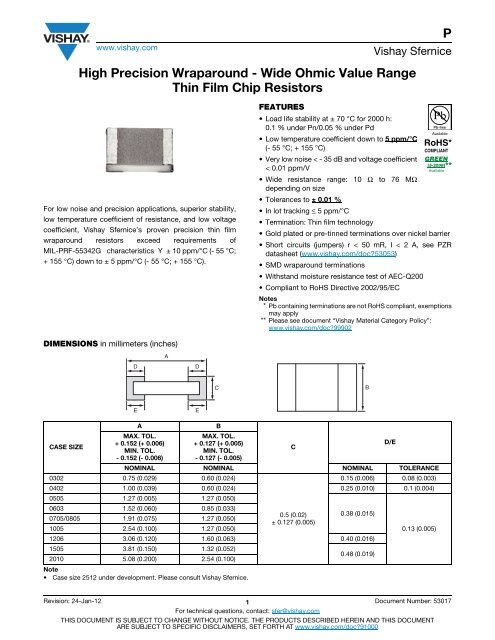
<strong>High</strong> <strong>Precision</strong> <strong>Wraparound</strong> - <strong>Wide</strong> <strong>Ohmic</strong> <strong>Value</strong> Range<br />
Thin Film Chip Resistors<br />
For low noise and precision applications, superior stability,<br />
low temperature coefficient of resistance, and low voltage<br />
coefficient, Vishay Sfernice’s proven precision thin film<br />
wraparound resistors exceed requirements of<br />
MIL-PRF-55342G characteristics Y ± 10 ppm/°C (- 55 °C;<br />
+ 155 °C) down to ± 5 ppm/°C (- 55 °C; + 155 °C).<br />
DIMENSIONS in millimeters (inches)<br />
CASE SIZE<br />
D<br />
E<br />
A B<br />
MAX. TOL.<br />
+ 0.152 (+ 0.006)<br />
MIN. TOL.<br />
- 0.152 (- 0.006)<br />
MAX. TOL.<br />
+ 0.127 (+ 0.005)<br />
MIN. TOL.<br />
- 0.127 (- 0.005)<br />
Note<br />
• Case size 2512 under development. Please consult Vishay Sfernice.<br />
A<br />
D<br />
E<br />
FEATURES<br />
• Load life stability at ± 70 °C for 2000 h:<br />
0.1 % under Pn/0.05 % under Pd<br />
• Low temperature coefficient down to 5 ppm/°C<br />
(- 55 °C; + 155 °C)<br />
• Very low noise < - 35 dB and voltage coefficient<br />
< 0.01 ppm/V<br />
• <strong>Wide</strong> resistance range: 10 Ω to 76 MΩ<br />
depending on size<br />
• Tolerances to ± 0.01 %<br />
• In lot tracking ≤ 5 ppm/°C<br />
• Termination: Thin film technology<br />
• Gold plated or pre-tinned terminations over nickel barrier<br />
• Short circuits (jumpers) r < 50 mR, I < 2 A, see PZR<br />
datasheet (www.vishay.com/doc?53053)<br />
• SMD wraparound terminations<br />
• Withstand moisture resistance test of AEC-Q200<br />
• Compliant to RoHS Directive 2002/95/EC<br />
Notes<br />
* Pb containing terminations are not RoHS compliant, exemptions<br />
may apply<br />
** Please see document “Vishay Material Category Policy”:<br />
www.vishay.com/doc?99902<br />
NOMINAL NOMINAL NOMINAL TOLERANCE<br />
0302 0.75 (0.029) 0.60 (0.024)<br />
0.15 (0.006) 0.08 (0.003)<br />
0402 1.00 (0.039) 0.60 (0.024) 0.25 (0.010) 0.1 (0.004)<br />
0505 1.27 (0.005) 1.27 (0.050)<br />
0603<br />
0705/0805<br />
1.52 (0.060)<br />
1.91 (0.075)<br />
0.85 (0.033)<br />
1.27 (0.050)<br />
0.5 (0.02)<br />
± 0.127 (0.005)<br />
0.38 (0.015)<br />
1005 2.54 (0.100) 1.27 (0.050)<br />
1206 3.06 (0.120) 1.60 (0.063) 0.40 (0.016)<br />
1505<br />
2010<br />
3.81 (0.150)<br />
5.08 (0.200)<br />
1.32 (0.052)<br />
2.54 (0.100)<br />
0.48 (0.019)<br />
C<br />
Revision: 24-Jan-12 1<br />
For technical questions, contact: sfer@vishay.com<br />
Document Number: 53017<br />
THIS DOCUMENT IS SUBJECT TO CHANGE WITHOUT NOTICE. THE PRODUCTS DESCRIBED HEREIN AND THIS DOCUMENT<br />
ARE SUBJECT TO SPECIFIC DISCLAIMERS, SET FORTH AT www.vishay.com/doc?91000<br />
C<br />
B<br />
D/E<br />
0.13 (0.005)
www.vishay.com<br />
SUGGESTED LAND PATTERN (to IPC-7351A)<br />
DIMENSIONS (in millimeter)<br />
CHIP SIZE<br />
Zmax. Gmin. Xmax.<br />
0302 1.30 0.14 0.73<br />
0402 1.55 0.15 0.73<br />
0505 1.82 0.10 1.40<br />
0603 2.37 0.35 0.98<br />
0705/0805 2.76 0.74 1.40<br />
1005 3.39 1.37 1.40<br />
1206 3.91 1.85 1.73<br />
1505 4.66 2.44 1.45<br />
2010 5.93 3.71 2.67<br />
Note<br />
• Case size 2512 under development. Please consult Vishay Sfernice.<br />
ELECTRICAL SPECIFICATIONS<br />
CASE SIZE<br />
Notes<br />
• Case size 2512 under development. Please consult Vishay Sfernice.<br />
(1) Pn = Nominal power - Pd = Derated power intended to improve stability.<br />
(2) For ohmic range versus tolerance and TCR see detailed table on next page.<br />
Z max.<br />
POWER RATING<br />
mW LIMITING ELEMENT VOLTAGE<br />
V<br />
Pn (1) Pd (1)<br />
P<br />
Vishay Sfernice<br />
RESISTANCE RANGE (2)<br />
0302 40 30 25 10 Ω to 750 kΩ<br />
0402 63 40 50 10 Ω to 1.5 MΩ<br />
0505 125 50 50 10 Ω to 4 MΩ<br />
0603 125 100 75 10 Ω to 3.2 MΩ<br />
0705/0805 200 125 150 10 Ω to 10 MΩ<br />
1005 250 125 75 10 Ω to 8.1 MΩ<br />
1206 330 250 200 10 Ω to 35 MΩ<br />
1505 350 175 75 10 Ω to 15 MΩ<br />
2010 1000 500 300 10 Ω to 76 MΩ<br />
G min.<br />
Revision: 24-Jan-12 2<br />
For technical questions, contact: sfer@vishay.com<br />
Document Number: 53017<br />
THIS DOCUMENT IS SUBJECT TO CHANGE WITHOUT NOTICE. THE PRODUCTS DESCRIBED HEREIN AND THIS DOCUMENT<br />
ARE SUBJECT TO SPECIFIC DISCLAIMERS, SET FORTH AT www.vishay.com/doc?91000<br />
X max.
www.vishay.com<br />
ELECTRICAL SPECIFICATIONS<br />
Resistance range: 10 Ω to 76 MΩ<br />
Resistance tolerance: 0.01 % to 1 %<br />
Power dissipation: Pn: 40 mW to 1 W<br />
Pd: 40 mW to 500 mW<br />
Temperature coefficient: Down to 5 ppm - 55 °C; + 155 °C<br />
CLIMATIC SPECIFICATIONS<br />
Operating temp. range: - 55 °C to + 155 °C<br />
For temperature up to 230 °C, see PHT datasheet<br />
(www.vishay.com/doc?53050)<br />
MECHANICAL SPECIFICATIONS<br />
Substrate: Alumina<br />
Technology: Thin film<br />
Film: Nickel chromium with mineral<br />
passivation or CrSi<br />
Protection: Silicone<br />
Terminations: B type: SnPb over nickel barrier<br />
for solder reflow<br />
N type: SnAg over nickel barrier<br />
G type: gold over nickel barrier<br />
for other applications<br />
BEST TOLERANCE AND TCR VS. OHMIC VALUE<br />
STYLE<br />
0302<br />
0402<br />
0505<br />
RANGE<br />
(Ω)<br />
P<br />
Vishay Sfernice<br />
TEMPERATURE COEFFICIENT<br />
TCR CODE FILM<br />
± 5 ppm/°C<br />
Note<br />
(1) R > 39 Ω on request for lower values.<br />
(1) C (- 55 °C; + 155 °C) NiCr<br />
± 5 ppm/°C (1) Z (0 °C; + 70 °C) NiCr<br />
± 10 ppm/°C (1) Y NiCr<br />
± 25 ppm/°C E NiCr<br />
± 50 ppm/°C H NiCr or CrSi<br />
± 100 ppm/°C K NiCr or CrSi<br />
POWER DERATING CURVE<br />
0<br />
0 20 40 60 70 80 100 120 140 155<br />
Revision: 24-Jan-12 3<br />
For technical questions, contact: sfer@vishay.com<br />
Document Number: 53017<br />
THIS DOCUMENT IS SUBJECT TO CHANGE WITHOUT NOTICE. THE PRODUCTS DESCRIBED HEREIN AND THIS DOCUMENT<br />
ARE SUBJECT TO SPECIFIC DISCLAIMERS, SET FORTH AT www.vishay.com/doc?91000<br />
Rated Power (%)<br />
100<br />
80<br />
60<br />
40<br />
20<br />
TOLERANCE<br />
(± %)<br />
Ambient Temperature in °C<br />
TCR CODE<br />
10 to < 100 0.05; 0.1; 0.25; 0.5; 1; 2; 5 C; Z; Y; E; H; K<br />
100 to 35K 0.01; 0.02; 0.05; 0.1; 0.25; 0.5; 1; 2; 5 C; Z; Y; E; H; K<br />
> 35K to 50K 0.01; 0.02; 0.05; 0.1; 0.25; 0.5; 1; 2; 5 Z; Y; E; H; K<br />
> 50K to 75K 0.05; 0.1; 0.25; 0.5; 1; 2; 5 E; H; K<br />
> 75K to 750K 0.1; 0.25; 0.5; 1; 2; 5 (1) H; K<br />
10 to < 100 0.05; 0.1; 0.25; 0.5; 1; 2; 5 C; Z; Y; E; H; K<br />
100 to 67K 0.01; 0.02; 0.05; 0.1; 0.25; 0.5; 1; 2; 5 C; Z; Y; E; H; K<br />
> 67K to 100K 0.01; 0.02; 0.05; 0.1; 0.25; 0.5; 1; 2; 5 Z; Y; E; H; K<br />
> 100K to 150K 0.05; 0.1; 0.25; 0.5; 1; 2; 5 E; H; K<br />
> 150K to 1M5 0.1; 0.25; 0.5; 1; 2; 5 (1) H; K<br />
10 to < 100 0.05; 0.1; 0.25; 0.5; 1; 2; 5 C; Z; Y; E; H; K<br />
100 to 187K 0.01; 0.02; 0.05; 0.1; 0.25; 0.5; 1; 2; 5 C; Z; Y; E; H; K<br />
> 187K to 260K 0.01; 0.02; 0.05; 0.1; 0.25; 0.5; 1; 2; 5 Z; Y; E; H; K<br />
> 260K to 400K 0.05; 0.1; 0.25; 0.5; 1; 2; 5 E; H; K<br />
> 400K to 4M 0.1; 0.25; 0.5; 1; 2; 5 (1) H; K
www.vishay.com<br />
BEST TOLERANCE AND TCR VS. OHMIC VALUE<br />
STYLE<br />
0603<br />
0805<br />
1005<br />
1206<br />
1505<br />
2010<br />
Note<br />
• Tolerance 0.05 % on request<br />
RANGE<br />
(Ω)<br />
TOLERANCE<br />
(± %)<br />
P<br />
Vishay Sfernice<br />
TCR CODE<br />
10 to < 100 0.05; 0.1; 0.25; 0.5; 1; 2; 5 C; Z; Y; E; H; K<br />
100 to 160K 0.01; 0.02; 0.05; 0.1; 0.25; 0.5; 1; 2; 5 C; Z; Y; E; H; K<br />
> 160K to 332K 0.01; 0.02; 0.05; 0.1; 0.25; 0.5; 1; 2; 5 Z; Y; E; H; K<br />
> 332K to 500K 0.05; 0.1; 0.25; 0.5; 1; 2; 5 (1) E; H; K<br />
> 500K to 3M2 0.1; 0.25; 0.5; 1; 2; 5 H; K<br />
10 to < 100 0.05; 0.1; 0.25; 0.5; 1; 2; 5 C; Z; Y; E; H; K<br />
100 to 360K 0.01; 0.02; 0.05; 0.1; 0.25; 0.5; 1; 2; 5 C; Z; Y; E; H; K<br />
> 360K to 511K 0.01; 0.02; 0.05; 0.1; 0.25; 0.5; 1; 2; 5 Z; Y; E; H; K<br />
> 511K to 750K 0.05; 0.1; 0.25; 0.5; 1; 2; 5 E; H; K<br />
> 750K to 10M 0.1; 0.25; 0.5; 1; 2; 5 (1) H; K<br />
10 to < 100 0.05; 0.1; 0.25; 0.5; 1; 2; 5 C; Z; Y; E; H; K<br />
100 to 400K 0.01; 0.02; 0.05; 0.1; 0.25; 0.5; 1; 2; 5 C; Z; Y; E; H; K<br />
> 400K to 550K 0.01; 0.02; 0.05; 0.1; 0.25; 0.5; 1; 2; 5 Z; Y; E; H; K<br />
> 550K to 810K 0.05; 0.1; 0.25; 0.5; 1; 2; 5 E; H; K<br />
> 810K to 8M1 0.1; 0.25; 0.5; 1; 2; 5 (1) H; K<br />
10 to < 100 0.05; 0.1; 0.25; 0.5; 1; 2; 5 C; Z; Y; E; H; K<br />
100 to 1M3 0.01; 0.02; 0.05; 0.1; 0.25; 0.5; 1; 2; 5 C; Z; Y; E; H; K<br />
> 1M3 to 2M 0.01; 0.02; 0.05; 0.1; 0.25; 0.5; 1; 2; 5 Z; Y; E; H; K<br />
> 2M to 3M5 0.05; 0.1; 0.25; 0.5; 1; 2; 5 E; H; K<br />
> 3M5 to 35M 0.1; 0.25; 0.5; 1; 2; 5 (1) H; K<br />
10 to < 100 0.05; 0.1; 0.25; 0.5; 1; 2; 5 C; Z; Y; E; H; K<br />
100 to 720K 0.01; 0.02; 0.05; 0.1; 0.25; 0.5; 1; 2; 5 C; Z; Y; E; H; K<br />
> 720K to 1M 0.01; 0.02; 0.05; 0.1; 0.25; 0.5; 1; 2; 5 Z; Y; E; H; K<br />
> 1M to 1M5 0.05; 0.1; 0.25; 0.5; 1; 2; 5 E; H; K<br />
> 1M5 to 15M 0.1; 0.25; 0.5; 1; 2; 5 (1) H; K<br />
10 to < 100 0.05; 0.1; 0.25; 0.5; 1; 2; 5 C; Z; Y; E; H; K<br />
100 to 3M8 0.01; 0.02; 0.05; 0.1; 0.25; 0.5; 1; 2; 5 C; Z; Y; E; H; K<br />
> 3M8 to 5M 0.01; 0.02; 0.05; 0.1; 0.25; 0.5; 1; 2; 5 Z; Y; E; H; K<br />
> 5M to 7M5 0.05; 0.1; 0.25; 0.5; 1; 2; 5 E; H; K<br />
> 7M5 to 76M 0.1; 0.25; 0.5; 1; 2; 5 (1) H; K<br />
Revision: 24-Jan-12 4<br />
For technical questions, contact: sfer@vishay.com<br />
Document Number: 53017<br />
THIS DOCUMENT IS SUBJECT TO CHANGE WITHOUT NOTICE. THE PRODUCTS DESCRIBED HEREIN AND THIS DOCUMENT<br />
ARE SUBJECT TO SPECIFIC DISCLAIMERS, SET FORTH AT www.vishay.com/doc?91000
POPULAR OPTIONS<br />
www.vishay.com<br />
P<br />
Vishay Sfernice<br />
For any option it is recommended to consult Vishay Sfernice for availability first.<br />
Option: Enlarged terminations<br />
For stringent and special power dissipation requirements, the thermal resistance between the resistive layer and the solder joint<br />
can be reduced using enlarged terminations chip resistors which are soldered on large and thick copper pads acting as heatsink<br />
(see application note: 53048 Power Dissipation in <strong>High</strong> <strong>Precision</strong> Vishay Sfernice Chip Resistors and Arrays (P Thin Film, PRA<br />
Arrays, CHP Thick Film) www.vishay.com/doc?53048.<br />
Option to order 0063: (applies to size 1206/1505/2010).<br />
DIMENSIONS (Option 0063) in millimeters<br />
CASE SIZE<br />
A B E D<br />
MAX. TOL.<br />
+ 0.152<br />
MIN. TOL.<br />
- 0.152<br />
Enlarged<br />
termination<br />
MAX. TOL.<br />
+ 0.127<br />
MIN. TOL.<br />
- 0.127<br />
Note<br />
• Case size 2512 under development. Please consult Vishay Sfernice.<br />
SUGGESTED LAND PATTERN (Option 0063)<br />
MAX. TOL.<br />
+ 0.13<br />
MIN. TOL.<br />
- 0.13<br />
Note<br />
• Case size 2512 under development. Please consult Vishay Sfernice.<br />
E<br />
Bottom view for mounting<br />
F<br />
MAX. TOL.<br />
+ 0.13<br />
MIN. TOL.<br />
- 0.13<br />
NOMINAL NOMINAL NOMINAL NOMINAL NOMINAL MIN. MAX.<br />
1206 3.06 1.60 0.40 1.215<br />
1505<br />
2010<br />
3.81<br />
5.08<br />
1.32<br />
2.54<br />
0.48<br />
1.59<br />
2.25<br />
0.63 0.50 0.76<br />
Z max.<br />
DIMENSIONS (IN MILLIMETER)<br />
CHIP SIZE<br />
Zmax. Gmin. Xmax.<br />
1206 3.91<br />
1.73<br />
1505 4.66 0.50<br />
1.45<br />
2010 5.93 2.67<br />
G min.<br />
Revision: 24-Jan-12 5<br />
For technical questions, contact: sfer@vishay.com<br />
Document Number: 53017<br />
THIS DOCUMENT IS SUBJECT TO CHANGE WITHOUT NOTICE. THE PRODUCTS DESCRIBED HEREIN AND THIS DOCUMENT<br />
ARE SUBJECT TO SPECIFIC DISCLAIMERS, SET FORTH AT www.vishay.com/doc?91000<br />
A<br />
D<br />
B<br />
Uncoatted<br />
ceramic<br />
X max.<br />
F
www.vishay.com<br />
Option: Marking<br />
Option to order 0013:<br />
Marking of ohmic value and tolerance:<br />
Sizes: 0805 to 1005: 3 digits marking (according to EIA-96)<br />
Sizes: 1206 to 2010: 4 digits marking (same codification than in the ordering procedure)<br />
Tolerance indicated by a color dot.<br />
Option to order 0014:<br />
Marking of ohmic value:<br />
Sizes: 0805 to 1005: 3 digits marking (according to EIA-96)<br />
Sizes: 1206 to 2010: 4 digits marking (same codification than in the ordering procedure)<br />
No standard marking available for smaller sizes.<br />
A price adder will apply to the unit price of the parts for options 0013 and 0014.<br />
Option: AEC-Q200<br />
Moisture resistance<br />
Option to Order 0058:<br />
Specific production process to withstand 85 °C/85 % at Pn/10<br />
PACKAGING<br />
ESD packaging available: waffle-pack, and plastic tape and<br />
reel (low conductivity). Paper tape available upon request<br />
(ESD only) (for size 0603, 0805, and 1206).<br />
NUMBER OF PIECES PER PACKAGE<br />
SIZE<br />
0302<br />
MOQ WAFFLE PACK<br />
2" × 2"<br />
TAPE AND REEL<br />
MIN. MAX.<br />
TAPE<br />
WIDTH<br />
0402<br />
0505<br />
0603<br />
100<br />
5000<br />
0805<br />
0705<br />
100<br />
100<br />
8 mm<br />
1005 221<br />
4000<br />
1206 140<br />
1505<br />
2010<br />
60<br />
100 2000 8 mm<br />
PERFORMANCE<br />
TESTS CONDITIONS<br />
Thermal shock<br />
Short time overload<br />
Low temperature operation<br />
Resistance to solder heat<br />
Moisture resistance<br />
<strong>High</strong> temperature<br />
Load life<br />
Notes<br />
(1) 0.05 % under Pd<br />
(2) Option to order<br />
P<br />
Vishay Sfernice<br />
PACKAGING RULES<br />
Waffle Pack<br />
Can be filled up to maximum quantity indicated in the table<br />
here above, taking into account the minimum order quantity.<br />
When quantity ordered exceeds maximum quantity of a<br />
single waffle pack, the waffle packs are stacked up on the<br />
top of each other and closed by one single cover.<br />
To get “not stacked up” waffle pack in case of ordered<br />
quantity > maximum number of pieces per package:<br />
Please consult Vishay Sfernice for specific ordering<br />
code.<br />
Tape and Reel<br />
Can be filled up to maximum quantity indicated in the table<br />
here above, taking into account the minimum order quantity.<br />
When quantity ordered is between the MOQ and the<br />
maximum reel capacity, only one reel is provided.<br />
When several reels are needed for ordered quantity<br />
within MOQ and maximum reel capacity: Please consult<br />
Vishay Sfernice for specific ordering code.<br />
MIL OR CECC<br />
REQUIREMENTS<br />
TYPICAL<br />
PERFORMANCES<br />
MIL-PRF-55342G<br />
MIL-STD-202 F-Method 107 F<br />
± 0.05 % ± 0.02 %<br />
MIL-PRF-55342G<br />
PARA 3.10.4.7.5<br />
± 0.05 % ± 0.01 %<br />
MIL-PRF-55342G<br />
PARA 3.9 and 4.7.4<br />
± 0.05 % ± 0.01 %<br />
MIL-PRF-55342G<br />
PARA 3.12, 4.7.7, 4.7.1.2<br />
MIL-PRF-55342G<br />
± 0.05 % ± 0.03 %<br />
PARA 3.13 and 4.7.8<br />
MIL-STD-202 F-Method 106 E<br />
± 0.10 % ± 0.01 %<br />
CECC 56 days/40 °C/93 % RH<br />
AEC-Q200<br />
± 0.10 % ± 0.01 %<br />
(2)<br />
85 °C/85 % RH/Pn/10<br />
1000 h<br />
± 0.5 % + 0.05 Ω Max. < 0.3 % + 0.05 Ω<br />
MIL-PRF-55342G<br />
PARA 3.11 and 4.7.6<br />
MIL-PRF-55342G<br />
± 0.05 % ± 0.05 %<br />
2000 h Pn at 70 °C<br />
MIL-STD-202 F-Method 108 A<br />
± 0.5 % ± 0.10 % (1)<br />
Revision: 24-Jan-12 6<br />
For technical questions, contact: sfer@vishay.com<br />
Document Number: 53017<br />
THIS DOCUMENT IS SUBJECT TO CHANGE WITHOUT NOTICE. THE PRODUCTS DESCRIBED HEREIN AND THIS DOCUMENT<br />
ARE SUBJECT TO SPECIFIC DISCLAIMERS, SET FORTH AT www.vishay.com/doc?91000
Permissible Pulse Power P (W)<br />
Permissible Pulse Energy (J)<br />
www.vishay.com<br />
100<br />
10<br />
1<br />
Maximum permissible pulse load Pi max. for single pulse<br />
0.1<br />
0.00001 0.0001 0.001 0.01 0.1 1 10<br />
100<br />
10<br />
1<br />
Pulse Duration t (s)<br />
Energy for single pulse<br />
Maximum permissible pulse voltage Ui max.<br />
P<br />
Vishay Sfernice<br />
Revision: 24-Jan-12 7<br />
For technical questions, contact: sfer@vishay.com<br />
Document Number: 53017<br />
THIS DOCUMENT IS SUBJECT TO CHANGE WITHOUT NOTICE. THE PRODUCTS DESCRIBED HEREIN AND THIS DOCUMENT<br />
ARE SUBJECT TO SPECIFIC DISCLAIMERS, SET FORTH AT www.vishay.com/doc?91000<br />
P2512<br />
P2010<br />
P1206<br />
P0805<br />
P0603<br />
P0402<br />
0.00001<br />
0.00001 0.0001 0.001 0.01 0.1 1 10<br />
Permissible Pulse Voltage (V)<br />
0.1<br />
0.01<br />
0.001<br />
0.0001<br />
10 000<br />
1000<br />
100<br />
Pulse Duration t (s)<br />
P2512<br />
P2010<br />
P1206<br />
P0805<br />
P0603<br />
P0402<br />
10<br />
0.00001 0.0001 0.001 0.01 0.1 1 10<br />
Pulse Duration t (s)<br />
P2512<br />
P2010<br />
P1206<br />
P0805<br />
P0603<br />
P0402
Permissible Pulse Power P (W)<br />
Test Voltage (V)<br />
Test Voltage (V)<br />
www.vishay.com<br />
100<br />
10<br />
1<br />
Maximum permissible pulse load Pi max.<br />
0.1<br />
0.00001 0.0001 0.001 0.01 0.1 1 10<br />
10 000<br />
1000<br />
100<br />
10 000<br />
Pulse Duration t (s)<br />
1.2/50 μs lightning surge<br />
10/700 μs lightning surge<br />
P<br />
Vishay Sfernice<br />
Revision: 24-Jan-12 8<br />
For technical questions, contact: sfer@vishay.com<br />
Document Number: 53017<br />
THIS DOCUMENT IS SUBJECT TO CHANGE WITHOUT NOTICE. THE PRODUCTS DESCRIBED HEREIN AND THIS DOCUMENT<br />
ARE SUBJECT TO SPECIFIC DISCLAIMERS, SET FORTH AT www.vishay.com/doc?91000<br />
P2512<br />
P2010<br />
P1206<br />
P0805<br />
P0603<br />
P0402<br />
10<br />
10 100 1000 10 000 100 000<br />
1000<br />
100<br />
Resistor <strong>Value</strong> (Ω)<br />
P2512<br />
P1206<br />
P0805<br />
P0603<br />
10<br />
10 100 1000 10 000 100 000<br />
Resistor <strong>Value</strong> (Ω)<br />
P1206<br />
P0805<br />
P0603
www.vishay.com<br />
GLOBAL PART NUMBER INFORMATION<br />
New Global Part Numbering: P0505Y1003BBT0999<br />
Notes<br />
(1) For specific quantity of parts per packaging please consult Vishay Sfernice.<br />
(2) For paper tape please consult Vishay Sfernice (0603, 0805, and 1206 only).<br />
QUICK PROTOTYPING<br />
P<br />
Vishay Sfernice<br />
Vishay Sfernice can offer quick prototyping service in 3 weeks production time for most popular case sizes: 0603, 0805, 1206<br />
(Best tolerance: 0.05 %, best TCR: 10 ppm/°C) - Premium will apply - Check availability<br />
PTRIM<br />
P 0 5 0 5 Y 1 0 0 3 B B T 0 9 9 9<br />
GLOBAL MODEL SIZE TCR VALUE TOLERANCE TERMINATION PACKAGING OPTION<br />
P 0302<br />
0402<br />
0505<br />
0603<br />
0705<br />
0805<br />
1005<br />
1206<br />
1505<br />
2010<br />
K =<br />
± 100 ppm/°C<br />
H = ± 50 ppm/°C<br />
E = ± 25 ppm/°C<br />
Y = ± 10 ppm/°C<br />
Z = ± 5 ppm<br />
(0.70 °C)<br />
C = ± 5 ppm<br />
(- 55 °C; + 155 °C)<br />
The first three digits<br />
are significant figures<br />
and the last digit<br />
specifies the number<br />
of zeros to follow,<br />
R designates<br />
decimal point<br />
10R0 = 10 Ω<br />
3901 = 3900 Ω<br />
1004 = 1 MΩ<br />
Historical Part Number example: P 0505 Y 1003 B B TR R0999 e2<br />
Chips ready to be trimmed available. Please consult Vishay Sfernice.<br />
L = ± 0.01 %<br />
P = ± 0.02 %<br />
W = ± 0.05 %<br />
B = ± 0.1 %<br />
C = ± 0.25 %<br />
D = ± 0.5 %<br />
F = ± 1 %<br />
G = ± 2 %<br />
J = ± 5 %<br />
B: SnPb over<br />
nickel barrier<br />
N: SnAg over<br />
nickel barrier<br />
G: Gold over<br />
nickel barrier<br />
Blank =<br />
Waffle pack<br />
T = Tape (1)<br />
PT = Paper<br />
tape (2)<br />
Notes<br />
• For CECC qualified, see RV datasheet (www.vishay.com/doc?60022)<br />
• For ESCC qualified, see PHR datasheet (www.vishay.com/doc?53037) or PFRR datasheet (www.vishay.com/doc?53046)<br />
• For <strong>High</strong> Temperature (230 °C), see PHT datasheet (www.vishay.com/doc?53050)<br />
• For Strap (0 Ω), see PZR datasheet (www.vishay.com/doc?53053)<br />
Leave<br />
blank if no<br />
option<br />
B: Lead bearing version<br />
N and G: Lead (Pb)-free/RoHS version<br />
P 0505 Y 1003 B B TR R0999 e2<br />
HISTORICAL<br />
MODEL<br />
P 0302<br />
0402<br />
0505<br />
0603<br />
0705<br />
0805<br />
1005<br />
1206<br />
1505<br />
2010<br />
SIZE TCR VALUE TOLERANCE TERMINATION PACKAGING OPTION RoHS<br />
K =<br />
± 100 ppm/°C<br />
H = ± 50 ppm/°C<br />
E = ± 25 ppm/°C<br />
Y = ± 10 ppm/°C<br />
Z = ± 5 ppm<br />
(0.70 °C)<br />
C = ± 5 ppm<br />
(- 55 °C; + 155 °C)<br />
The first three<br />
digits are<br />
significant figures<br />
and the last digit<br />
specifies the<br />
number of zeros<br />
to follow,<br />
R designates<br />
decimal point<br />
10R0 = 10 Ω<br />
3901 = 3900 Ω<br />
1004 = 1 MΩ<br />
L = ± 0.01 %<br />
P = ± 0.02 %<br />
W = ± 0.05 %<br />
B = ± 0.1 %<br />
C = ± 0.25 %<br />
D = ± 0.5 %<br />
F = ± 1 %<br />
G = ± 2 %<br />
J = ± 5 %<br />
B: SnPb over<br />
nickel barrier<br />
N: SnAg over<br />
nickel barrier<br />
G: Gold over<br />
nickel barrier<br />
Blank =<br />
Waffle pack<br />
TR = Tape (1)<br />
B: Lead bearing version<br />
N and G: Lead (Pb)-free/RoHS version<br />
Leave blank<br />
if no option<br />
e2:<br />
Tin/silver<br />
e4:<br />
Gold<br />
Blank:<br />
SnPb<br />
Revision: 24-Jan-12 9<br />
For technical questions, contact: sfer@vishay.com<br />
Document Number: 53017<br />
THIS DOCUMENT IS SUBJECT TO CHANGE WITHOUT NOTICE. THE PRODUCTS DESCRIBED HEREIN AND THIS DOCUMENT<br />
ARE SUBJECT TO SPECIFIC DISCLAIMERS, SET FORTH AT www.vishay.com/doc?91000
www.vishay.com<br />
Disclaimer<br />
Legal Disclaimer Notice<br />
Vishay<br />
ALL PRODUCT, PRODUCT SPECIFICATIONS AND DATA ARE SUBJECT TO CHANGE WITHOUT NOTICE TO IMPROVE<br />
RELIABILITY, FUNCTION OR DESIGN OR OTHERWISE.<br />
Vishay Intertechnology, Inc., its affiliates, agents, and employees, and all persons acting on its or their behalf (collectively,<br />
“Vishay”), disclaim any and all liability for any errors, inaccuracies or incompleteness contained in any datasheet or in any other<br />
disclosure relating to any product.<br />
Vishay makes no warranty, representation or guarantee regarding the suitability of the products for any particular purpose or<br />
the continuing production of any product. To the maximum extent permitted by applicable law, Vishay disclaims (i) any and all<br />
liability arising out of the application or use of any product, (ii) any and all liability, including without limitation special,<br />
consequential or incidental damages, and (iii) any and all implied warranties, including warranties of fitness for particular<br />
purpose, non-infringement and merchantability.<br />
Statements regarding the suitability of products for certain types of applications are based on Vishay’s knowledge of typical<br />
requirements that are often placed on Vishay products in generic applications. Such statements are not binding statements<br />
about the suitability of products for a particular application. It is the customer’s responsibility to validate that a particular<br />
product with the properties described in the product specification is suitable for use in a particular application. Parameters<br />
provided in datasheets and/or specifications may vary in different applications and performance may vary over time. All<br />
operating parameters, including typical parameters, must be validated for each customer application by the customer’s<br />
technical experts. Product specifications do not expand or otherwise modify Vishay’s terms and conditions of purchase,<br />
including but not limited to the warranty expressed therein.<br />
Except as expressly indicated in writing, Vishay products are not designed for use in medical, life-saving, or life-sustaining<br />
applications or for any other application in which the failure of the Vishay product could result in personal injury or death.<br />
Customers using or selling Vishay products not expressly indicated for use in such applications do so at their own risk and agree<br />
to fully indemnify and hold Vishay and its distributors harmless from and against any and all claims, liabilities, expenses and<br />
damages arising or resulting in connection with such use or sale, including attorneys fees, even if such claim alleges that Vishay<br />
or its distributor was negligent regarding the design or manufacture of the part. Please contact authorized Vishay personnel to<br />
obtain written terms and conditions regarding products designed for such applications.<br />
No license, express or implied, by estoppel or otherwise, to any intellectual property rights is granted by this document or by<br />
any conduct of Vishay. Product names and markings noted herein may be trademarks of their respective owners.<br />
Material Category Policy<br />
Vishay Intertechnology, Inc. hereby certifies that all its products that are identified as RoHS-Compliant fulfill the<br />
definitions and restrictions defined under Directive 2011/65/EU of The <strong>Europe</strong>an Parliament and of the Council<br />
of June 8, 2011 on the restriction of the use of certain hazardous substances in electrical and electronic equipment<br />
(EEE) - recast, unless otherwise specified as non-compliant.<br />
Please note that some Vishay documentation may still make reference to RoHS Directive 2002/95/EC. We confirm that<br />
all the products identified as being compliant to Directive 2002/95/EC conform to Directive 2011/65/EU.<br />
Revision: 12-Mar-12 1 Document Number: 91000