Silicon PIN Photodiode VBP104S, VBP104SR
Silicon PIN Photodiode VBP104S, VBP104SR
Silicon PIN Photodiode VBP104S, VBP104SR

Create successful ePaper yourself
Turn your PDF publications into a flip-book with our unique Google optimized e-Paper software.
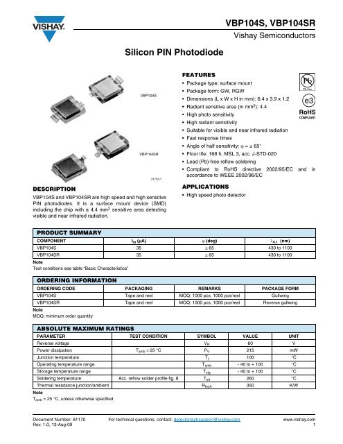
DESCRIPTION<br />
<strong>VBP104S</strong> and <strong>VBP104S</strong>R are high speed and high sensitive<br />
<strong>PIN</strong> photodiodes. It is a surface mount device (SMD)<br />
including the chip with a 4.4 mm 2 sensitive area detecting<br />
visible and near infrared radiation.<br />
<strong>Silicon</strong> <strong>PIN</strong> <strong>Photodiode</strong><br />
<strong>VBP104S</strong>, <strong>VBP104S</strong>R<br />
Vishay Semiconductors<br />
FEATURES<br />
• Package type: surface mount<br />
Package form: GW, RGW<br />
Dimensions (L x W x H in mm): 6.4 x 3.9 x 1.2<br />
Radiant sensitive area (in mm2 ): 4.4<br />
High photo sensitivity<br />
High radiant sensitivity<br />
Suitable for visible and near infrared radiation<br />
Fast response times<br />
Angle of half sensitivity: ϕ = ± 65°<br />
Floor life: 168 h, MSL 3, acc. J-STD-020<br />
Lead (Pb)-free reflow soldering<br />
Compliant to RoHS directive 2002/95/EC and in<br />
accordance to WEEE 2002/96/EC<br />
APPLICATIONS<br />
High speed photo detector<br />
PRODUCT SUMMARY<br />
COMPONENT Ira (µA) ϕ (deg) λ0.1 (nm)<br />
<strong>VBP104S</strong> 35 ± 65 430 to 1100<br />
<strong>VBP104S</strong>R<br />
Note<br />
Test conditions see table “Basic Characteristics”<br />
35 ± 65 430 to 1100<br />
Note<br />
MOQ: minimum order quantity<br />
Note<br />
Tamb = 25 °C, unless otherwise specified<br />
<strong>VBP104S</strong><br />
<strong>VBP104S</strong>R<br />
21733-1<br />
ORDERING INFORMATION<br />
ORDERING CODE PACKAGING REMARKS PACKAGE FORM<br />
<strong>VBP104S</strong> Tape and reel MOQ: 1000 pcs, 1000 pcs/reel Gullwing<br />
<strong>VBP104S</strong>R Tape and reel MOQ: 1000 pcs, 1000 pcs/reel Reverse gullwing<br />
ABSOLUTE MAXIMUM RATINGS<br />
PARAMETER TEST CONDITION SYMBOL VALUE UNIT<br />
Reverse voltage VR 60 V<br />
Power dissipation Tamb ≤ 25 °C PV 215 mW<br />
Junction temperature Tj 100 °C<br />
Operating temperature range Tamb - 40 to + 100 °C<br />
Storage temperature range Tstg - 40 to + 100 °C<br />
Soldering temperature Acc. reflow solder profile fig. 8 Tsd 260 °C<br />
Thermal resistance junction/ambient RthJA 350 K/W<br />
Document Number: 81170 For technical questions, contact: detectortechsupport@vishay.com www.vishay.com<br />
Rev. 1.0, 13-Aug-09 1
<strong>VBP104S</strong>, <strong>VBP104S</strong>R<br />
Vishay Semiconductors<br />
BASIC CHARACTERISTICS<br />
Note<br />
Tamb = 25 °C, unless otherwise specified<br />
BASIC CHARACTERISTICS<br />
Tamb = 25 °C, unless otherwise specified<br />
<strong>Silicon</strong> <strong>PIN</strong> <strong>Photodiode</strong><br />
PARAMETER TEST CONDITION SYMBOL MIN. TYP. MAX. UNIT<br />
Forward voltage IF = 50 mA VF 1 1.3 V<br />
Breakdown voltage IR = 100 µA, E = 0 V(BR) 60 V<br />
Reverse dark current VR = 10 V, E = 0 Iro 2 30 nA<br />
Diode capacitance<br />
VR = 0 V, f = 1 MHz, E = 0<br />
VR = 3 V, f = 1 MHz, E = 0<br />
CD<br />
CD<br />
48<br />
17 40<br />
pF<br />
pF<br />
Open circuit voltage Ee = 1 mW/cm2 , λ = 950 nm Vo 350 mV<br />
Temperature coefficient of Vo Ee = 1 mW/cm2 , λ = 950 nm TKVo - 2.6 mV/K<br />
Short circuit current Ee = 1 mW/cm2 , λ = 950 nm Ik 32 µA<br />
Temperature coefficient of Ik Ee = 1 mW/cm2 , λ = 950 nm TKIk 0.1 %/K<br />
Reverse light current<br />
Ee = 1 mW/cm2 , λ = 950 nm,<br />
VR = 5 V<br />
Ira 25 35 µA<br />
Angle of half sensitivity ϕ ± 65 deg<br />
Wavelength of peak sensitivity λp 940 nm<br />
Range of spectral bandwidth λ0.1 430 to 1100 nm<br />
Noise equivalent power VR = 10 V, λ = 950 nm NEP 4 x 10-14 W/√Hz<br />
Rise time<br />
Fall time<br />
I ro - Reverse Dark Current (nA)<br />
1000<br />
100<br />
10<br />
V R = 10 V<br />
VR = 10 V, RL = 1 kΩ,<br />
λ = 820 nm<br />
VR = 10 V, RL = 1 kΩ,<br />
λ = 820 nm<br />
tr 100 ns<br />
tf 100 ns<br />
1<br />
0.6<br />
20 40 60 80 100<br />
0 20 40 60 80 100<br />
94 8403 Tamb - Ambient Temperature (°C)<br />
94 8409 T amb - Ambient Temperature (°C)<br />
Fig. 1 - Reverse Dark Current vs. Ambient Temperature Fig. 2 - Relative Reverse Light Current vs. Ambient Temperature<br />
www.vishay.com For technical questions, contact: detectortechsupport@vishay.com Document Number: 81170<br />
2 Rev. 1.0, 13-Aug-09<br />
I - Relative Reverse Light Current<br />
ra rel<br />
1.4<br />
1.2<br />
1.0<br />
0.8<br />
VR =5V<br />
λ = 950 nm
I ra - Reverse Light Current (µA)<br />
0.1<br />
0.01 0.1 1<br />
94 8421<br />
Ee - Irradiance (mW/cm ) 2<br />
I ra - Reverse Light Current (µA)<br />
C D - Diode Capacitance (pF)<br />
1000<br />
100<br />
10<br />
1<br />
100<br />
Fig. 3 - Reverse Light Current vs. Irradiance<br />
10<br />
94 8422<br />
1<br />
0.1 1 10<br />
VR =5V<br />
λ= 950 nm<br />
Fig. 4 - Reverse Light Current vs. Reverse Voltage<br />
80<br />
60<br />
40<br />
20<br />
94 8423<br />
λ = 950 nm<br />
1 mW/cm 2<br />
0.5 mW/cm 2<br />
0.2 mW/cm 2<br />
0.1 mW/cm 2<br />
0.05 mW/cm 2<br />
V R - Reverse Voltage (V)<br />
E = 0<br />
f = 1 MHz<br />
0<br />
0.1 1 10<br />
V R - Reverse Voltage (V)<br />
Fig. 5 - Diode Capacitance vs. Reverse Voltage<br />
10<br />
100<br />
100<br />
<strong>VBP104S</strong>, <strong>VBP104S</strong>R<br />
<strong>Silicon</strong> <strong>PIN</strong> <strong>Photodiode</strong> Vishay Semiconductors<br />
0<br />
350 550 750 950<br />
Fig. 6 - Relative Spectral Sensitivity vs. Wavelength<br />
Fig. 7 - Relative Radiant Sensitivity vs. Angular Displacement<br />
Document Number: 81170 For technical questions, contact: detectortechsupport@vishay.com www.vishay.com<br />
Rev. 1.0, 13-Aug-09 3<br />
S(λ) rel - Relative Spectral Sensitivity<br />
S rel - Relative Radiant Sensitivity<br />
1.0<br />
0.8<br />
0.6<br />
0.4<br />
0.2<br />
94 8420 λ - Wavelength (nm)<br />
1.0<br />
0.9<br />
0.8<br />
0.7<br />
94 8406<br />
0.6<br />
0°<br />
0.4 0.2 0<br />
10° 20°<br />
1150<br />
30°<br />
40°<br />
50°<br />
60°<br />
70°<br />
80°<br />
ϕ - Angular Displacement
<strong>VBP104S</strong>, <strong>VBP104S</strong>R<br />
Vishay Semiconductors<br />
<strong>Silicon</strong> <strong>PIN</strong> <strong>Photodiode</strong><br />
PACKAGE DIMENSIONS FOR <strong>VBP104S</strong> in millimeters<br />
PACKAGE DIMENSIONS FOR <strong>VBP104S</strong>R in millimeters<br />
www.vishay.com For technical questions, contact: detectortechsupport@vishay.com Document Number: 81170<br />
4 Rev. 1.0, 13-Aug-09<br />
21728<br />
21729
TA<strong>PIN</strong>G DIMENSIONS FOR <strong>VBP104S</strong> in millimeters<br />
TA<strong>PIN</strong>G DIMENSIONS FOR <strong>VBP104S</strong>R in millimeters<br />
21731<br />
21730<br />
<strong>VBP104S</strong>, <strong>VBP104S</strong>R<br />
<strong>Silicon</strong> <strong>PIN</strong> <strong>Photodiode</strong> Vishay Semiconductors<br />
Document Number: 81170 For technical questions, contact: detectortechsupport@vishay.com www.vishay.com<br />
Rev. 1.0, 13-Aug-09 5
<strong>VBP104S</strong>, <strong>VBP104S</strong>R<br />
Vishay Semiconductors<br />
<strong>Silicon</strong> <strong>PIN</strong> <strong>Photodiode</strong><br />
REEL DIMENSIONS FOR <strong>VBP104S</strong> AND <strong>VBP104S</strong>R in millimeters<br />
SOLDER PROFILE<br />
Temperature (°C)<br />
19841<br />
300<br />
250<br />
200<br />
150<br />
100<br />
50<br />
21732<br />
255 °C<br />
240 °C<br />
217 °C<br />
max. 120 s<br />
0<br />
0 50 100 150 200 250 300<br />
Time (s)<br />
max. 30 s<br />
max. 100 s<br />
max. 260 °C<br />
245 °C<br />
max. ramp up 3 °C/s max. ramp down 6 °C/s<br />
Fig. 8 - Lead (Pb)-free Reflow Solder Profile<br />
acc. J-STD-020<br />
DRYPACK<br />
Devices are packed in moisture barrier bags (MBB) to<br />
prevent the products from moisture absorption during<br />
transportation and storage. Each bag contains a desiccant.<br />
FLOOR LIFE<br />
Time between soldering and removing from MBB must not<br />
exceed the time indicated in J-STD-020:<br />
Moisture sensitivity: level 3<br />
Floor life: 168 h<br />
Conditions: Tamb < 30 °C, RH < 60 %<br />
DRYING<br />
In case of moisture absorption devices should be baked<br />
before soldering. Conditions see J-STD-020 or<br />
recommended conditions:<br />
192 h at 40 °C (+ 5 °C), RH < 5 %<br />
or<br />
96 h at 60 °C (+ 5 °C), RH < 5 %.<br />
www.vishay.com For technical questions, contact: detectortechsupport@vishay.com Document Number: 81170<br />
6 Rev. 1.0, 13-Aug-09
Disclaimer<br />
All product specifications and data are subject to change without notice.<br />
Legal Disclaimer Notice<br />
Vishay<br />
Vishay Intertechnology, Inc., its affiliates, agents, and employees, and all persons acting on its or their behalf<br />
(collectively, “Vishay”), disclaim any and all liability for any errors, inaccuracies or incompleteness contained herein<br />
or in any other disclosure relating to any product.<br />
Vishay disclaims any and all liability arising out of the use or application of any product described herein or of any<br />
information provided herein to the maximum extent permitted by law. The product specifications do not expand or<br />
otherwise modify Vishay’s terms and conditions of purchase, including but not limited to the warranty expressed<br />
therein, which apply to these products.<br />
No license, express or implied, by estoppel or otherwise, to any intellectual property rights is granted by this<br />
document or by any conduct of Vishay.<br />
The products shown herein are not designed for use in medical, life-saving, or life-sustaining applications unless<br />
otherwise expressly indicated. Customers using or selling Vishay products not expressly indicated for use in such<br />
applications do so entirely at their own risk and agree to fully indemnify Vishay for any damages arising or resulting<br />
from such use or sale. Please contact authorized Vishay personnel to obtain written terms and conditions regarding<br />
products designed for such applications.<br />
Product names and markings noted herein may be trademarks of their respective owners.<br />
Document Number: 91000 www.vishay.com<br />
Revision: 18-Jul-08 1