trias consult - Mitarbeiter-Homepages des MBI: Max-Born-Institut für ...
trias consult - Mitarbeiter-Homepages des MBI: Max-Born-Institut für ...
trias consult - Mitarbeiter-Homepages des MBI: Max-Born-Institut für ...

You also want an ePaper? Increase the reach of your titles
YUMPU automatically turns print PDFs into web optimized ePapers that Google loves.
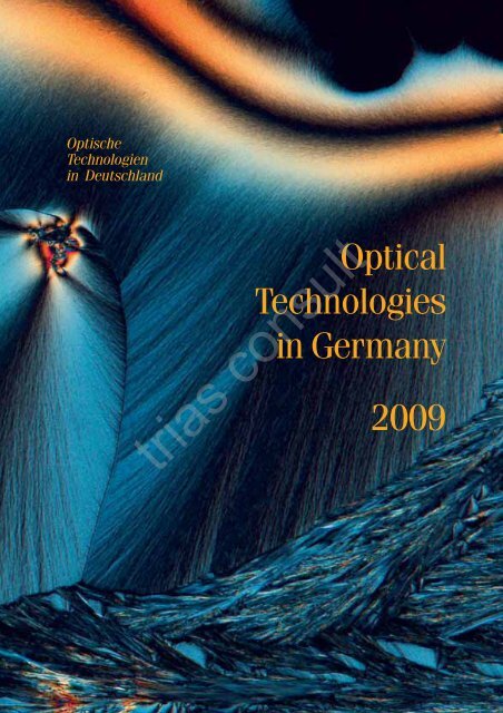
Optische<br />
Technologien<br />
in Deutschland<br />
Optical<br />
Technologies<br />
in Germany<br />
<strong>trias</strong> <strong>consult</strong><br />
2009
Impressum<br />
Publisher /Herausgeber<br />
<strong>trias</strong> Consult<br />
Johannes Lüders<br />
Crellestraße 31<br />
D – 10827 Berlin<br />
Phone +49 (0)30-781 11 52<br />
Mail <strong>trias</strong>-<strong>consult</strong>@gmx.de<br />
Web Optical-Technologies-in-Germany.de<br />
Translation/Übersetzung<br />
Dr. Otto-G. Richter<br />
Richter IT & Science Consulting<br />
Costa Mesa, CA, USA<br />
Mail otto@rits-<strong>consult</strong>ing.us<br />
otto@richter-its-<strong>consult</strong>ing.de<br />
Layout<br />
Uta Eickworth, Berlin<br />
eickworth@onlinehome.de<br />
Printing/ Druck<br />
GCC Grafisches Centrum Cuno, Calbe<br />
2009, Printed in Germany<br />
Nanogenaue Kraftzwerge<br />
NEXACT ® – Schrittantriebe mit großen Stellwegen vereinen Sub-<br />
Nanometerauflösung und gute Dynamik mit sehr kompakten Abmessungen.<br />
■ Auflösung < 100 Picometer ■ 25 x 25 x 8 mm klein<br />
■ Geschwindigkeit 10 mm/s ■ unbegrenzter Stellweg<br />
■ Antriebskraft 10 N<br />
■ vakuumtauglich<br />
Erfahren Sie mehr über unsere Kraftzwerge unter: info@pi.ws<br />
Physik Instrumente (PI) GmbH & Co.KG · Tel. 07214846-0 · www.pi.ws<br />
Photo Credits/Bildnachweis<br />
Title Photo/Titelfoto<br />
Frank Brückner, Berlin:<br />
Ascorbic acid in shifted, polarized light<br />
Ascorbinsäure im verschobenen polarisierten Licht<br />
Page/Seite<br />
S 3 <strong>Max</strong>-<strong>Born</strong>-<strong>Institut</strong> <strong>für</strong> Nichtlineare Optik<br />
und Kurzzeitspektroskopie/Forschungsverbund<br />
Berlin e. V.<br />
S 10/11 Leibinger Stiftung<br />
S 36/37 JENOPTIK AG<br />
S 49 PolyIC GmbH & Co KG<br />
S 66/67 Jürgen Berger, <strong>Max</strong> Planck <strong>Institut</strong> <strong>für</strong><br />
Entwicklungsbiologie<br />
S 77 SCHOTT AG<br />
<strong>trias</strong> <strong>consult</strong>
TABLE OF CONTENTS<br />
INHALTSVERZEICHNIS<br />
4 5<br />
Table of Contents<br />
Welcoming Addresses<br />
Grußworte<br />
6 Prof. Dr. Annette Schavan<br />
Federal Minister for Education and Research<br />
Bun<strong>des</strong>ministerin <strong>für</strong> Bildung und Forschung<br />
8 Dr. Dieter Kurz<br />
Research Union Economy-Science,<br />
CEO Carl Zeiss AG;<br />
Forschungsunion Wirtschaft-Wissenschaft,<br />
Vorsitzender <strong>des</strong> Konzernvorstands der<br />
Carl Zeiss AG<br />
Current Solutions and New Dimensions<br />
in Optical Technologies<br />
Aktuelle Lösungen und neue Dimensionen<br />
in den Optischen Technologien<br />
12 Theodor Hänsch et al.,<br />
<strong>Max</strong>-Planck-<strong>Institut</strong>e of Quantum Optics:<br />
“First light” for Frequency Combs to Enable<br />
Cosmic Dynamics Experiments<br />
14 Jürgen Popp,<br />
University of Jena:<br />
Luminous Visions for Better Health Care:<br />
The Biophotonics Research Program<br />
16 Stephan Sigrist,<br />
Charité University Medical Center, Berlin:<br />
Why Are We Interested in Flies that Turn<br />
into Crash Pilots?<br />
Looking at proteins in nerve cells with<br />
the STED microscope<br />
Warum interessieren uns Fliegen, die zu<br />
Bruchpiloten werden?<br />
Mit dem STED-Mikroskop Proteine in<br />
Nervenzellen beobachten<br />
18 Michael Heckmeier,<br />
Merck KG a A:<br />
Status and Future of Organic Electronics<br />
20 Jörg Amelung,<br />
Fraunhofer IMPS:<br />
Flat Light Sources on the Basis of Organic<br />
Light-Emitting Dio<strong>des</strong> – A new technology<br />
for the lighting of the future<br />
22 Andreas Tünnermann and Jacques Duparré,<br />
Fraunhofer IOF:<br />
Micro- and Nanooptics: New Prospects<br />
in Optical Technologies<br />
24 Henning Schröder,<br />
Fraunhofer IZM:<br />
New Optical Interconnects for Communication<br />
and Sensors<br />
26 Peter Leibinger,<br />
Trumpf GmbH + Co. KG:<br />
Precision Work in Metal: Optical sensors for<br />
material processing with lasers<br />
28 Jürgen Czarske, Lars Büttner, Thorsten Pfister,<br />
Technical University of Dresden:<br />
The Laser Doppler Distance Sensor<br />
30 Richard Hendel,<br />
ROFIN Baasel Lasertechnik GmbH & Co.KG:<br />
Solar Cells with Enhanced Efficiency Due to Laser<br />
Processing; Effizientere Solarzellen mit dem Laser<br />
32 Wilfried Bauer,<br />
Polytec GmbH:<br />
White Light Interferometry for Quality Control<br />
of Functional Surfaces<br />
34 Ronald Holzwarth and Michael Mei,<br />
Menlo Systems GmbH:<br />
Not Just Fast – Ultrafast: Femtosecond fiber<br />
lasers as enabling tools<br />
Markets and Networks in Germany<br />
Marktplätze und Netzwerke in<br />
Deutschland<br />
38 Messe München International:<br />
LASER World of PHOTONICS, World of Photonics<br />
Congress<br />
40 SPECTARIS e. V<br />
42 OptecNet Deutschland e. V.<br />
44 Deutsche Gesellschaft <strong>für</strong> angewandte<br />
Optik e. V., DGaO<br />
46 TSB Innovationsagentur Berlin GmbH<br />
The Congress Laser-Optics<br />
Berlin 2008<br />
Der Kongress Laser-Optics<br />
Berlin 2008<br />
50 TSB Adlershof:<br />
Laser Optics Berlin – showcase of the region<br />
Laser Optics Berlin – Schaufenster der Region<br />
52 Ursula Keller,<br />
ETH Zurich:<br />
Advancing Frontiers: Ultrafast Lasers Enable New<br />
Applications<br />
54 Philip Russell,<br />
<strong>Max</strong>-Planck Research Group,<br />
University of Erlangen-Nuremberg:<br />
Photonic Crystal Fibers: Light in a Tight<br />
Space<br />
56 Rüdiger Grunwald et al.,<br />
<strong>Max</strong> <strong>Born</strong> <strong>Institut</strong>e for Nonlinear Optics and<br />
Short-Pulse Spectroscopy:<br />
Ultrashort-Pulse Transfer Functions of Spatial<br />
Light Modulators<br />
58 Harald R. Telle,<br />
Physikalisch-Technische Bun<strong>des</strong>anstalt:<br />
Femtosecond Lasers as Metrological Tools<br />
60 Jürgen Petter et al.,<br />
Luphos GmbH:<br />
Ultra High Precision Non-Contact Distance<br />
Measurement using Multi Wavelength<br />
Inter ferometry<br />
62 Günter Rinke et al.,<br />
Forschungszentrum Karlsruhe:<br />
Raman-Spectroscopy for Measuring Concentration<br />
Profiles within Micro Channels<br />
64 Hans-Gerd Löhmannsröben,<br />
University of Potsdam:<br />
Micro-O 2 -Lasersensor and Laser Ion Mobility<br />
Spectrometry – Two Optical Techniques for the<br />
Detection of Chemical Substances<br />
Results and Services from<br />
Research <strong>Institut</strong>ions<br />
Ergebnisse und Leistungen<br />
in Forschungseinrichtungen<br />
<strong>trias</strong> <strong>consult</strong><br />
68 Fraunhofer IOF:<br />
Tailored Light – Licht nach Maß<br />
70 <strong>Institut</strong>e of Photonic Technology:<br />
Research and Development at the IPHT<br />
72 Fraunhofer IPM:<br />
Optical High Speed Systems – Reliable even<br />
in rugged environments<br />
73 Fraunhofer IAP:<br />
Novel Polymer Systems for Optical Technologies<br />
Neuartige Polymersysteme <strong>für</strong> optische<br />
Technologien<br />
74 Fraunhofer IWS:<br />
Mirrors for X-rays and EUV Radiation<br />
Spiegeloptiken <strong>für</strong> Röntgen- und<br />
EUV-Strahlung<br />
76 innoFSPEC Potsdam:<br />
From Molecules to Galaxies<br />
Inhaltsverzeichnis<br />
Innovations and Competencies<br />
in Industry<br />
Innovationen und Kompetenzen<br />
aus Unternehmen<br />
78 LightTrans GmbH<br />
79 JENOPTIK AG<br />
80 LT Ultra-Precision Technology GmbH<br />
81 MICOS GmbH<br />
Laser Technology<br />
Lasertechnik<br />
82 LASOS Laser, Service und optische<br />
Systeme GmbH<br />
83 LIMO Lissotschenko Mikrooptik GmbH<br />
84 Omicron Laserage Laserprodukte GmbH<br />
85 RAYLASE AG<br />
86 Scansonic GmbH<br />
87 TOPTICA Photonics AG<br />
Precision Manufacture<br />
and its Protection<br />
Präzisionsfertigung<br />
und deren Sicherung<br />
88 AudioDev GmbH Thin Film Metrology<br />
89 Micro-Hybrid Electronic GmbH<br />
90 TRIOPTICS GmbH<br />
91 ZygoLOT GmbH<br />
Systems, Components, and<br />
Intermediate Products of<br />
Optics<br />
Systeme, Komponenten und<br />
Vorprodukte der Optik<br />
92 II-VI Deutschland GmbH<br />
93 BERLINER GLAS KGaA<br />
Herbert Kubatz GmbH & Co.<br />
94 Leybold Optics GmbH<br />
96 LEONI Fiber Optics GmbH<br />
98 FiberTech GmbH<br />
99 OHARA GmbH<br />
100 LINOS Photonics GmbH & Co. KG<br />
102 Qioptiq GmbH<br />
103 OWIS GmbH<br />
104 Physik Instrumente (PI)<br />
GmbH & Co. KG<br />
105 piezosystem jena GmbH<br />
106 Sypro Optics GmbH<br />
108 u2t Photonics AG<br />
110 Schott AG
6 7<br />
Preface<br />
Optical technologies are among the most important key<br />
technologies in Germany. They set the pace for innovations<br />
and have in recent years also become a remarkable<br />
economic factor. Today, both lighting technology and power<br />
engineering would be unthinkable without optical technologies.<br />
The OLED initiative, which was launched in 2006 under<br />
the “Optical Technologies” funding programme and will run<br />
until 2011, has the aim of encouraging progress in the field<br />
of organic light-emitting dio<strong>des</strong>. Conventional light bulbs<br />
should soon be replaced by environmentally friendly alternatives,<br />
which, in laboratories, already produce a ten times<br />
higher light output. Strong research alliances between science<br />
and industry can enable forward-looking new lighting<br />
concepts. By developing resource-saving products, these<br />
alliances can open up new market opportunities worth billions<br />
of euros. The success of the OLED initiative within the<br />
High-Tech Strategy clearly shows that by forming innovation<br />
alliances, science and industry can set the course for the<br />
future. For every euro that the Federal Ministry of Education<br />
and Research invests in this innovation alliance, the private<br />
sector adds a further five euros.<br />
Prof. Dr. Annette Schavan,<br />
Federal Minister of Education<br />
and Research<br />
Bun<strong>des</strong>ministerin <strong>für</strong> Bildung<br />
und Forschung<br />
Germany is the “Land of Light”. In 2007, a project on semiconductor<br />
lighting received the Federal President’s Award<br />
for Technology and Innovation. This and many other awards<br />
show that our research funding policy takes the right approach<br />
and that German technology also sets international<br />
standards.<br />
But in addition to supporting research, the support of<br />
young scientists in the field of optical technologies will<br />
also be also decisive for our future. With “Luka’s Land<br />
of Research“, an initiative for kindergartens and primary<br />
schools, the “Innovation League” for older pupils, and new<br />
degree courses such as the Master’s degree programmes<br />
in photonics in Jena and Karlsruhe, we have already gone<br />
some way towards achieving this aim. We want to continue<br />
on this path and ensure that Germany makes better use of<br />
the great potential offered by optical technologies.<br />
Prof. Dr Annette Schavan, MdB<br />
Federal Minister of Education and Research<br />
Die optischen Technologien gehören in Deutschland zu den<br />
zentralen Schlüsseltechnologien. Sie sind Schrittmacher <strong>für</strong><br />
Innovationen und wurden in den vergangenen Jahren zu<br />
einem beeindruckenden Wirtschaftsfaktor. Weder aus der<br />
Beleuchtungs- noch aus der Energietechnik sind optische<br />
Technologien heute wegzudenken.<br />
Mit der OLED-Initiative, die 2006 im Rahmen <strong>des</strong> Förderprogramms<br />
„Optische Technologien“ gestartet ist, wollen<br />
wir bis 2011 die Forschung auf dem Gebiet der organischen<br />
Leuchtdioden vorantreiben. Die herkömmliche Glühbirne<br />
soll schon bald von umweltfreundlichen Alternativen abgelöst<br />
werden, die bereits jetzt in Laboren das Zehnfache an<br />
Lichtausbeute erreichen. Kompetenzstarke Forschungsverbünde<br />
aus Wissenschaft und Industrie ermöglichen Beleuchtungskonzepte<br />
<strong>für</strong> morgen.<br />
Und sie eröffnen sich durch ressourcenschonende Produkte<br />
Marktchancen in Milliardenhöhe. Der Erfolg der OLED-<br />
Initiative im Rahmen der Hightech-Strategie zeigt deutlich:<br />
Wenn Wissenschaft und Wirtschaft Innovationsallianzen eingehen,<br />
werden Weichen <strong>für</strong> die Zukunft gestellt. Für jeden<br />
vom Bun<strong>des</strong>ministerium <strong>für</strong> Bildung und Forschung in dieser<br />
Innovationsallianz eingesetzten Euro investiert die Wirtschaft<br />
weitere fünf Euro.<br />
<strong>trias</strong> <strong>consult</strong><br />
Deutschland ist das „Land <strong>des</strong> Lichts“. 2007 wurde ein Projekt<br />
zur Halbleiterbeleuchtung mit dem Zukunftspreis <strong>des</strong><br />
Bun<strong>des</strong>präsidenten ausgezeichnet. Diese Auszeichnung und<br />
viele weitere Preise zeigen, dass unsere Forschungsförderung<br />
in die richtige Richtung weist und die deutsche Technologie<br />
auch international Maßstäbe setzt.<br />
Doch nicht nur die Unterstützung der Forschung, auch die<br />
Förderung <strong>des</strong> Nachwuchses im Bereich der optischen Technologien<br />
entscheidet über unsere Zukunft.<br />
Mit dem „Lukas Forscherland“, einer Initiative <strong>für</strong> Kindergärten<br />
und Grundschulen, mit der „Innovationsliga“ <strong>für</strong> die<br />
älteren Schüler sowie neuen Studiengängen wie dem Photonics-Masterstudiengang<br />
in Jena und Karlsruhe konnten wir<br />
wichtige Akzente in der Nachwuchsförderung setzen. Diesen<br />
Weg wollen wir weitergeben, um die Chancen der optischen<br />
Technologien in Deutschland noch besser zu nutzen.<br />
Prof. Dr. Annette Schavan, MdB<br />
Bun<strong>des</strong>ministerin <strong>für</strong> Bildung und Forschung<br />
Grußwort
8 9<br />
Preface Grußwort<br />
Optical technologies represent one of Germany's greatest<br />
strengths in its role as a major production and investment<br />
location. They have therefore been included in the German<br />
government's high-tech strategy as one of the key areas to<br />
be pursued in the future. At the same time, harnessing light<br />
is a technology that has a broad and far-reaching impact<br />
on other areas.<br />
Nevertheless, the possibilities that light offers as a universal<br />
tool have only just begun to be unraveled, and optical<br />
technologies still have a huge, unexploited potential. Efforts<br />
are being made within industry and in the scientific<br />
community to unearth this potential and to gradually make<br />
it more accessible. This work is based on the wide variety<br />
of extraordinary properties that light encompasses, ranging<br />
from top-notch precision and maximum velocity to extremely<br />
short pulse durations and top-class optical power.<br />
Optical technologies take advantage of all these different<br />
properties.<br />
Germany is perfectly positioned in the field of optical technologies.<br />
It accommodates both highly-competitive, major<br />
global companies and key user industries, while around<br />
100,000 people are employed by the companies from<br />
the optical industry sector as well as their suppliers. The<br />
strength of innovation in this industry is highlighted by the<br />
fact that its research and development expenditure comes<br />
to approximately 9.5% of turnover. The intermeshing of the<br />
industry with cutting-edge research and world-renowned<br />
centers of expertise has created a highly successful network.<br />
So it is hardly surprising to find German companies occupying<br />
leading positions in some key areas of application. In<br />
optical lithography, where ultra-precision lenses are used<br />
Dr. Dieter Kurz,<br />
Research Union<br />
Economy-Science,<br />
CEO Carl Zeiss AG<br />
Forschungsunion<br />
Wirtschaft-Wissenschaft<br />
Vorsitzender <strong>des</strong><br />
Konzernvorstands<br />
der Carl Zeiss AG<br />
to produce semiconductor chips, German optics are the<br />
leading the market. The laser systems used in materials<br />
processing are another example, with a quarter of all the<br />
systems sold worldwide having been made in Germany.<br />
In addition to their technical applications, the advantages<br />
of optical technologies are also put to good use in the<br />
medical technology and life science arenas. Nowadays, it<br />
is hard to imagine a clinical environment without surgical<br />
microscopes for microsurgery, endoscopes, laser diagnosis<br />
and laser treatment. Meanwhile, research is focusing<br />
on systems such as laser scanning and fluorescence microscopes,<br />
which aim to discover more about cell processes.<br />
Optical technologies can also be found in everyday appliances:<br />
LED lights represent an efficient and environmentally-sound<br />
alternative that promises to provide significant<br />
cuts in CO 2 emissions and energy costs if adopted on a<br />
broad scale.<br />
Germany really is an excellent location for optical technologies,<br />
with superb scientific foundations, highly-competitive<br />
companies, and a whole host of people who are striving to<br />
move this richly traditional industry into the future with their<br />
enthusiasm for innovation and a will to succeed.<br />
Dr. Dieter Kurz<br />
Research Union Economy-Science<br />
Optische Technologien sind eine der herausragenden Stärken<br />
<strong>des</strong> Standorts Deutschland. Sie zählen daher auch zu<br />
den Zukunftsfeldern der Hightech-Strategie der Bun<strong>des</strong>regierung.<br />
Gleichzeitig ist das Beherrschen von Licht eine Querschnittstechnologie<br />
mit großer Breitenwirkung.<br />
Dabei steht Licht als universelles Werkzeug erst am Anfang<br />
seiner Möglichkeiten. Denn in den Optischen Technologien<br />
liegt noch ein großes, unausgeschöpftes Potenzial. Wissenschaft<br />
und Industrie arbeiten daran, diese Möglichkeiten<br />
auszuloten und Schritt <strong>für</strong> Schritt nutzbar zu machen. Sie<br />
setzen dabei auf die Vielzahl von außergewöhnlichen Eigenschaften,<br />
die Licht in sich vereint: Sei es höchste Präzision,<br />
maximale Geschwindigkeit, kürzeste Pulsdauer oder höchste<br />
Leistung. All diese Eigenschaften machen sich die Optischen<br />
Technologien zunutze.<br />
<strong>trias</strong> <strong>consult</strong><br />
Deutschland ist auf dem Gebiet der Optischen Technologien<br />
sehr gut aufgestellt. International führende und wettbewerbsfähige<br />
Unternehmen sind hier ebenso zuhause wie<br />
bedeutende Anwenderbranchen. In den Unternehmen der<br />
Optischen Industrie und bei ihren Zulieferern arbeiten rund<br />
100 000 Beschäftigte. Forschungs- und Entwicklungsaufwendungen<br />
in Höhe von rund 9,5 Prozent <strong>des</strong> Umsatzes<br />
belegen die innovative Kraft der Branche. Gemeinsam mit<br />
der Industrie bilden Spitzenforschung und Kompetenzzentren<br />
mit Weltgeltung zusammen ein erfolgreiches Netzwerk.<br />
Es ist daher kein Wunder, dass deutsche Unternehmen in<br />
wichtigen Anwendungsfeldern eine führende Position einnehmen:<br />
In der Optischen Lithographie, also bei den Objektiven<br />
<strong>für</strong> die Fertigung von Halbleiterchips, sind Optiken aus<br />
Deutschland Marktführer. Ein anderes Beispiel sind Lasersysteme<br />
<strong>für</strong> die Materialbearbeitung, bei welchen weltweit<br />
je<strong>des</strong> vierte die Marke „made in Germany“ trägt.<br />
Neben den technischen Anwendungen profitieren auch die<br />
Medizintechnik und die Biowissenschaften von den Möglichkeiten<br />
der Optischen Technologien. Operationsmikroskope<br />
<strong>für</strong> die Mikrochirurgie, Endoskope oder die Laserdiagnose<br />
und -behandlung sind heute aus dem klinischen Alltag nicht<br />
mehr wegzudenken. Die Forschung setzt auf Systeme wie<br />
Laserscan- und Fluoreszenzmikroskope, um mehr über Zellprozesse<br />
zu erfahren.<br />
Optische Technologie steckt auch in Geräten <strong>für</strong> den Alltag.<br />
LED-Leuchten bieten sich als effiziente und umweltverträgliche<br />
Alternativen an, die bei breiter Anwendung erhebliche<br />
Einsparungen beim CO 2-Ausstoß und bei den Energiekosten<br />
versprechen.<br />
Als Standort <strong>für</strong> Optische Technologien hat Deutschland die<br />
besten Voraussetzungen: Eine exzellente wissenschaftliche<br />
Basis, leistungsfähige Unternehmen und die Menschen, die<br />
mit Freude am Erfolg und mit Begeisterung <strong>für</strong> die Innovation<br />
diese traditionsreiche Branche auf die Zukunft ausrichten.<br />
Dr. Dieter Kurz<br />
Forschungsunion Wirtschaft-Wissenschaft
Current Solutions<br />
and New Dimensions<br />
in Optical Technologies<br />
<strong>trias</strong> <strong>consult</strong><br />
Aktuelle Lösungen<br />
und neue Dimensionen<br />
in den Optischen Technologien
12<br />
“First light” for Frequency<br />
Combs to Enable Cosmic<br />
Dynamics Experiments<br />
CURRENT SOLUTIONS AND NEW DIMENSIONS IN OPTICAL TECHNOLOGIES<br />
Tilo Steinmetz, Thomas Udem, Ronald Holzwarth, Tobias Wilken,<br />
Theodor Hänsch, <strong>Max</strong>-Planck-<strong>Institut</strong> <strong>für</strong> Quantenoptik;<br />
Michael Mei, Menlo Systems GmbH<br />
Recent cosmological observations suggest that the universe’s<br />
expansion is accelerating. Several lines of evidence<br />
corroborate this, including results from distant supernovae,<br />
the cosmic microwave background, and the clustering of<br />
matter. In the following we outline a new method based on<br />
direct frequency measurements of the cosmological redshifts.<br />
We have applied so called Optical Frequency Combs<br />
for the calibration of a traditional spectrograph in order to<br />
explore deep space more accurate than anybody before.<br />
The Optical Frequency Comb with its extremely regular<br />
spacing of individual frequency lines has proven to be a<br />
powerful tool for optical frequency metrology (1, 2). Each<br />
mode is phase coherently stabilized relative to the repetition<br />
rate controlled by an atomic clock. This allows to transfer<br />
the accuracy of the atomic clock in a single step to the<br />
optical domain. It provi<strong>des</strong> the means to perform absolute<br />
optical frequency measurements with the accuracy of the<br />
most accurate device that exists.<br />
We demonstrate the use of frequency combs to calibrate<br />
traditional spectrographs for a direct measurement of the<br />
universe’s expansion history by observing in real time the<br />
evolution of the cosmological redshift of distant objects<br />
(3). Here, the frequency comb acts as a transfer device<br />
Figure 1: An<br />
artistic view of<br />
the experiment:<br />
a spectrograph<br />
for measuring<br />
the universe<br />
expansion is illuminated<br />
with<br />
the precise lines<br />
of a frequency<br />
comb.<br />
Prof. Dr. Theodor<br />
W. Hänsch,<br />
winner of the Nobel Prize<br />
for Physics in 2005<br />
that allows to map an incoherent light source, otherwise<br />
not accessible with coherent counting techniques, to the<br />
phase controlled mo<strong>des</strong> of a frequency comb.<br />
Traditional spectral calibration techniques use a crowd of<br />
emission or absorption lines, for example from a Thorium-<br />
Argon-lamp, at known laboratory wavelengths as reference<br />
to map the detector pixels into wavelengths. However, calibration<br />
units are subject to uncertainties that unavoidably<br />
degrade the wavelength solution: Lines are not evenly dis-<br />
Figure 2: Basic scheme of a laser frequency comb. A modelocked<br />
laser creates femtosecond pulses at hundreds of megahertz<br />
frequencies, frep (top), that are synchronized with an atomic<br />
clock. A spectrum of the pulses (bottom) is composed of many<br />
mo<strong>des</strong> that are uniformly spaced in wavelength (or frequency)<br />
and cover a spectral bandwidth given roughly by the inverse of<br />
the pulse duration.<br />
Each mode’s wavelength (or frequency) does not have to be<br />
measured, but instead is given by a mathematical relation that<br />
inclu<strong>des</strong> frep, known a priori with very high accuracy. Laser<br />
frequency combs could therefore become the perfect wavelength<br />
calibration technique for astrophysical experiments that require<br />
high accuracy and long-term stability.<br />
AKTUELLE LÖSUNGEN UND NEUE DIMENSIONEN IN DEN OPTISCHEN TECHNOLOGIEN<br />
tributed in the spectral range of interest, have a wide range<br />
of intensities, and sometimes appear blended. These systematic<br />
effects limit the capabilities of current high-resolution<br />
spectrometers and hinder experiment repeatability,<br />
crucial for any long-term monitoring.<br />
The laser frequency combs (4, 5) may offer a solution.<br />
Because time – and thus frequency – is the most accurately<br />
measured quantity in physics thanks to atomic clocks, each<br />
mode’s frequency (or wavelength) is accurately known a<br />
priori and can be used as a perfect ruler to calibrate astronomical<br />
spectra.<br />
When the pulses pass through a spectrometer, a regular<br />
train of mo<strong>des</strong> is overlapped with the light collected by<br />
the spectrograph (see Figure 2) and hence can be used as<br />
the ideal tool for calibration of the system.<br />
Out of the approximately 500 000 available frequency<br />
lines from the comb we only just used a total of 58 lines<br />
in the first trial at the Vacuum Tower Telescope at Tenerife<br />
(see Figure 3). Although the telescope was not <strong>des</strong>igned for<br />
this purpose, we readily achieved a state-of-the-art calibration<br />
accuracy (5).<br />
We believe that using this technique with instruments<br />
specially <strong>des</strong>igned by the European Southern Observatory<br />
(ESO) such as the High Accuracy Radial velocity Planet<br />
Searcher (HARPS) will reduce calibration uncertainties by<br />
3 orders of magnitude. With this type of uncertainty, several<br />
intriguing observations will become possible. One of them<br />
is the detection of earth-like extra-solar planets orbiting<br />
sun-like stars from the recoil motion of the star (see Figure<br />
4). In addition, when monitoring the cosmic red shift<br />
for a few years, it will be possible to decide whether the<br />
expansion of the universe is accelerating. Such a direct observation<br />
could be decisive on whether or not dark energy,<br />
together with general relativity, constitute the proper model,<br />
or if we have to seek out for new explanations.<br />
In summary, we have shown that by combining our technique<br />
of optical frequency combs with some at-first-sight<br />
unrelated measurements of light from stars we can hope<br />
to explore the yet unknown.<br />
<strong>trias</strong> <strong>consult</strong><br />
1. T. Udem, R. Holzwarth, T. W. Hänsch, Nature 416, 233 (Mar 14,<br />
2002).<br />
2. T. Wilken, T. W. Hänsch, R. Holzwarth, P. Adel, M. Mei, paper presented<br />
at the Conference on Lasers and Electro-Optics (CLEO) 2007<br />
Baltimore, MD, USA, May 2007 2007.<br />
3. M. T. Murphy, T. Udem, R. Holzwarth, A. Sizmann, L. Pasquini, C.<br />
Araujo-Hauck, H. Dekker, S. D'Odorico, M. Fischer, T. W. Hänsch,<br />
A. Manescau, Monthly Notices of the Royal Astronomical Society<br />
(MNRAS) 380, 839 (2007).<br />
4. C.-H. Li, A. J. Benedick, P. Fendel, A. G. Glenday, F. X. Kärtner, D. F.<br />
Phillips, D. Sasselov, A. Szentgyorgyi, R. L. Walsworth, Nature 452,<br />
610 (2008).<br />
5. T. Steinmetz, T. Wilken, C. Araujo-Hauck, R. Holzwarth, T. W. Hänsch,<br />
L. Pasquini, A. Manescau, S. D’Odorico, M. T. Murphy, T. Kentischer,<br />
W. Schmidt, T. Udem, Science 321 (2008).<br />
6. For a more detailed <strong>des</strong>cription of the Frequency Comb FC1500 see<br />
www.menlosystems.com.<br />
Figure 3: A) The top left shows a scheme of the solar telescope<br />
(VTT) on Tenerife which has been used for the work in (5).<br />
The light from the Sun is superimposed with the Menlo Systems<br />
FC1500 frequency comb (6) by means of a beam splitter. Together<br />
they are fed to a spectrometer (upper right). Since the original<br />
mode separation of the frequency comb (250 MHz) is too close<br />
to be resolved by the spectrometer, the light is first filtered using<br />
an external Fabry-Pérot filter cavity to 15 GHz. B) A section of the<br />
measured spectrum, magnified on top. The dark lines are caused<br />
by absorption of gaseous elements in the photosphere of the Sun<br />
and by absorption in Earth's atmosphere. The spectral lines of the<br />
frequency comb appear as bright streaks that are used as precise<br />
calibration lines for the entire solar spectrum.<br />
Figure 4:<br />
Search of extrasolar planets<br />
by the reflex Doppler motion of<br />
their host stars.<br />
<strong>Max</strong>-Planck-<strong>Institut</strong> <strong>für</strong> Quantenoptik<br />
Prof. Dr. Theodor W. Hänsch<br />
Hans-Kopfermann-Str. 1<br />
D – 85748 Garching<br />
Phone + 49 (0)89 - 32905 - 712<br />
Fax + 49 (0)89 - 32905 - 312<br />
Mail t.w.haensch@mpq.mpg.de<br />
Web www.mpq.mpg.de<br />
13
14<br />
Luminous Visions for<br />
Better Health Care:<br />
The Biophotonics<br />
Research Program<br />
Optical methods have a long tradition in life sciences and<br />
medicine. Innovations like microscopy or the use of X-ray<br />
images for medical purposes allowed doctors and biologists<br />
insights into life processes. Today light based technologies<br />
contribute to further progress in this area. Like<br />
no other tool light is able to investigate cellular structures<br />
without doing harm. On the other hand, light can separate<br />
or even <strong>des</strong>troy cells in a much targeted way. Using these<br />
qualities to understand the causes of diseases and to treat<br />
them more individually is the major purpose of the Biophotonics<br />
Research Program which has been supported by<br />
the German Federal Ministry of Education and Research<br />
(BMBF) since 2002. Currently 14 network projects bringing<br />
together science and economy are working on optical solutions<br />
for biological and medical applications.<br />
Since the Biophotonics Research Program started an<br />
emphasis has been put on the early diagnosis of cancer.<br />
The earlier cancer can be detected the higher are the<br />
chances to be cured. This is where the network project<br />
“TumorVision“ sets in. It aims at detecting the first alterations<br />
of cells towards malignant tumors. Two molecules<br />
that are enzymatically active and mainly produced in tumor<br />
cells serve as markers there. Together scientists and<br />
physicians are working on a fluorescence endoscope that<br />
makes those markers – and with them malignant tumors<br />
– visible.<br />
The bioaerosol monitor MICROBUS delivers efficient pollen counts<br />
CURRENT SOLUTIONS AND NEW DIMENSIONS IN OPTICAL TECHNOLOGIES<br />
Prof. Dr. Jürgen Popp,<br />
Speaker Research<br />
Framework<br />
»Biophotonics«<br />
The “LUNA” project investigates a new contrast medium<br />
for early cancer diagnosis and therefore explores the<br />
application of novel fluorescent nano crystals in diagnostic<br />
imaging. The crystals are supposed to accrete to proteins<br />
which are changed due to the disease. This way they can<br />
give evidence of such proteins in tissues.<br />
The project “Exprimage”, as another example, tries to<br />
improve the prognosis of the course of cancer via multimodal<br />
imaging. For that different methods like digital microscopy,<br />
automated image analysis, biomolecular analysis,<br />
optical elasticity testing of cells or vibration spectroscopy<br />
are combined. As a result, the patient can be treated in a<br />
more individualized and efficient way.<br />
Furthermore, optical technologies offer new approaches<br />
in understanding certain skin diseases. White cancer,<br />
for instance, has been an underestimated disease so far<br />
because its skin mutations are often not recognized by the<br />
patient. The project “FluoTOM“ investigates a diagnostic<br />
system doing without artificial markers, surgery or radiological<br />
contamination. The physician immediately receives<br />
diagnostic cross sections of the tissue volume allowing<br />
the assessment of a tumour’s expansion, position or aggressiveness.<br />
Another project deals with neurodermatitis whose complex<br />
causes are still relatively unknown. The five-dimensional<br />
intravital tomograph of the project “5D IVT” might change<br />
this soon. The tomograph depicts dynamic processes in<br />
the skin even in deeper layers without adding a contrast<br />
medium or taking a sample. For the first time processes<br />
like the distribution of active agents can be observed<br />
precisely. Technically 5D-IVT combines three-dimensional<br />
multiphoton fluorescence imaging with spectral and time<br />
resolved detection methods.<br />
That the concept standing behind the Biophotonics<br />
Research Program is a successful one becomes visible<br />
already. Two of the earlier network projects have been able<br />
to introduce marketable appliances by now: When it comes<br />
to the identification of bacteria in the air, water or soil, a<br />
fast result is necessary. So far the cultivation of bacteria<br />
has taken several days. This is why the researchers within<br />
the “OMIB” project have developed an in-situ monitor which<br />
is able to recognize an unknown bacterium within a second.<br />
AKTUELLE LÖSUNGEN UND NEUE DIMENSIONEN IN DEN OPTISCHEN TECHNOLOGIEN<br />
The apparatus uses the fact that each molecule disperses<br />
incoming laser light in a specific way, and one gets a “molecular<br />
fingerprint” for each microbe. This is then evaluated<br />
via pattern recognition.<br />
The second project offering a finished product will bring<br />
great relief to many people: The bioaerosol monitor MICRO-<br />
BUS developed from the “OMNIBUSS” project and now<br />
delivers reliable and efficient pollen counts. MICROBUS is<br />
an automated pollen monitor which combines the microscopic<br />
evaluation of collected pollen with a complex pattern<br />
recognition system. This allows not only the recognition of<br />
the type of pollen but also its concentration in the air.<br />
But not only biogenic pollution of the air by bacteria or<br />
pollen causes problems, no less do fine particulates. That<br />
is why the current project “Monet” is working on an in-situ<br />
monitor measuring the percentage of fine particulates in<br />
the air in real time. The project “Optozell”, on the other<br />
hand, investigates microbiological contaminations of pure<br />
and drinking water. With the help of a quick-acting optosensory<br />
test system we will be able to immediately react on<br />
water pollution in the future.<br />
The leitmotif “light for health“ connects the different<br />
projects. We are searching for a deeper understanding of<br />
the causes of diseases which then is the key to an early<br />
recognition and targeted treatment – especially of cancer,<br />
infections and other wi<strong>des</strong>pread diseases. Even the economy<br />
can profit from biophotonics research because not<br />
only the patient benefits from a faster and more targeted<br />
treatment but also the health system. And it is extremely<br />
rewarding that the results of biophotonics research bring<br />
concrete improvements to patients and consumers within<br />
a relatively short period of time.<br />
<strong>trias</strong> <strong>consult</strong><br />
Prof. Dr. Jürgen Popp<br />
Spokesman Biophotonics Research Program<br />
<strong>Institut</strong>e of Physical Chemistry<br />
University of Jena<br />
Helmholtzweg 4<br />
07743 Jena<br />
Germany<br />
Phone +49 (0)3641-948-320<br />
Fax +49 (0)3641-948-302<br />
Mail juergen.popp@uni-jena.de<br />
Web www.biophotonik.org<br />
From left: Dr. Hans Eggers (BMBF, Department 513 "Optical<br />
Technologies“), Dr. Wolfram Eberbach (Thuringian Ministry of<br />
Education and Cultural Affairs), State Secretary Prof. Dr. Frieder<br />
Meyer-Krahmer (BMBF), Dr. Albrecht Schröter (Lord<br />
Mayor of Jena), Prof. Dr. Hans-J. Schwarzmaier (VDI Technology<br />
Center), Prof. Dr. Jürgen Popp (Spokesman Biophotonics<br />
Research Program), Dr. Hilmar Gugel (Leica Microsystems) at the<br />
biophotonics conference “Photonics meets LifeSciences” 2008<br />
in Jena.<br />
The Bio Particle Explorer of the project “OMIB”<br />
Luminescent nanoparticles are an important tool in biophotonics research<br />
Source: Forschungsschwerpunkt Biophotonik/Biophotonics Research<br />
Program Friedrich-Schiller-Universität Jena, <strong>Institut</strong> <strong>für</strong> Physikalische<br />
Chemie<br />
15
16<br />
CURRENT SOLUTIONS AND NEW DIMENSIONS IN OPTICAL TECHNOLOGIES<br />
Why Are We Interested in<br />
Flies that Turn into Crash Pilots?<br />
Looking at proteins<br />
in nerve cells with the<br />
STED microscope<br />
Prof. Dr. Stephan Sigrist, <strong>Institut</strong>e of Biology – Freie Universität<br />
Berlin, NeuroCluster of Excellence – Charité Berlin,<br />
answers a few questions on the application of super high<br />
resolution STED microscopy:<br />
Bruchpilot, which is German for crash pilot, is the name of<br />
one of the proteins you are researching. What does STED<br />
show you that you couldn’t see before?<br />
For the first time, STED brings light into darkness in this<br />
field. We recognize sub-structures of synapses and are able<br />
to localize proteins such as bruchpilot. Bruchpilot plays a<br />
key role in synaptic signal transmission in the nerve cells of<br />
the Drosophila fly by building up a specific structure there<br />
for supporting signal transmission. If the Drosophila fly<br />
does not have much bruchpilot, it cannot sustain flight, if it<br />
has none at all, it dies. The protein is found in similar form<br />
in humans, too, and could be connected with diseases of<br />
the nervous system. Studying animals helps to understand<br />
the functions of the protein in humans.<br />
Understanding biological signal transmission is not<br />
only important for science in general. It is probable that<br />
synaptic defects trigger a large number of neurodegenerative<br />
diseases. In addition, it is almost certain that memory<br />
and learning processes are organized at synapses.<br />
Immunohistological co-staining of two antibodies which<br />
bind at different regions of the synaptic protein Bruchpilot<br />
(BRP). The increased resolution resulting from the STED<br />
technology (green, BRP C-Term ) allows us to probe the spatial<br />
organization of BRP at synapses. The overlay of the sequentially<br />
acquired confocal images (red, BRP N-Term ) with the<br />
STED images clearly shows the higher resolution obtained<br />
by STED microscopy.<br />
Prof. Dr. Stephan Sigrist,<br />
<strong>Institut</strong> <strong>für</strong> Biologie –<br />
Freie Universität Berlin,<br />
NeuroCluster of Excellence –<br />
Charité Berlin<br />
Apart from its inventor, Prof. Stefan Hell, you were one of<br />
the first to work with STED. What was it like to see the<br />
first STED images?<br />
Without exaggerating, I can say that I discovered a new<br />
world. I immediately realized that STED is a breakthrough<br />
for finding answers to our questions and that we had had<br />
extremely naïve ideas of what we could see with light microscopy.<br />
But, after all, that’s the beauty of science – that<br />
new discoveries always raise new questions.<br />
Light microscopy is a key technology in life sciences. How<br />
important do you think STED will be in future?<br />
Very important indeed, as STED takes us into the realm of<br />
protein complexes and therefore gives us a really close up<br />
view of life. At present, we are able to resolve structures<br />
below the 100 nanometer mark.<br />
Professor Hell, who is working on the further development<br />
of STED, has already achieved far higher resolutions.<br />
If we can use resolutions of a few tens of nanometers, it<br />
will be possible to determine with light microscopy whether<br />
proteins are close together or further apart. This would<br />
constitute a further quantum leap in our understanding of<br />
protein functions.<br />
Prof. Sigrist was interviewed<br />
by Anja Schué, Leica Microsystems.<br />
Immunohistologische Ko-Färbung zweier Antikörper, die an unterschiedlichen<br />
Bereichen <strong>des</strong> synaptischen Proteins Bruchpilot<br />
(BRP) binden. Durch die verbesserte Auflösung der STED-Technologie<br />
(grün, BRP C-Term ) können Aussagen zur räumlichen Anordnung<br />
von BRP an der Synapse getroffen werden. Die Überlagerung<br />
der sequenziell aufgenommenen, konfokalen Bilder (rot, BRP N-<br />
Term ) mit den STED-Bildern verdeutlicht den Auflösungsgewinn<br />
durch die STED-Mikroskopie.<br />
AKTUELLE LÖSUNGEN UND NEUE DIMENSIONEN IN DEN OPTISCHEN TECHNOLOGIEN<br />
STED (Stimulated Emission Depletion) stands for a light microscopic<br />
technique in which resolution is no longer limited by the<br />
wavelength of the light. Its inventor, Prof. Dr. Stefan Hell of the<br />
<strong>Max</strong>-Planck-<strong>Institut</strong>e Göttingen, won the German Future Award<br />
2006. Leica Microsystems has an exclusive license to produce<br />
and market the STED Fluorescence Microscope Leica TCS STED.<br />
STED (Stimulated Emission Depletion) steht <strong>für</strong> ein lichtmikroskopisches<br />
Verfahren, bei dem die Auflösung nicht mehr durch<br />
die Lichtwellenlänge begrenzt ist. Erfinder Prof. Dr. Stefan Hell<br />
vom <strong>Max</strong>-Planck-<strong>Institut</strong> Göttingen erhielt da<strong>für</strong> den Deutschen<br />
Zukunftspreis 2006. Das STED-Fluoreszenzmikroskop Leica TCS<br />
STED wird von Leica Microsystems exklusiv in Lizenz produziert<br />
und vermarktet.<br />
Fragen an Prof. Dr. Stephan Sigrist, <strong>Institut</strong> <strong>für</strong> Biologie –<br />
Freie Universität Berlin, NeuroCluster of Excellence – Charité<br />
Berlin, zur Anwendung der super-hochauflösenden STED-<br />
Mikroskopie:<br />
<strong>trias</strong> <strong>consult</strong><br />
Bruchpilot – so heißt ein Protein, das Sie erforschen.<br />
Was sehen Sie mit STED, was vorher nicht möglich<br />
war?<br />
Mit STED können wir hier erstmals Licht ins Dunkle bringen.<br />
Wir erkennen Substrukturen der Synapsen und können<br />
Proteine wie Bruchpilot lokalisieren. Bruchpilot spielt eine<br />
zentrale Rolle bei der Signalübertragung in den Synapsen<br />
der Nervenzellen der Fruchtfliege, in dem es dort eine spezifische<br />
Struktur zur Unterstützung der Signalübertragung<br />
aufbaut. Hat die Fliege wenig Bruchpilot, stürzt sie ab, hat<br />
sie gar kein Bruchpilot, stirbt sie. Das Protein kommt in ähnlicher<br />
Form auch beim Menschen vor und könnte auch mit Erkrankungen<br />
<strong>des</strong> Nervensystems in Zusammenhang stehen.<br />
Tierstudien helfen, die Proteinfunktionen beim Menschen<br />
zu verstehen.<br />
Das Verständnis der biologischen Signalübertragung ist<br />
nicht nur aus Sicht der Grundlagenwissenschaft wichtig.<br />
Wahrscheinlich lösen synaptische Defekte viele neurode-<br />
Warum interessieren uns Fliegen,<br />
die zu Bruchpiloten werden?<br />
Mit dem STED-Mikroskop<br />
Proteine in Nervenzellen<br />
beobachten<br />
generative Erkrankungen aus. Zudem werden auch Erinnerungs-<br />
und Lernprozesse mit großer Sicherheit an Synapsen<br />
organisiert.<br />
Sie waren neben dem Erfinder Prof. Stefan Hell einer<br />
der Ersten, die mit STED gearbeitet haben. Wie war es,<br />
als Sie die ersten STED-Bilder gesehen haben?<br />
Mir hat sich – ohne zu übertreiben – eine neue Welt aufgetan.<br />
Ich habe sofort verstanden, dass STED <strong>für</strong> unsere Fragestellungen<br />
einen Durchbruch darstellt und dass wir sehr<br />
naive Vorstellungen von dem hatten, was wir mit konventioneller<br />
Lichtmikroskopie sehen konnten. Doch das Schöne<br />
an der Wissenschaft ist ja, dass neue Erkenntnisse immer<br />
wieder neue Fragen aufwerfen.<br />
Die Lichtmikroskopie ist eine zentrale Technologie in<br />
den Lebenswissenschaften. Wie schätzen Sie die Bedeutung<br />
von STED <strong>für</strong> die Zukunft ein?<br />
Ausgesprochen hoch, da wir mit STED in den Bereich von<br />
Proteinkomplexen vordringen und damit ganz nahe am Leben<br />
beobachten können. Zur Zeit können wir Strukturen unterhalb<br />
100 Nanometer auflösen. Professor Hell, der an der<br />
Weiterentwicklung von STED arbeitet, hat im Labor bereits<br />
weitaus höhere Auflösungen realisiert. Wenn wir Auflösungen<br />
von wenigen zehn Nanometern nutzen können, sind<br />
lichtmikroskopisch Aussagen darüber möglich, ob Proteine<br />
nahe beieinander liegen oder weiter entfernt sind. Für das<br />
Verständnis der Proteinfunktionen wäre dies ein weiterer<br />
Quantensprung.<br />
Das Interview führte Anja Schué, Leica Microsystems.<br />
Leica Microsystems GmbH<br />
Frau Dr. Kirstin Henze<br />
Corporate Communications<br />
Ernst-Leitz-Straße 17 - 37<br />
D – 35578 Wetzlar<br />
Phone +49 (0)6441 - 29 - 2550<br />
Mail kirstin.henze@leica-microsystems.com<br />
Web www.leica-microsystems.com<br />
17
18<br />
Status and Future<br />
of Organic Electronics<br />
Organic Electronics is one of the key technologies of this<br />
century and Germany has in many segments a leading role.<br />
For this emerging industry, market research like IDTechEx<br />
is forecasting an overall market volume of 100 Bio US $<br />
in 2020. Recent investments and announcements of first<br />
movers seem to support such ambitious forecasts.<br />
A wide definition of Organic Electronics comprises OLED<br />
(Organic Light Emitting Dio<strong>des</strong>), OPV (Organic Photovoltaics),<br />
OTFT (Organic Thin Film Transistors) and others. They<br />
all have in common that the key active material that determines<br />
the device functionality is an organic semiconductor.<br />
Since OLED and OPV are covered by different articles in this<br />
issue, we focus in the following on OTFT only.<br />
Transistors are miniaturized electrical switches and<br />
are key elements in electronics and optics applications.<br />
Transistors, which today are based on silicon technology,<br />
are ubiquitous. In modern Liquid Crystal based televisions,<br />
every single pixel is switched by a TFT, integrated circuits<br />
including thousands of transistors are used in many modern<br />
devices for automotive, information, communication,<br />
consumer electronics, housing and other applications.<br />
The OTFT working principle<br />
For the sake of simplicity we exemplify the basic technical<br />
concept here for a field effect transistor. The unique features<br />
of an organic field effect transistor are in principle<br />
valid for other organic transistor types like bi-polar transis-<br />
Picture 1: Sketch of an organic Field Effect<br />
Transistor (O-FET).<br />
CURRENT SOLUTIONS AND NEW DIMENSIONS IN OPTICAL TECHNOLOGIES<br />
tors and for more complex electronics components based<br />
on organic materials.<br />
In an O-TFT instead of silicon an organic semiconductor<br />
is used (cp. Picture 1). These are highly conjugated small<br />
molecules or macromolecules based on many thousands<br />
of repeating molecular subunits. The source and drain electro<strong>des</strong><br />
are covered by the organic semiconductor. An insulating<br />
layer separates the organic semiconductor from the<br />
gate electrode. Based on the voltage applied to the gate<br />
electrode, the organic semiconductor changes its conductive<br />
properties from an insulator to a conductor, hence the<br />
gate voltage controls the current flowing between source<br />
and drain electrode.<br />
Key parameters that determine the performance and applicability<br />
of an O-TFT are the mobility of the charge carriers<br />
through the semiconductor layer and the process conditions<br />
that can be applied to the semiconductor. State of<br />
the art organic semiconductors achieve mobilities of more<br />
than 1 cm2/Vs. This is already in the range of charge carrier<br />
mobilites of amorphous silicon, which is widely used<br />
for transistors in liquid crystal based TVs.<br />
Referring to manufacturing process conditions, an important<br />
feature of these organic semiconductors is their<br />
solubility in organic solvents. This opens the door for all<br />
liquid based coating techniques to be used for the deposition<br />
of organic semiconductors. Important are printing<br />
Picture 2:<br />
Flexible<br />
display driven<br />
by an organic TFT array.<br />
Dr Michael Heckmeier, MBA<br />
Senior Director<br />
Advanced Technologies (AT-C)<br />
Merck Chemicals Ltd.<br />
Southampton, UK<br />
AKTUELLE LÖSUNGEN UND NEUE DIMENSIONEN IN DEN OPTISCHEN TECHNOLOGIEN<br />
Picture 3: Printable circuits on a roll-to-roll<br />
line. Source: PolyIC<br />
processes which can be applied to organic semiconductors<br />
and opens a new world compared to traditional semiconductors<br />
like silicon.<br />
Uniqueness of Organic Semiconductors and Organic<br />
Transistors<br />
The main advantage of organic semiconductors currently<br />
lies in the potential of much easier and faster processing<br />
compared to silicon based technologies. As solutions, the<br />
semiconductors can be printed, whole devices can be built<br />
up by printing layer by layer which is a fast and additive<br />
process that in principle can be done in ambient conditions<br />
without cleanroom facilities and with relative small<br />
plant investments. Printable formulations of organic semiconductors<br />
for established printing techniques like inkjet,<br />
gravure, flexographic or offset are available. This facilitates<br />
short production runs with roll-to-roll techniques on flexible<br />
substrates, opening the whole range of new flexible applications<br />
like flexible displays (picture 2), printable circuits<br />
(picture 3) or Radio Frequency Identification Tags (RFID),<br />
printable sensors and many others.<br />
<strong>trias</strong> <strong>consult</strong><br />
What are the key challenges ?<br />
Exhibiting a huge market potential, organic electronics<br />
still has to be considered as an emerging technology with<br />
many unknowns and hurdles to overcome. The complexity<br />
of bringing organic electronics to the market requires<br />
close cooperation along the whole value chain. Chemicals<br />
companies, printing companies, equipment, machinery and<br />
application and Universities and institutes have to work<br />
together to move the technology to mass production. Standards<br />
and specifications need to be developed, process<br />
parameters like printing registration are not defined yet and<br />
resolution for necessary system integration needs massive<br />
improvement.<br />
For the materials, key seems to be a strong interdependency<br />
between performance and process applicability, additionally<br />
more complex electrical circuit <strong>des</strong>igns require<br />
semiconductor mobilities of over 5 cm 2/Vs.<br />
There are many challenges ahead, but remarkable progress<br />
in the past years and a critical mass of players in<br />
the field will eventually pave the way for a bright future of<br />
organic electronics.<br />
Organic Electronics at Merck<br />
Merck is one of the industrial pioneers of organic electronics,<br />
starting own research and development about ten<br />
years ago. In 2005 Merck made a major acquisition in<br />
OLED materials, in 2006 Merck opened a laboratory for<br />
inorganic printable electronics together with the Technical<br />
University of Darmstadt. Since 2001 all OPV and O-TFT related<br />
activities of Merck are run in Merck’s Technical Centre<br />
in Southampton in the United Kingdom, which recently announced<br />
further investments to expand organic electronic<br />
research facilities. Merck’s organic electronics materials<br />
are commercialized under the brand name lisicon.<br />
Merck is one of the initiators of the OPV- BMBF initiative<br />
of the Federal Minister of Education and Research and<br />
will play a major role in the Spitzencluster initiative in the<br />
Innovation Laboratory in Heidelberg.<br />
Merck Chemicals Ltd.<br />
Chilworth Technical Centre,<br />
University Parkway,<br />
Southampton SO16 7QD, UK<br />
Phone +44 (0)23-8076-3310<br />
Fax +44 (0)23-8076-3380<br />
Mail michael.heckmeier@merckchem.co.uk<br />
Web http://www.merckchem.co.uk/<br />
19
20<br />
CURRENT SOLUTIONS AND NEW DIMENSIONS IN OPTICAL TECHNOLOGIES<br />
Flat Light Sources on the Basis<br />
of Organic Light-Emitting Dio<strong>des</strong><br />
A new technology for the lighting<br />
of the future<br />
Introduction<br />
The lamps predominantly used in today's general lighting<br />
engineering are incan<strong>des</strong>cent lamps and luminescent<br />
tubes, the production methods and functionality of which<br />
have been technologically mature for a long time. Add to<br />
this the light-emitting dio<strong>des</strong> (LED) made from semiconductors<br />
over the past decade their development has leapt<br />
forward. Due to their increased functionality, they are increasingly<br />
being used beyond their original service environment<br />
(indicator, status, signal lights, display technology) as<br />
light sources, too.<br />
In contrast to LEDs, lighting units based on organic<br />
light-emitting dio<strong>des</strong> (OLEDs) are still in a development<br />
stage, but they already show enormous potential as illuminants<br />
of the future. They will complement LEDs as a<br />
second, important solid-state illumination – a substantial<br />
growth market.<br />
Technical Background<br />
The electroluminescence on the basis of organic materials<br />
has been known for quite some time, but only in 1987<br />
could an efficient OLED be produced. In its simplest form,<br />
an OLED consists of stacks of organic layers (thickness<br />
about 100-200 nm), which are inserted between two electro<strong>des</strong><br />
(anode and cathode). Applied to a glass substrate,<br />
this area light source measures less than 2 mm in total.<br />
In applying a current, within the coating system light is<br />
produced which emanates through one of the electro<strong>des</strong>.<br />
Usually, the substrate is glass coated with a transparent<br />
conductive oxide being the anode, followed by the organic<br />
Demonstrator for Large-area OLED Lighting Applications<br />
stack, consisting of hole transport and electron transport<br />
materials, followed by the inorganic cathode. Key advantages<br />
of the organic luminescence are the chemical variability<br />
of the organic light-emitting dio<strong>des</strong>, allowing virtually<br />
any color including white, and the thin film system, allowing<br />
large-area and low-cost deposition, and the possibility to<br />
use thin and even flexible substrates to realize a novel<br />
class of lighting and display solutions not possible for other<br />
technologies.<br />
At present, two different systems of materials for organic<br />
light-emitting dio<strong>des</strong> are being researched: OLEDs<br />
based upon vacuum-coated small molecules, so-called<br />
small-molecules (SM-) OLEDs; and polymer light-emitting<br />
dio<strong>des</strong> (PLED) based upon polymers which are applied in<br />
the liquid phase. SM-OLEDs dominate the market; their<br />
share in the display field alone amounts to almost 100<br />
percent.<br />
Lighting on the basis of organic<br />
light-emitting dio<strong>des</strong>.<br />
The development of OLEDs triggered a rapid development<br />
which led to a consistent growth of the display industry,<br />
with a turnover of half a billion US $ in 2007. The main applications<br />
today are the small, so-called sub-displays, used<br />
for information in cell phones and MP3-players as well as<br />
in the first mini-format TVs.<br />
The efficiency of LEDs has increased to such a degree<br />
that in the case of green dio<strong>des</strong>, it exceeds that of inorganic<br />
light-emitting dio<strong>des</strong>. This has opened up yet another vast<br />
market of the future for OLEDs within large-area lighting.<br />
With their moderate luminance (as against LEDs), OLEDs<br />
are pre<strong>des</strong>tined for use in diffuse area light sources. Their<br />
low thickness makes novel, transparent as well as flexible<br />
illuminants a distinct possibility of the future.<br />
Already today, one thing seems for sure: light sources<br />
on the basis of organic light dio<strong>des</strong> will revolutionize the<br />
lighting market; replacing traditional lighting technology<br />
in the field of area light sources as a second solid light<br />
source besi<strong>des</strong> LEDs. First, large-quantity product series<br />
are predicted for as early as 2009. Marketing <strong>consult</strong>ing<br />
company IDTechEx Ltd. expects a market of 2.5 billion US $<br />
as early as 2010.<br />
AKTUELLE LÖSUNGEN UND NEUE DIMENSIONEN IN DEN OPTISCHEN TECHNOLOGIEN<br />
Jörg Amelung,<br />
Fraunhofer<br />
<strong>Institut</strong>e for<br />
Photonic<br />
Microsystems, Dresden<br />
Cluster tool for large-area OLED Deposition, Center for<br />
Organic Materials and Electronic Devices Dresden<br />
Center for Organic Materials and Electronic<br />
Devices Dresden - COMEDD<br />
Still, a few technical issues remain to be addressed. The efficiency<br />
of white OLEDs and their lifetime have to be further improved<br />
and translated into a cost-effective production. Several<br />
research institutes and companies are looking into solutions for<br />
these tasks. Together with the U.S.A. and Japan, Europe are in<br />
the vanguard of this development.<br />
However, for the European organic lighting industry to be influential<br />
in this market, it is a must that not only development<br />
and <strong>des</strong>ign, but also fabrication capacities are located here. In<br />
response to this, the Fraunhofer-Gesellschaft has founded the<br />
Center for Organic Materials and Electronic Devices Dresden<br />
(COMEDD). The new research center specializes in the development<br />
of cost-effective and production-ready processes for organic<br />
semiconductor devices such as OLEDs and organic solar cells<br />
on the one hand, and their integration into novel products on<br />
the other.<br />
The center's core facility are several vacuum coaters. For<br />
the production of OLEDs on glass substrates, a new production<br />
line for glass and foil was installed by Sunic System of South<br />
Korea in cooperation with Aixtron AG Germany. This line enables<br />
the prompt evaluation of new process concepts with a capacity<br />
of up to 13 000 m2 per year. For the development and production<br />
of flexible substrate OLED lighting module, COMEDD offers<br />
a roll-to-roll production line by Dresden company Von Ardenne<br />
Anlagentechnik GmbH installed at the Fraunhofer <strong>Institut</strong>e for<br />
Electron Beam and Plasma Technology – Fraunhofer FEP. Not only<br />
do the new coaters allow for the production of organic lighting<br />
systems. The research equipment also enables the production<br />
of organic solar cells on the basis of small molecules in a rollto-roll<br />
process. COMEDD belongs to the Fraunhofer <strong>Institut</strong>e for<br />
Photonic Microsystems (Fraunhofer IPMS) under its director, Professor<br />
Karl Leo.<br />
<strong>trias</strong> <strong>consult</strong><br />
Fraunhofer <strong>Institut</strong><br />
Photonische Mikrosysteme (IPMS)<br />
Jörg Amelung<br />
Maria-Reiche-Str. 2<br />
D – 01109 Dresden<br />
Phone +49 (0)351 - 8823 - 127<br />
Mail joerg.amelung@ipms.fraunhofer.de<br />
Web www.ipms.fraunhofer.de<br />
A scientist shows a large-area lighting unit fabricated in the<br />
Center for Organic Materials and Electronic Devices<br />
Flexible Organic Solar Cell<br />
21
22<br />
Micro- and Nanooptics:<br />
New P rospects in Optical<br />
Technologies<br />
Andreas Tünnermann and Jacques Duparré,<br />
Fraunhofer <strong>Institut</strong>e for Applied Optics<br />
and Precision Engineering IOF, Jena<br />
Optical technologies already have a long history in our life.<br />
Starting with the use of simple mirrors documented long<br />
before Christ over the invention of early microscopes and<br />
telescopes several hundred years ago optics mainly contributed<br />
to the understanding of our world. So e.g. Galileo<br />
Galilei used lens-telescopes for his observations about<br />
400 years ago and found mountains on the moon, sunspots,<br />
rings of Saturn and some moons of Jupiter.<br />
Today, the entirety of methods and procedures in the field<br />
of optics influences our way of life in an amount we couldn’t<br />
imagine a few deca<strong>des</strong> ago. However, the importance of<br />
light in our daily life will even further increase in the next<br />
years and in some cases it will even play a superior role.<br />
Optics consequently becomes an enabler and catalyst in<br />
science and engineering. Networks of glass fibres will support<br />
new forms of information and communication technologies.<br />
Minimal invasive therapies will take over more<br />
and more in the medical sciences, which potentially also<br />
will reduce costs in the health care system. Therefore the<br />
21st century is also called the century of light.<br />
The control of light in all its properties will play a major<br />
role in the dominant technologies of the next century. Here<br />
micro- and nanooptics have a special importance because<br />
they offer new possibilities to form novel optical systems<br />
and furthermore have compatibility within the meanwhile<br />
established semiconductor fabrication processes.<br />
CURRENT SOLUTIONS AND NEW DIMENSIONS IN OPTICAL TECHNOLOGIES<br />
Figure 1<br />
Drosophila<br />
Source:<br />
Jürgen Berger,<br />
<strong>Max</strong>-Planck-<strong>Institut</strong> <strong>für</strong><br />
Entwicklungs biologie,<br />
Tübingen<br />
Prominent examples for these novel types of optical systems<br />
are arrayed ultra-compact vision systems which have<br />
their archetypes in the eyes of invertebrates. Natural compound<br />
eyes combine small eye volumes with a large field<br />
of view, at the cost of comparatively low spatial resolution.<br />
For small invertebrates, as for instance flies or moths, the<br />
compound eyes are the perfectly adapted solution to obtain<br />
sufficient visual information about their environment<br />
without overloading their brain with the necessary image<br />
processing (Fig. 1).<br />
Nocturnal insects such as moths possess superposition<br />
compound eyes with high sensitivity and low resolution<br />
while diurnal insects such as flies show compound eyes of<br />
the apposition type which behave vice versa. All of theses<br />
eye forms can use refractive mechanisms for image formation<br />
while incorporating graded refractive index optics.<br />
In superposition compound eyes, reflective mechanisms<br />
can be found as well. A natural apposition compound eye<br />
consists of an array of micro-lenses on a curved surface<br />
(Fig. 2). Each micro-lens is associated with a small group<br />
of photo receptors in its focal plane. The single microlens<br />
receptor unit produces one image point for a certain<br />
direction in the overall compound eyes field of view and is<br />
commonly referred to as ”ommatidium”. Pigments form<br />
opaque walls between adjacent ommatidia to avoid light<br />
under a large angle which is focused by one micro-lens to<br />
Figure 2<br />
Diagram of a natural<br />
apposition compound<br />
eye (dragonfly);<br />
Facettenauge<br />
einer Libelle<br />
Source: public<br />
domain (previous:<br />
Meyers Konversationslexikon<br />
1888)<br />
(from Wikipedia))<br />
Prof. Dr. Andreas<br />
Tunnermann<br />
Dr. Jacques<br />
Duparré<br />
AKTUELLE LÖSUNGEN UND NEUE DIMENSIONEN IN DEN OPTISCHEN TECHNOLOGIEN<br />
Figure 3: Basic structure of an artificial apposition compound eye<br />
imaging optical sensor.<br />
be received by an adjacent channel’s receptor. Natural apposition<br />
compound eyes contain several hundreds (water<br />
fly) up to tens of thousands (honeybee or Japanese dragonfly)<br />
of these ommatidia packed in non-uniform hexagonal<br />
arrays. In superposition compound eyes several ommatidia<br />
contribute to the formation of one image point in order to<br />
increase the light sensitivity.<br />
A major challenge for a technical adoption of natural compound<br />
eyes is the required fabrication and assembly accuracy.<br />
Recent micro-optical fabrication technologies such<br />
as UV-replication allow for a highly precise generation of<br />
uniform micro-lens arrays with small lens sags and their<br />
accurate alignment to the subsequent optics-, spacingand<br />
optoelectronics structures. The results are ultra-thin<br />
monolithic imaging devices with the high accuracy of photo<br />
lithography for a variety of applications. However, up-todate<br />
artificial receptor arrays such as CCD- or CMOS image<br />
sensors are fabricated on planar wafers. Thus, a thin<br />
monolithic objective based on the artificial compound eye<br />
concept has to be a planar structure as well.<br />
<strong>trias</strong> <strong>consult</strong><br />
Figure 3 shows the basic structure of an artificial apposition<br />
compound eye imaging optical sensor, fabricated by a<br />
wafer-level-process. It basically consists of a polymer microlens<br />
array on a glass substrate, several layers of apertures<br />
for optical isolation of the channels, and an optoelectronic<br />
Figure 5<br />
Image captured<br />
with the thin compound<br />
camera<br />
Figure 4: Artificial compound eye objective assembled and packaged<br />
with CMOS-image sensor on PCB in comparison to a 1 Cent<br />
piece (supported by BMBF, project "X-Flaksa").<br />
detector array of different pitch in the micro-lenses’ focal<br />
plane. The pitch difference enables a different viewing<br />
direction for each optical channel. The optical axes of the<br />
channels are directed outwards in object space – just as<br />
in the case of the natural archetype on a curved basis – if<br />
the pitch of the receptor array is smaller than that of the<br />
micro-lens array. A pinhole array can be used to narrow<br />
the photo sensitive area of the detector pixels if they are<br />
not small enough for the required resolution. The resulting<br />
ultra-thin imaging optical sensor has only the thickness of<br />
a Cent-piece, including the Silicon-die thickness and the<br />
PCB (Fig. 4) and takes images with a resolution of up to<br />
200 x 150 pixels (Fig. 5). Artificial compound eyes promise<br />
to lead to a completely new class of imaging systems<br />
based on micro- and nanooptics. They are imaging systems<br />
with a minimum thickness, high degree of integration with<br />
the optoelectronics, extremely high magnification, large<br />
depth of focus and a resolution which is sufficient for many<br />
applications in machine vision.<br />
Novel wafer level based optical systems like insect inspired<br />
objectives impressively prove that due to micro- and nanooptics<br />
optics currently undergoes a similar revolution from<br />
niche-macro to mass-micro as electronics did to microelectronics<br />
at the beginning of the 60s of the last century;<br />
Germany is at the forefront of this development and will<br />
gain significant market share in this upcoming area.<br />
Fraunhofer IOF<br />
Prof. Dr. Andreas Tünnermann<br />
Albert-Einstein-Str. 7<br />
D-07745 Jena<br />
Phone +49 (0)3641 - 807 - 201<br />
Fax +49 (0)3641 - 807 - 600<br />
Mail andreas.tuennermann@iof.fraunhofer.de<br />
Web www.iof.fraunhofer.de<br />
23
24<br />
New Optical Interconnects<br />
for Communication<br />
and Sensors<br />
1. Substrate Integrated Optical Interconnects<br />
The discussions whether and when the electrical to optical<br />
transition for short distance interconnects in systems will<br />
arise have been going on for a lot of years. Worldwide there<br />
are many ongoing projects with strong industrial commitment<br />
particularly in Japan, USA, and Europe. Due to everfaster<br />
processor clock speeds, there is a continuously rising<br />
need for increased bandwidth to transfer large amounts of<br />
data, noise-free, within computer and telecommunications<br />
systems. For example the CPU chips in telecommunication<br />
routers are mounted on Multi chip modules (MCM). Due to<br />
these MCM are of a limited area the needed hundreds of<br />
interconnects have to be of a very high density. Here, optical<br />
transmission paths using integrated planar wavegui<strong>des</strong><br />
are a really viable alternative to high-frequency electrical<br />
interconnections. The reasons for this include that a higher<br />
connection density can be achieved and the power dissipation<br />
as well as interference from electromagnetic radiation<br />
(causing bit error rate increase) are significantly lower. Consequently<br />
optical interconnects start to penetrate deeper<br />
into the systems from rack-to-rack level by optical fibers<br />
to board-to-board and module level by integrated planar<br />
waveguide technologies. In particular nano-photonics and<br />
Figure 1: Two dimensional refractive index<br />
profile of a multimode graded index waveguide.<br />
CURRENT SOLUTIONS AND NEW DIMENSIONS IN OPTICAL TECHNOLOGIES<br />
Dr. Henning Schröder,<br />
Fraunhofer <strong>Institut</strong>e for<br />
Reliability and Microintegration<br />
(IZM)<br />
electrical-optical integration are rapidly growing fields with<br />
a strong potential for data and telecom but also for optical<br />
sensors. But its merit of ultra compactness becoming also<br />
a challenge here since the periphery remained micro-level.<br />
In the following section thin glass will be introduced as an<br />
innovative substrate material for graded index wavegui<strong>des</strong><br />
on board level and also for a new kind of optical coupling<br />
elements on board and module level. This unique approach<br />
has been developed at Fraunhofer IZM within public funded<br />
co-operative projects [1,2].<br />
2. Waveguide technology: Ion exchange in thin<br />
glass foils<br />
A variety of polymer materials have been used for planar<br />
optical waveguide layers. The wavegui<strong>des</strong> are always multimodal<br />
step index wavegui<strong>des</strong> with core diameters in the<br />
range of 30 … 70 μm. The length of the wavegui<strong>des</strong> and<br />
the obtainable optical attenuation are primarily determined<br />
by the properties of the various structuring technologies<br />
themselves. Thermal stability and reliability remain a serious<br />
problem.<br />
The technology recently adapted to the thin glass substrates<br />
is the silver ion-exchange technology. The resulting<br />
single- or multi-mode wavegui<strong>des</strong> are characterized by a<br />
graded refractive index profile. The waveguide manufacturing<br />
consists of processes in a molten salt at a temperature<br />
of 350°C. A structured alloy mask deposited on the surface<br />
of the thin glass substrates supports the local confined diffusion<br />
process between the glass and the salt melt [3].<br />
The ion-exchange technology is suitable for optical<br />
circuits containing straight or curved wavegui<strong>des</strong>, tapers,<br />
splitters, Mach-Zehnder interferometers, and further integrated<br />
planar optical structures below the surface of the<br />
thin glass substrates.<br />
3. Optical coupling<br />
New optical interconnection concepts have been developed.<br />
Waveguide array coupling elements of very flexible <strong>des</strong>ign<br />
are demonstrated to realize out of plane coupling. Thus<br />
AKTUELLE LÖSUNGEN UND NEUE DIMENSIONEN IN DEN OPTISCHEN TECHNOLOGIEN<br />
such kind of coupling elements can be applied for multimode<br />
and multilayer optical coupling of electrical-optical<br />
circuit boards (EOCB) and to interconnect Silicon photonic<br />
chip wires through high-index contrast vertical gratings to<br />
the micro optical periphery.<br />
These coupling elements consist of planar waveguide<br />
arrays made by ion exchange and reflective mirror surfaces<br />
for the light deflection. The wavegui<strong>des</strong> can be narrow for<br />
single or wide for multimode propagation. In Figure 2 a<br />
schematic cross section is shown. The coupling element itself<br />
can be realized as single layer element or as a stacked<br />
sandwich to realize more complex optical functionality and<br />
mechanical properties. So in Figure 2 an ion exchanged<br />
lens in the bottom layer is integrated to focus the out coming<br />
light to a small PD or vertical grating structure to couple<br />
to silicon photonics waveguide chips.<br />
Figure 2: Schematic drawing of optical coupling element using<br />
the fiber laser fusion technology and lensing with beam deflection<br />
mirror.<br />
One benefit of using thin glass substrates is the possibility<br />
of direct fusion bonding to silica fibers. The fiber end<br />
face is positioned in front of the polished end face of the<br />
integrated waveguide. A CO 2-Laser beam focused on the<br />
bonding zone melts both bond partners about the annealing<br />
point and fuses them together. A reliable bond can be<br />
achieved [4].<br />
But even in single layer glass foils more optical functionality<br />
can be integrated by means of a double side ion exchange<br />
process as depicted in Figure 3.<br />
<strong>trias</strong> <strong>consult</strong><br />
Figure 3: 45 degree polished thin glass substrate with double<br />
layer ion exchanged optical wavegui<strong>des</strong>. Dashed lines indicate<br />
both of the wavegui<strong>des</strong>. A and B indicate the position of the out of<br />
plane coupled beams.<br />
These wavegui<strong>des</strong> are well aligned vertically and the 45<br />
degree mirror is polished very precisely in order to achieve<br />
a 90 degree deflection element for double layer waveguide<br />
arrays. In Figure 4 the deflection and the out coupling is<br />
demonstrated.<br />
In the sensor demonstrator<br />
realized recently [5] the photo<br />
dio<strong>des</strong> and the laser chips are<br />
butt coupled to the waveguide<br />
chip. This approach is quite<br />
common and the coupling efficiency<br />
depends on the beam<br />
properties of the laser as well as<br />
the waveguide profile which can<br />
be adopted by controlling the diffusion<br />
parameters. In Figure 5<br />
the position of the butt coupled<br />
components are shown. Most<br />
critical is the active alignment<br />
of the Mach-Zehnder-waveguide<br />
plate to the very little already<br />
assembled laser dies (upper<br />
inset).<br />
Figure 4: (upper) Light<br />
coming out of the position<br />
A (Figure 4) and<br />
(lower) light coming out<br />
of the position B<br />
Figure 5: Design of the refractometric sensor with integrated MZI<br />
and fluidic channels, and optoelectronic components. The sensor<br />
has a length of 80 mm and a width of 10 mm<br />
References<br />
1 “FutureBoard”, supported by the German Ministry of Research<br />
and Technology (BMBF/vdivde-it).<br />
2 “Light in Thin Glass module”, supported by the federal<br />
Government of Berlin (Investitionsbank Berlin, IBB)<br />
3 H. Schröder et al., Proc. 58th ECTC 2008, Lake Buena<br />
Vista, Florida, USA, May 27-30, 2008<br />
4 N. Arndt-Staufenbiel at al., Proceedings of SPIE, vol. 5445,<br />
2004<br />
5 L. Brusberg et al., Proc. Photonics Europe 2008, Strasbourg,<br />
France, 7-11 April 2008<br />
Fraunhofer <strong>Institut</strong>e for Reliability<br />
and Microintegration (IZM)<br />
G.-Meyer-Allee 25<br />
D – 13355 Berlin<br />
Phone +49 (0)30 - 46403 - 277<br />
Fax +49 (0)30 - 46403 - 271<br />
Mail henning.schroeder@izm.fraunhofer.de<br />
Web www. izm.fraunhofer.de<br />
25
26<br />
Precision Work in Metal:<br />
Optical sensors for material<br />
processing with lasers<br />
Fig 1: Laser cutting a deep drawn steel workpiece<br />
with a CO 2 laser<br />
CURRENT SOLUTIONS AND NEW DIMENSIONS IN OPTICAL TECHNOLOGIES<br />
Fig 2:<br />
Laser welding a tube<br />
Production today is difficult to imagine without lasers.<br />
Whether it be cutting (Fig. 1), welding (Fig. 2) or marking<br />
(Fig. 3) – in every area this all-round tool is replacing conventional<br />
processes and making it possible to manufacture<br />
products and components that would not exist without the<br />
laser. This viewpoint is confirmed by a survey of 1,450<br />
companies in the metal and electrical industries, which<br />
was carried out by the Fraunhofer <strong>Institut</strong>e for Systems and<br />
Innovation Research (ISI) in Karlsruhe, Germany.<br />
According to the survey, the laser will take on an increasingly<br />
important role in production in the future. The<br />
reasons are obvious in the sheet metal processing industry:<br />
Lasers can cut and join sheets more precisely and<br />
more rapidly with less damage. As a result, companies<br />
can manufacture high-quality products efficiently. The end<br />
customer benefits, as well, from light, fuel-efficient automobiles,<br />
for example.<br />
To perform its task precisely and efficiently, the laser<br />
needs a sophisticated sensor system. This system ensures<br />
the quality of the component during processing by<br />
positioning the laser beam precisely (Fig. 4), regulating<br />
the output and reducing scrap. Some of these sensors<br />
function, like the laser, on an optical principle. This is especially<br />
true of the piercing sensor that is now standard<br />
on TRUMPF lasers. Using a photodiode, the sensor measures<br />
with a mirror the light emanating from the surface<br />
of the workpiece. When the hole has been pierced, very<br />
little light returns and the laser shuts off. This measurement<br />
is very exact and recognizes more than just whether<br />
the hole has been pierced. The piercing sensor can also<br />
control the laser so that it generates only as much power<br />
as necessary to make the size of hole that is required. This<br />
“soft piercing”, performed by TRUMPF PierceLine technology,<br />
protects the material and, in sheet cutting, makes it<br />
possible to pierce very close to the edge to be cut, thus<br />
saving time and energy.<br />
In addition, an optical sensor is used in combination with<br />
the lens of the processing optics. It ensures that the lens<br />
does not overheat, which occurs when it is smudged, such<br />
as when metal particles spatter onto the lens surface during<br />
processing. This would cause a rapid increase in the<br />
heat absorption of the lens, resulting in rupture of its coating,<br />
fouling of the optical path and, in the worst case, the<br />
machine would be out of operation for days. For this reason,<br />
TRUMPF equips its machines with a lens sensor that<br />
recognizes the start of a thermal disturbance and shuts<br />
off the laser within milliseconds. This, too, saves time and<br />
AKTUELLE LÖSUNGEN UND NEUE DIMENSIONEN IN DEN OPTISCHEN TECHNOLOGIEN<br />
Fig 3: Marking a serial<br />
number with a marking laser<br />
money. A defective lens can be replaced within minutes if<br />
it is detected in time.<br />
To weld two workpieces together precisely with a laser,<br />
the laser beam must be guided exactly along the actual<br />
position of the workpieces to be joined. Usually, the<br />
seam tracking is captured optically by the light-sectioning<br />
measurement. In this measurement, a fine laser beam is<br />
projected onto the workpiece; an optical sensor captures<br />
the reflected light and detects the position of the seam,<br />
and the gap and the height offset of the workpieces to be<br />
joined. But this measurement has its limits. TRUMPF is the<br />
only manufacturer to add measurement with incident light<br />
to the light-sectioning method. The TRUMPF seam sensor<br />
SeamLine has an integrated camera with vertical illumination<br />
to detect both the laser beam of the light sectioning<br />
measurement and the gray-value image of the incident light<br />
measurement (Fig. 5). SeamLine calculates the position<br />
of the workpieces to be joined 50 times per second and<br />
achieves a position that is precise to within 0.02 millimeters,<br />
even at high welding speeds.<br />
<strong>trias</strong> <strong>consult</strong><br />
Peter Leibinger,<br />
Vice Chairman of the Managing<br />
Board and Head of the Laser Technology<br />
and Electronics<br />
Division, is responsible for<br />
Research and Development and<br />
New Business Development<br />
for the TRUMPF Group<br />
Fig. 4: A Sensor in the cutting head maintains<br />
a constant standoff between nozzle and sheet.<br />
The next step in development will be SeamLine Pro, which<br />
integrates the sensors for the entire process. In addition<br />
to seam tracking, SeamLine Pro also inspects the welding<br />
process itself, scanning and evaluating the quality of the<br />
finished welded seam. This advancement is made possible<br />
by cameras with rapid, highly dynamic sensors that simultaneously<br />
handle the bright process light in the welding area<br />
and the measurement light for seam tracking.<br />
TRUMPF is a pioneer in a development that encompasses<br />
broad areas of the metal and electrical industries.<br />
In the study cited in the first paragraph, the Fraunhofer<br />
ISI concluded that automatic image processing is the<br />
technology currently undergoing the fastest expansion in<br />
the industry. With the presentation of DetectLine, a sensor<br />
system for laser cutting machines, TRUMPF demonstrated<br />
in fall of 2008 what image processing can do.<br />
A camera measures the contours of processed workpieces<br />
and adjusts the zero point of the cutting program. Further<br />
customer-specific measurement tasks are conceivable.<br />
TRUMPF GmbH + Co. KG<br />
Johann-Maus-Straße 2<br />
71254 Ditzingen<br />
Germany<br />
Phone +49 (0)7156 - 303 - 0<br />
Mail info@de.trumpf-laser.com<br />
Web www.trumpf-laser.com<br />
Fig. 5: Because of the narrow seam<br />
geometry, laser welding requires exact<br />
positioning of the laser focus to the joint.<br />
SeamLine detects the exact position<br />
optically and regulates the system.<br />
27
28<br />
The Laser Doppler<br />
Distance Sensor<br />
Distance is one of the most important measurement quantities<br />
in technical applications. Often, optical sensors are<br />
applied, since they measure non-intrusive. However, the<br />
precise measurement of dynamic processes with temporal<br />
resolution high than the millisecond range was an unsolved<br />
task. The world wide unique laser Doppler distance sensor<br />
exhibits temporal resolutions in the microsecond range.<br />
Moreover, the distance resolution is independent of the lateral<br />
velocity of the object, which is an outstanding feature<br />
of the novel sensor. This unique advantage has opened<br />
new application areas.<br />
The laser Doppler distance sensor is based on a clever<br />
extension of the conventional laser Doppler velocimetry<br />
(LDV). The well known LDV technique evaluates the scattered<br />
light from objects passing parallel interference fringes<br />
in the intersection volume of two coherent laser beams.<br />
Taking into account the constant spacing d of the fringes,<br />
the lateral velocity v of the scattering object is precisely<br />
calculated by the spacing d times the measured Doppler<br />
frequency f.<br />
The idea is to generate two superposed fanshaped<br />
fringe systems with contrary fringe spacing gradients inside<br />
the same measurement volume. In order to physically distinguish<br />
the two fringe systems different laser wavelengths<br />
are employed. The fringe spacings are monotonously increasing<br />
and decreasing functions d 1,2(z) with respect to<br />
the distance z. The quotient of the two resulting Doppler<br />
frequencies f 1,2 is independent of the velocity and yields<br />
the distance. With the known distance z, the actual fringe<br />
spacings can be identified via the calibrated fringe spacing<br />
curves in order to determine precisely the velocity also.<br />
One important application of the laser Doppler distance<br />
sensor is the process control. The efficiency of turbo machines<br />
can be optimized by minimizing the distance between<br />
blade tip and casing in order to reduce leakage flows.<br />
However, during operation the tip clearance is changing due<br />
to mechanical forces caused by varying temperature and<br />
pressure conditions inside the turbo machine and by vibrations<br />
of rotor bla<strong>des</strong> and casing. In order to prevent fatal<br />
damage, it has to be assured that the rotor will not touch<br />
CURRENT SOLUTIONS AND NEW DIMENSIONS IN OPTICAL TECHNOLOGIES<br />
From left:<br />
Dr. Büttner,<br />
Prof. Czarske,<br />
Dr. Pfister,<br />
Technical University of Dresden<br />
Source: Berthold Leibinger Stiftung<br />
the casing in any case. An accurate and online determination<br />
of the tip clearance is therefore indispensable for an<br />
optimized and safe operation. The laser Doppler distance<br />
sensor has achieved the demands of a resolution in the microsecond<br />
and micrometer range simultaneously, because<br />
in principle the distance uncertainty is independent of the<br />
object velocity. For enabling tip clearance measurements at<br />
turbo machines under operational conditions such as temperatures<br />
of up to 300°C, a flexible and robust measurement<br />
system with an all-passive fiber-coupled sensor has<br />
been realized. A water-cooling of the sensor guarantees the<br />
reliable operation at high temperatures. With this system,<br />
tip clearance and vibration measurements on a transonic<br />
Two fan-like fringe systems of different wavelengths and with opposite<br />
gradients are generated in the same measurement volume<br />
of the laser Doppler distance sensor. The distance z and also the<br />
velocity v in x-direction are precisely measured with high temporal<br />
resolution.<br />
Application of the laser Doppler distance sensor at a turbo machine.<br />
The tip clearance of the rotating bla<strong>des</strong> to the casing is<br />
precisely controlled during operation at 50,000 rpm (Cooperation<br />
with DLR, Cologne, Germany).<br />
AKTUELLE LÖSUNGEN UND NEUE DIMENSIONEN IN DEN OPTISCHEN TECHNOLOGIEN<br />
centrifugal compressor performed during operation at up to<br />
50,000 rpm and 586 m/s blade tip velocity were accomplished.<br />
The results are in excellent agreement with those<br />
of standard capacitive sensors, used as a reference, but<br />
the accuracy achieved is a factor of more than two higher.<br />
It pre<strong>des</strong>tines the application of the laser Doppler distance<br />
sensor for future active clearance control systems.<br />
Precise online shape and vibration measurements of<br />
fast rotating objects are an important task in manufacturing<br />
metrology. First part quality of the geometry of work<br />
pieces is one goal. During manufacturing the diameter of<br />
rotating cylindrical objects has to be controlled. The laser<br />
Doppler distance sensor allows lateral velocity and distance<br />
measurements of rough surfaces simultaneously.<br />
At each rotation of the work piece its diameter was determined<br />
with only one optical access. It makes an easy integration<br />
into a machine tool possible. Since the accuracy is<br />
independent of the rotation speed fast turning and grinding<br />
processes can be controlled. The novel sensor has been<br />
employed also at electrical motors (Robert Bosch GmbH,<br />
Germany) and vacuum pumps (Oerlikon Leybold Vacuum<br />
GmbH, Germany) in order to check e. g. the vibration of<br />
rotating parts.<br />
The laser Doppler distance sensor also can be advantageously<br />
applied in fluid mechanics. The simultaneously<br />
velocity and distance measurement of scattering particles<br />
allows the determination of the velocity profile of a flow.<br />
Up to 100 nm spatial resolution of the velocity measurement<br />
can be achieved. It allows the study of the smallest<br />
structures of turbulent flows. Turbulence is the last not<br />
completely understood phenomenon of classical physics.<br />
The velocity profile measurement can help to improve air<br />
plane wings, turbo machines or injection nozzles. However,<br />
one of the most important applications in industry is the<br />
flow rate determination of liquids and gases. In nano and<br />
micro fluidics the dose of e.g. medicine has to be controlled<br />
with nanolitre precision. At energy providing high<br />
pressure natural gas flows have to be measured with volumetric<br />
flow rates up to 480 m3/hour. The novel sensor was<br />
successfully employed to get the whole velocity profile of<br />
<strong>trias</strong> <strong>consult</strong><br />
Laser Doppler distance<br />
sensor used for precise<br />
flow rate measurements<br />
of natural gas under high<br />
pressure of 50 atmospheres.<br />
Left: Sending optics<br />
with four mono-mode<br />
fibers, right: Receiving optics<br />
with one multi-mode<br />
fiber. (Cooperation with<br />
PTB, Braunschweig, Germany<br />
and E.ON-Ruhrgas<br />
AG, Dorsten, Germany)<br />
the gas flow. Its integration has determined the flow rate<br />
with a relative uncertainty of 0.33 %.<br />
A fascinating huge number of different application areas<br />
of the laser Doppler distance sensor have been identified.<br />
Some examples of the sensor employment in industry were<br />
presented. The sensor measures the lateral velocity and<br />
the axial position, i.e. distance, of scattering objects such<br />
as rough surfaces or seeded particles in flows simultaneously.<br />
Alone in the world is the advantage of this compact<br />
robust sensor, that the distance accuracy is independent<br />
of the movement velocity of the surface. It has allowed<br />
online tip clearance determination of turbo machines to<br />
mention one example.<br />
Velocity profile measurements of turbulent nozzle flows with a<br />
resolution in the micrometer and microsecond range. The laser<br />
Doppler distance sensor employs four green laser beams with<br />
carrier frequency multiplexing.<br />
Source: Berthold Leibinger Stiftung<br />
Technical University of Dresden<br />
Department electrical engineering<br />
and information technology<br />
Laboratory of measurement and test techniques<br />
Barkhausen building<br />
Helmholtzstr. 18<br />
D – 01062 Dresden<br />
Mail juergen.czarske@tu-dresden.de<br />
Web http://eeemp1.et.tu-dresden.de<br />
29
30<br />
Solar Cells with<br />
Enhanced Efficiency Due<br />
to Laser Processing<br />
Photovoltaics, formerly allied with the electronic and semiconductor<br />
technologies, is fast becoming an independent<br />
high-tech industry. Driven by the shortage of fossil fuels<br />
and increasing environmental pollution, the photovoltaic<br />
industry is significantly gaining importance, and is currently<br />
one of ROFIN’s fastest growing markets. Independent of the<br />
solar cell type, lasers play an important role in photovoltaic<br />
production processes. Both silicon and thin-film based solar<br />
cell technologies utilize lasers during their production. In<br />
many cases, no other tool can compete with the precision<br />
and speed of a laser.<br />
Laser micro-material processing is a key technology for<br />
reducing production costs per Wp (Watt peak power with<br />
highest solar radiation) of a solar cell. Laser technology<br />
may easily replace common production methods, and allows<br />
for new, efficiency enhancing technologies, e.g. rear<br />
contact cells, buried contacts or thin-film solar cells.<br />
Laser processing of silicon wafers and solar cells is<br />
mostly based on so-called direct vapor-induced melting<br />
ejection by laser pulses in the nanosecond range. The well<br />
established process of edge isolation of mono/multi-crystalline<br />
solar cells may be given as an example. High speed<br />
and precision make this ablation technique outstanding<br />
High performance lasers with homogeneous square laser<br />
spots are used for edge ablation to allow hermetic sealing<br />
and to meet the high throughput rates required by modern<br />
production lines<br />
Hochleistungslaser erzeugen mit neuen, quadratischen<br />
Lichtleitfasern homogene, quadratische Laserspots und<br />
erfüllen so die hohen Durchsatzraten, die moderne<br />
Fertigungsanlagen fordern.<br />
CURRENT SOLUTIONS AND NEW DIMENSIONS IN OPTICAL TECHNOLOGIES<br />
Dipl.-Ing.<br />
Richard Hendel<br />
Sales Manager<br />
Solar Technology<br />
ROFIN Baasel<br />
Lasertech,<br />
Starnberg<br />
which is increasingly used for cutting and drilling applications<br />
(as a multi-pass process). Solid-state lasers are<br />
ideal for this kind of material processing. They provide the<br />
required combination of optimal beam quality coupled with<br />
a high pulse frequency.<br />
Laser drilling of rear contact solar cells<br />
Rear contact solar cells come without the conductive paths<br />
on the front, which are not active for producing solar energy<br />
and simplify the wiring of the individual solar cells to<br />
modules. Depending on the method, the required soldering<br />
path or even the entire contacting of the negatively doped<br />
layer is placed to the rear of the solar cell. For this purpose,<br />
several dozen up to several thousand holes must be drilled<br />
in a grid and will be filled with conductive material. Today,<br />
q-switched disc lasers handle this with throughput rates of<br />
up to 5,000 holes per second.<br />
Lasers are indispensible for the production of<br />
thin-film solar cells<br />
Thin-film solar cells are manufactured via several processes<br />
of coating and laser scribing which connect individual cells<br />
on a substrate to an entire solar module. For precise and<br />
selective scribing of individual layers, lasers with excellent<br />
beam quality, very high repetition rates, and a good pulseto-pulse<br />
stability are most suitable. All layers have to be<br />
ablated completely from the edges of the processed thinfilm<br />
solar cell in order to allow hermetic sealing of the finished<br />
thin-film modules. This is done by high performance<br />
lasers, which produce homogeneous square laser spots by<br />
applying new square optical fibers, and thus meet the high<br />
throughput rates required by modern production lines.<br />
More and more applications<br />
Edge isolation, cutting, marking…lasers provide attractive<br />
solutions for additional production processes in the photovoltaic<br />
industry. With increasing demand for solar cells<br />
around the globe, the special benefits of this technology<br />
become extremely important. Going forward, laser-light will<br />
continue to spawn new innovations in reaction to the ongoing<br />
demands for renewable energy generated by solar<br />
radiation.<br />
AKTUELLE LÖSUNGEN UND NEUE DIMENSIONEN IN DEN OPTISCHEN TECHNOLOGIEN<br />
Lasers with best beam quality and very high repetition rates are<br />
particularly suited for selectively ablating individual layers with<br />
excellent precision.<br />
Laser mit bester Strahlqualität und sehr hohen Wiederholraten<br />
eignen sich besonders <strong>für</strong> präzisen, selektiven Abtrag einzelner<br />
Schichten<br />
Ursprünglich ein Teilbereich der Halbleiter- und Elektronikindustrie,<br />
hat sich die Photovoltaik längst zu einer eigenständigen<br />
Hightech-Industrie entwickelt. Durch die Verknappung<br />
der fossilen Rohstoffe sowie eine zunehmende Umweltverschmutzung<br />
gewinnt die Solarindustrie immer größere<br />
Bedeutung. Unabhängig vom Solarzellentyp, Silizium- oder<br />
Dünnschichtsolarzelle - bei beiden Technologien spielen<br />
Laser in den Produktionsprozessen eine wesentliche Rolle.<br />
In vielen Anwendungen kann kein anderes Werkzeug mit<br />
der Präzision und der Geschwindigkeit <strong>des</strong> Lasers konkurrieren.<br />
Die Mikromaterialbearbeitung mit dem Laser ist eine<br />
Schlüsseltechnologie zur Reduktion der Produktionskosten<br />
pro Wp (Watt Spitzenleistung bei voller Sonnenbestrahlung)<br />
einer Solarzelle. Sie kann etablierte Herstellungsprozesse<br />
ersetzen und ermöglicht neue, effizienzsteigernde Technologien<br />
– etwa bei Rückkontakt-Zellen, Buried Contacts oder<br />
Dünnschicht-Solarzellen.<br />
Die Laserbearbeitung von Silizium-Wafern und Solarzellen<br />
beruht meist auf der sogenannten direkten, dampfdruckinduzierten<br />
Schmelzeverdrängung durch Nanosekunden-Laserpulse.<br />
Ein Beispiel ist das sehr gut etablierte Verfahren<br />
der Kantenisolation von µ-kristallinen Solarzellen. Hohe Geschwindigkeit<br />
und Präzision zeichnen dieses Abtragverfahren<br />
besonders aus, das zunehmend auch <strong>für</strong> Schneid- und<br />
Bohranwendungen eingesetzt wird.<br />
<strong>trias</strong> <strong>consult</strong><br />
Laser bohren Rückkontakt-Solarzellen<br />
Rückkontakt-Solarzellen eliminieren die unerwünschten,<br />
nicht solar aktiven Leiterbahnstrukturen auf der Vorderseite<br />
und vereinfachen die Verschaltung der einzelnen Solarzellen<br />
zu Modulen. Je nach Verfahren werden dazu die nötigen<br />
Lötbahnen oder gleich die gesamte Kontaktierung der negativ<br />
dotierten Schicht auf die Rückseite der Solarzelle verlegt.<br />
Dazu sind einige Dutzend bis mehrere Tausend Löcher<br />
Effizientere Solarzellen<br />
mit dem Laser<br />
rasterartig zu bohren und später mit leitendem Material zu<br />
füllen. Gütegeschaltete Scheibenlaser erledigen dies heute<br />
mit Durchsatzraten bis zu 5.000 Löchern pro Sekunde.<br />
Laser sind unverzichtbar <strong>für</strong> die Herstellung von<br />
Dünnschicht-Solarzellen<br />
Dünnschicht-Solarzellen werden durch eine Reihe von Beschichtungs-<br />
und Laserritzprozessen erzeugt, die die individuellen<br />
Zellen auf einem Substrat zu einem Solarmodul<br />
verschalten. Für das präzise, selektive Ritzen einzelner<br />
Schichten eignen sich insbesondere Laser mit bester Strahlqualität<br />
und sehr hohen Wiederholraten und guter Puls-zu-<br />
Puls Stabilität. Um die hermetische Abdichtung der fertigen<br />
Dünnschichtmodule zu ermöglichen, müssen alle Schichten<br />
vollständig von den Kanten der fertig bearbeiteten Dünnschicht-Solarzellen<br />
entfernt werden. Hochleistungslaser erzeugen<br />
da<strong>für</strong> mit neuen, quadratischen Lichtleitfasern homogene,<br />
quadratische Laserspots und erfüllen so die hohen<br />
Durchsatzraten, die moderne Fertigungsanlagen fordern.<br />
Das Einsatzfeld wächst stetig<br />
Kantenisolation, Schneiden, Markieren - <strong>für</strong> zahlreiche weitere<br />
Produktionsschritte in der Photovoltaik bietet der Laser<br />
attraktive Lösungen. Und je höher die Anforderungen an die<br />
fertige Solarzelle sind, <strong>des</strong>to mehr fallen die besonderen Vorzüge<br />
dieser Technologie ins Gewicht. Das gebündelte Licht<br />
der Lasers wird bei der Energiegewinnung aus Sonnenlicht<br />
auch in der Zukunft noch <strong>für</strong> so manchen Innovationsschub<br />
sorgen.<br />
Carl Baasel Lasertechnik GmbH & Co.KG<br />
Petersbrunner Str. 1b<br />
D – 82319 Starnberg<br />
Phone +49 (0)8151 - 776 - 0<br />
Fax +49 (0)8151 - 776 - 4159<br />
Mail info@baasel.de<br />
Web www.rofin.com<br />
31
32<br />
White Light Interferometry<br />
for Quality Control<br />
of Functional Surfaces<br />
Figure 1:<br />
White light interferometer <strong>des</strong>igned for in-line testing<br />
Introduction<br />
Highly precise instruments are required for measurements<br />
of textured functional surfaces of parts and components<br />
which have to meet close tolerances. They must be able<br />
to scan the surface topography within a short time. However,<br />
interferometric measurements using coherent light<br />
fail completely in case of rough surfaces due to speckle<br />
effects. Likewise, ordinal information of interference fringe<br />
patterns is lost when step heights or disconnected areas of<br />
a surface are to be measured using this method. Both effects<br />
can be avoided by a measurement method that uses<br />
short-coherent light. White light interferometry has become<br />
a standard tool featuring a precision of a few nanometers,<br />
or even below, in vertical direction. It is widely used e.g.<br />
in non-<strong>des</strong>tructive quality inspection and industrial production<br />
testing. The determination of roughness, waviness,<br />
CURRENT SOLUTIONS AND NEW DIMENSIONS IN OPTICAL TECHNOLOGIES<br />
Figure 2:<br />
White light interferometer<br />
<strong>des</strong>igned for in-line testing<br />
Dr. Wilfried Bauer<br />
Produktmanagement<br />
Surface Metrology<br />
Polytec GmbH<br />
smoothness and parallelism is a standard<br />
requirement in many areas of industrial quality<br />
control, where sizes and structures of the<br />
products are continuously decreasing.<br />
White light interferometry is a non-contact<br />
optical method enabling non-<strong>des</strong>tructive and<br />
rapid measurements of soft surfaces, and also<br />
the determination of layer thickness under<br />
defined conditions. As optical boundaries are<br />
measured, the sample may be transparent to<br />
a certain extent without disturbing the measurement,<br />
like in the case of other methods<br />
based on glancing light. These advantages<br />
make white light interferometry an universal<br />
tool for surface topography determination.<br />
Polytec provi<strong>des</strong> white light interferometers for both laboratory<br />
and production environments with either large fieldof-view<br />
or high lateral resolution.<br />
Measurement Principle and Benefits of White<br />
Light Interferometry<br />
A recent standard white light interferometer inclu<strong>des</strong> a<br />
light source (e.g. a halogen bulb lamp or an LED, with a<br />
coherence length in the μm range), a beam splitter, a reference<br />
mirror and a camera with an objective lens system<br />
(Figure 2). This setup corresponds to a typical Michelson<br />
interferometer or Twyman-Green interferometer. These interferometers<br />
split the light in the following way: in a reference<br />
beam, the first part of the light is reflected on a<br />
coplanar reference surface (generally a mirror). The second<br />
part is directed to the sample object and is<br />
reflected from the object’s surface.<br />
If the distance between the beam splitter<br />
and the sample corresponds exactly to the<br />
distance between the beam splitter and the<br />
reference mirror, both light beams superimpose<br />
and undergo a positive interference.<br />
Otherwise, if the difference of the distances<br />
corresponds to a half of the wavelength,<br />
there will be negative (<strong>des</strong>tructive) interference.<br />
Inside the white light interferometer,<br />
the reference mirror is shifted step-by-step,<br />
and the camera detects the variation of light<br />
intensity for every point on the surface in re-<br />
AKTUELLE LÖSUNGEN UND NEUE DIMENSIONEN IN DEN OPTISCHEN TECHNOLOGIEN<br />
lation to the displacement. An interference correlogram<br />
is generated that allows to determine the distances of all<br />
of the measured points on the surface and to display the<br />
complete three-dimensional topography of one or several<br />
optical boundaries in a short time. Thus, optical layer thicknesses<br />
can be determined as well.<br />
Examples<br />
Measurement of Laser Chips<br />
The quality assessment of semiconductor laser chips requires<br />
the determination of the exact geometry and topography<br />
of any single sample with regard to the most important<br />
parameters waviness, roughness and deflection. The<br />
surface is very delicate and would be damaged by all other<br />
but optical measurement methods. The 3-D representation<br />
provi<strong>des</strong> a preliminary impression of the general topography<br />
of the laser chip (Figure 4). A more precise assessment<br />
can be made based on cross sections which can be cut<br />
in any <strong>des</strong>ired direction and which deliver the respective<br />
height profiles. Using these data, the <strong>des</strong>ired values of the<br />
parameters mentioned above can be determined.<br />
Measurement on a Euro Coin<br />
The topography of a Euro coin is a representive example of<br />
large-area surface measurement. It has an inner diameter<br />
of 21.5 mm. A complete measurement in one single run<br />
can’t be done except by using a telecentric white light interferometer.<br />
Typical measurement times are in the range<br />
of seconds. In Figure 5 a 3-D representation of the coin<br />
surface is shown.<br />
<strong>trias</strong> <strong>consult</strong><br />
Micro Gear<br />
Figure 6 illustrates how white light interferometry has found<br />
important applications also in micro system technology.<br />
High-resolution measurements were made of a micro-mechanical<br />
(MEMS) gearing device using a microscope-based<br />
white light interferometer.<br />
Polytec GmbH<br />
Geschäftsbereich Lasermesssysteme<br />
Dr. Wilfried Bauer<br />
Polytec-Platz 1-7<br />
D – 76337 Waldbronn<br />
Phone +49 (0)7243 - 604 - 369<br />
Mail W.Bauer@Polytec.de<br />
Web www.polytec.com<br />
Figure 3:<br />
White light interferometer with large<br />
field-of-view<br />
Figure 4:<br />
Topography measurement on a<br />
semiconductor laser chip<br />
Figure 5:<br />
3-D representation<br />
of a coin surface<br />
Figure 6:<br />
Micro gearing measured by<br />
Polytec TopMap TMS-1200<br />
33
34<br />
Not Just Fast – Ultrafast<br />
Femtosecond fiber lasers<br />
as enabling tools<br />
Pulse durations on the order of less than one part in a<br />
trillion of a second seem to be out of reach for common<br />
sense. In this glimpse of time the light travels merely micrometer<br />
distances <strong>des</strong>pite its inherent speed of light.<br />
Incredible short one might think. Not at all. From the perspective<br />
of an electron these time intervals seem natural.<br />
It only takes such a short time interval for an electron to<br />
travel around the nucleus. Only with the advent of ultrafast<br />
lasers with pulse durations of 100 femtoseconds (fs) or<br />
less (where 1 fs equals 10 -15 s) it became possible to<br />
visualize and investigate such fast events. Over the last<br />
two deca<strong>des</strong> it became evident that these ultrafast lasers<br />
are the ideal tool for time resolved studies in the atomic<br />
and molecular world. Since then they have revolutionized<br />
many areas in science.<br />
But these lasers have more to offer: due to the extreme<br />
brevity of the pulses enormous peak powers in the range of<br />
megawatts are reached at moderate average power levels.<br />
By focusing the light down to focal spots in the micrometer<br />
range the ultrafast laser is turned into a high precision tool.<br />
When applied to various materials this results in remarkably<br />
clean ablation properties due to the ionization and<br />
vaporization of the material quickly before thermal effects<br />
CURRENT SOLUTIONS AND NEW DIMENSIONS IN OPTICAL TECHNOLOGIES<br />
Michael Mei (left) and<br />
Ronald Holzwarth,<br />
Menlo Systems GmbH<br />
such as heat diffusion can occur. Even delicate materials<br />
can be processed. Further, the high pulse repetition rates<br />
of tens or hundreds of megahertz support fast processing<br />
speed and uninterrupted operation. Tool deterioration and<br />
reproducibility is not an issue, since light is not getting<br />
blunt. The ideal tool one might think. However, real world industrial<br />
applications of femtosecond lasers are at the very<br />
beginning. At present nanosecond and picosecond lasers<br />
with repetition rates in the kHz range are the first choice<br />
for applications like molding, cutting or marking.<br />
That femtosecond lasers can be an excellent alternative<br />
for some of the applications is shown in the lithography<br />
system “Photonic Professional”. Based on direct laser<br />
writing it offers a new level in precise manufacturing of 3D<br />
nano- and microstructures. Together with Nanoscribe GmbH<br />
we have engineered a femtosecond fiber laser that is the<br />
enabling light tool for the laser writing process offered by<br />
Nanoscribe (see Fig. 1).<br />
Why are femtosecond lasers the perfect tool for this<br />
application? The direct laser writing process makes use of<br />
laser pulses with energy below the absorption threshold<br />
of the photosensitive material. The illuminated material<br />
is transparent for the light. Only by focusing the ultrashort<br />
Nanoscribe´s<br />
compact and<br />
easy-to-operate<br />
table-top laser<br />
lithography system<br />
AKTUELLE LÖSUNGEN UND NEUE DIMENSIONEN IN DEN OPTISCHEN TECHNOLOGIEN<br />
light pulses to a small focal spot, multi photon absorption<br />
processes in a very localized volume can be triggered.<br />
Hence, a chemical modification of this area occurs, which<br />
in a subsequent baking process leads to a local polymerization.<br />
The process allows engineering of almost arbitrary<br />
3-dimensional structures out of various photosensitive materials<br />
such as SU-8, Ormocere, PDMS, and chalcogenide<br />
glasses. Furthermore, these 3D structures can act as<br />
templates for replication (positive – positive) or inversion<br />
(positive – negative) processes into other materials like<br />
e.g. silica, and silicon. The laser lithography system routinely<br />
achieves 150 nm linewidth in a sample volume of<br />
300 x 300 x 80 μm. Main applications include the engineering<br />
of 3D photonic crystal structures, and the generation<br />
of 3D scaffolds for biology, micro- and nanofluidic circuitry<br />
(see Fig. 2 – 4).<br />
We are convinced that applications such as lithography<br />
will eventually pave the way for femtosecond lasers into<br />
industrial applications. In the following years we expect<br />
that femtosecond fiber lasers will extend their triumphal<br />
procession from science to industry. In the end, extreme<br />
precision combined with high process speed are arguments<br />
that make the difference. We at Menlo Systems will by all<br />
means get our femtosecond fiber lasers ready today for<br />
the tasks of tomorrow.<br />
<strong>trias</strong> <strong>consult</strong><br />
Figure 1:<br />
Menlo Systems<br />
Femtosecond Fiber<br />
Laser: Er:doped<br />
and Yb:doped lasers<br />
on an industrial<br />
platform for 24h/7d<br />
applications. Shown<br />
ist the T-Light Model<br />
with outer dimensions<br />
of only 187 x<br />
178 x 77 mm.<br />
For further reading please refer to:<br />
1) On the application of ultrafast laser: Ultrafast Lasers:<br />
Technology & Applications, Marcel Dekker Inc., New York,<br />
2003.<br />
2) Frequency Combs, Ultrafast Lasers, and its commercial<br />
exploitation: see e.g. Menlo Systems GmbH, www. menlosystems.com.<br />
3) Lithography with femtosecond fiber lasers: see e.g. Nanoscribe<br />
GmbH, www.nanoscribe.de.<br />
Menlo Systems GmbH<br />
Dr. Michael Mei<br />
Am Klopferspitz 19<br />
D-82152 Martinsried<br />
Germany<br />
Phone +49 (0)89 - 189 - 166 - 0<br />
Fax +49 (0)89 - 189 - 166 - 111<br />
Mail m.mei@menlosystems.com<br />
Web www.menlosystems.com<br />
Figure 2: The <strong>des</strong>ign of a new structure: Illustrated here is<br />
the simplicity of the <strong>des</strong>ign of structures in the GWL-writinglanguage,<br />
used for the 3D laser lithography systems. Merely the<br />
(x,y,z)-coordinates of the corners of e.g. a buckyball-structure are<br />
necessary in order to have the basic information for producing<br />
them. The structure <strong>des</strong>ign can be done e.g. with CAD.<br />
Figure 3: Cells in a 3D artificial extracellular matrix, written by<br />
laser lithograph. The production of reproducible scaffolds provi<strong>des</strong><br />
the basis for the clarification of biological questions such as<br />
the influence of the physical environment on the differentiation of<br />
stem cells.<br />
Figure 4: 3D square spiral structure out of SU-8<br />
35
Markets and Networks<br />
in Germany<br />
<strong>trias</strong> <strong>consult</strong><br />
Marktplätze und Netzwerke<br />
in Deutschland
38<br />
LASER World of PHOTONICS –<br />
World of Photonics Congress<br />
MARKETS AND NETWORKS IN GERMANY<br />
Driving-force for scientific progress and economic success<br />
Angela Präg, Messe München International<br />
The economic importance of optical technologies is rapidly<br />
increasing. The range of applications is rising continuously<br />
– new areas which the technologies are penetrating are being<br />
added and already established applications are being<br />
developed still further.<br />
This development is primarily due to a large number<br />
of factors. The fascinating technology itself, which offers<br />
almost limitless possibilities, must be mentioned first of<br />
all. However, other important factors include an efficient<br />
promotion policy, quick knowledge transfer and interdisciplinary<br />
cooperation. Findings from research institutes and<br />
universities must be implemented quickly and practically in<br />
the form of new applications and products. Close cooperation<br />
between science, research and industry is therefore<br />
absolutely essential.<br />
Established contacts are one of the main instruments<br />
in this case. However, it is vitally important to have information<br />
and networking platforms which continually provide<br />
science, research and industry with the opportunity to exchange<br />
information and experiences with new contacts –<br />
both national and international. Trade fairs, congresses,<br />
seminars and workshops fulfill this role to a large extent.<br />
Secure the future –<br />
the aim of the project<br />
“Faszination Licht”<br />
is to make young<br />
people interested in<br />
optical technologies.<br />
But what exactly makes an event a driving-force for scientific<br />
progress and economic success? First of all, it must<br />
manage to attract all stakeholders from throughout the<br />
world to one place in order to facilitate the international and<br />
interdisciplinary exchange of information and experiences.<br />
This must take place at all levels and for all functions: from<br />
students, people studying for a doctorate, scientific staff,<br />
first-class scientists, researchers and industrial engineers<br />
through to top managers in companies. The event must<br />
also be a showcase for the latest developments. Only then<br />
can it arouse the interest of the leading figures in the industry<br />
to be the marketplace during which technological<br />
developments are discussed and future-oriented projects<br />
are started.<br />
In the area of optical technologies LASER World of PHO-<br />
TONICS and the concurrent World of Photonics Congress<br />
are the leading international meeting-point for industry,<br />
research and science. As the world’s first event for this<br />
industry, the trade fair and congress have been presenting<br />
research and industrial applications for 35 years and are<br />
the platform at which the exchange of information and ex-<br />
MARKTPLÄTZE UND NETZWERKE IN DEUTSCHLAND<br />
periences between science and industry has continuously<br />
launched successful developments.<br />
In order to ensure that a sufficient number of young<br />
people enter the occupational field of optical technologies,<br />
the trade fair has taken up the cause of promotion of<br />
young people. During the initiative “Faszination Licht” the<br />
trade fair, the German Federal Ministry of Education and<br />
Research and the VDI Technology Centre introduce school<br />
pupils, secondary school pupils and university students to<br />
the technology through age-related programs.<br />
Leading role played by Germany<br />
Germany’s role as the world’s leading marketplace for international<br />
trade fairs is undisputed. LASER World of PHO-<br />
TONICS is one of the shows which confirms this position.<br />
In 2007 the 139 international trade fairs held in Germany<br />
attracted around 2.5 million foreign visitors, the highest<br />
number ever. This was revealed in a now completed analysis<br />
by the Association of the German Trade Fair Industry<br />
(AUMA). In total just under 10.6 million visitors came to<br />
the international trade fairs in Germany in 2007.<br />
Around 500,000 or 20% of foreign visitors now come<br />
from countries outside Europe, primarily South, East and<br />
Central Asia, followed by North America, the Middle East<br />
and Latin America.<br />
Although the main countries for foreign visitors are Germany’s<br />
immediate neighbors and other large EU states such<br />
as the Netherlands, Italy and Austria, 55,000 and 35,000<br />
visitors already come from India and China respectively.<br />
LASER World of PHOTONICS actually scores even higher<br />
than the average for Germany as a whole: 47% of visitors<br />
at the last event in June 2007 came from outside Germany<br />
and from 77 countries in all.<br />
<strong>trias</strong> <strong>consult</strong><br />
Create new<br />
knowledge –<br />
Prof. Dr. Theodor W.<br />
Hänsch,<br />
winner of the Nobel<br />
Prize for Physics in<br />
2005,<br />
at LASER World of<br />
PHOTONICS 2007<br />
Decision-makers using trade fairs as a communication<br />
instrument<br />
Another study published by AUMA in May 2008 shows<br />
how decision-makers rate attendance at trade fairs as an<br />
information and communication instrument. 72% of managers<br />
who personally attend trade fairs regard them as good<br />
platforms for obtaining information while 71% appreciate<br />
the opportunities for exchanging experiences and information<br />
at trade fairs. Managers also use trade fairs to observe<br />
rival companies and the competition.<br />
When asked about their wishes, the main request (55%<br />
of respondents) was that only trade visitors be permitted<br />
to attend trade fairs. 38% of decision-makers said they<br />
would like to see more subject-specific orientation while<br />
30% were in favor of accompanying congresses. The message<br />
to trade fair organizers is crystal clear: organize trade<br />
fairs whose subjects are precisely defined, which offer excellent<br />
contact opportunities and ensure that visitors are<br />
able to obtain up-to-date technical knowledge both during<br />
the trade fair and in other ideal ways.<br />
LASER World of PHOTONICS and the World of Photonics<br />
Congress are ideally suited in this respect. The next industry<br />
forum will be held in in Munich from 15 to 18 June 2009<br />
when industry and science will again have fertile ground for<br />
forward-looking developments in optical technologies.<br />
Messe Muenchen International<br />
Messegelaende<br />
D – 81823 Muenchen<br />
Germany<br />
Phone +49 (0)89 - 949 - 20670<br />
Fax +49 (0)89 - 949 - 97 20670<br />
Mail angela.praeg@messe-muenchen.de<br />
Web www.world-of-photonics.net<br />
39
40<br />
SPECTARIS<br />
German Industry Association for Optical,<br />
Medical and Mechatronical Technologies<br />
German Photonics Industry Enjoys Significant Gains<br />
Photonics is the driving force of technical progress and<br />
innovation in future markets. The success of mature industries<br />
like shipbuilding, automotive and pharmaceutical<br />
industries is directly linked to the use of lasers and optical<br />
components in Germany. Nobel prizes and innovation<br />
awards widely deal with photonics topics. In Germany, photonics<br />
leads the way to scientific and economic success.<br />
The photonics industry in Germany develops even more<br />
dynamically than their application markets.<br />
With a turnover of more than 22.3 billion Euro, the German<br />
photonics industry rose by 13.2 % in 2007. Increases were<br />
made in the domestic market and abroad. The domestic<br />
German market grew by 14 % to 7 billion Euro. International<br />
turnover results in grows of 12 % and reached 15 billion<br />
Euro. Thus the export quota reached a notable 68 %. The<br />
European Union is the most important target region, representing<br />
68 % of the export market, followed by Asia (13 %).<br />
Also the imports from the Asian countries grew and built<br />
the major fraction of imports, holding 55 % of the import<br />
market in 2007. This turnover was produced by 114.000<br />
employees (+ 6.9 %) in about 1.000 enterprises. Following<br />
the forecast of SPECTARIS, the positive trend in the<br />
domestic and foreign markets will continue.<br />
MARKETS AND NETWORKS IN GERMANY<br />
The German Industry Association for Optical, Medical<br />
and Mechatronical Technologies (SPECTARIS) represents<br />
high-tech SME´s in Germany. The association unites the<br />
fascinating, sustainable and booming industries of the<br />
German economy with a model global presence and international<br />
competitiveness. Through its political activities,<br />
public relations and industry marketing, the association<br />
gives its members a voice, formulates new responsibilities<br />
and opens up new markets. Through worldwide market data<br />
and numerous export promotion activities, SPECTARIS supports<br />
its members in their international business.<br />
To promote the research activities of the R & D intensive<br />
industry, SPECTARIS offers access to monetary support<br />
programmes. This ensures the international competitiveness<br />
of German industry in these sectors and thus safeguards<br />
locations and jobs.<br />
SPECTARIS Deutscher Industrieverband<br />
<strong>für</strong> optische, medizinische und<br />
mechatronische Technologien e. V.<br />
Dr. Joachim Giesekus<br />
Saarbrücker Straße 38<br />
D – 10405 Berlin<br />
Phone +49 (0)30 - 414021 - 29<br />
Mail giesekus@spectaris.de<br />
Web www.spectaris.de<br />
MARKTPLÄTZE UND NETZWERKE IN DEUTSCHLAND<br />
Photonik entwickelt sich mehr und mehr zum Inbegriff <strong>des</strong><br />
technischen Fortschritts und von Innovation in Zukunftsmärkten.<br />
Wenn in Deutschland Schiffe und Autos gebaut<br />
und Medikamente entwickelt werden, spielen Laser und optische<br />
Verfahren die entscheidende Rolle. Ob Nobelpreise<br />
oder der Zukunftspreis <strong>des</strong> Bun<strong>des</strong>präsidenten - Photonik<br />
zählt immer zu den Gewinnern. Die Industrie, die hinter dieser<br />
Technologie steht, entwickelt sich noch dynamischer als<br />
ihre Anwendermärkte.<br />
Mit einem Wert von 22,3 Mrd. Euro stieg der Gesamtumsatz<br />
der deutschen Industrie <strong>für</strong> Optische Technologien<br />
im Jahr 2007 um 13,2 %. Zuwächse wurden dabei sowohl<br />
im Inland als auch im Ausland erwirtschaftet: Der Inlandsumsatz<br />
stieg um 14 % auf über 7 Mrd. Euro. Der Auslandsumsatz<br />
konnte um 12 % zulegen und lag bei 15 Mrd. Euro.<br />
Die Exportquote betrug damit beachtliche 68 %. Wichtigste<br />
Zielregion der Ausfuhren dieser Industrie war wie in den ver-<br />
<strong>trias</strong> <strong>consult</strong><br />
SPECTARIS<br />
Deutscher Industrieverband <strong>für</strong> optische,<br />
medizinische und mechatronische Technologien<br />
Deutsche Photonik-Industrie verzeichnet deutliche Zuwächse<br />
Photos: Heraeus<br />
Noblelight GmbH<br />
gangenen Jahren die EU, auf die rund 68 % der Exporte entfielen.<br />
Auf Platz 2 folgte Asien mit über 13 %. Auch bei den<br />
Einfuhren konnten die asiatischen Länder zulegen: Mit 55 %<br />
stammte der überwiegende Anteil der Importe im Jahr 2007<br />
aus Asien. Dieser Umsatz wurde von 114.000 <strong>Mitarbeiter</strong>n<br />
(+ 6,9 %) in rund 1.000 Unternehmen erwirtschaftet. Für<br />
2008 wird von einer erneuten Umsatzsteigerung im Inland<br />
und im Ausland ausgegangen.<br />
SPECTARIS, der deutsche Industrieverband <strong>für</strong> opti sche,<br />
medizinische und mechatronische Technologien vereinigt<br />
faszinierende, zukunftsfähige und wachstumsstarke Branchen<br />
der deutschen Wirtschaft, deren globale Präsenz und<br />
internationale Wettbewerbsfähigkeit beispielhaft sind. Der<br />
SPECTARIS-Fachverband Photonik + Präzisionstechnik ist<br />
der dienstleistungsorientierte Netzwerker zwischen Industrie,<br />
nationaler und europäischer Forschungs- und Wirtschaftspolitik<br />
und Messelandschaft sowie Plattform <strong>für</strong> den Austausch<br />
innerhalb der Branche. SPECTARIS gibt durch aussagekräftige<br />
Marktdaten Orientierung im weltweiten Markt und unterstützt<br />
seine Mitglieder beim Knüpfen globa ler Kontakte.<br />
Mit der Forschungsvereinigung Feinmechanik, Optik und Medizintechnik<br />
(F.O.M.) stellt SPECTARIS eine unbürokratische<br />
Fördermöglichkeit <strong>für</strong> den Mittelstand zur Verfügung.<br />
Photos: Carl Zeiss AG Berliner Glas KGaA, Herbert Kubatz GmbH & Co. Rodenstock GmbH<br />
JENOPTIK AG Carl Zeiss AG<br />
41
42<br />
OptecNet<br />
Deutschland e. V.<br />
The German Competence<br />
Networks for Optical Technologies<br />
Die Kompetenznetze Optische Technologien<br />
in Deutschland<br />
(© OptecNet Deutschland e.V.)<br />
Optical Technologies are one of the most dynamic growth<br />
markets, both in Germany and worldwide. More and more<br />
functions are realized by Optical Technologies and an increasing<br />
number of products contain optical elements as<br />
key components. For this reason, Optical Technologies have<br />
become pacesetter for innovations. German companies<br />
and research institutes manifold hold a leading position<br />
within the worldwide competition.<br />
In order to develop competitive products in even shorter<br />
periods of time, co-operations between economy and science<br />
become more and more existential. For this purpose,<br />
the nine Competence Networks for Optical Technologies<br />
and their common secretariat OptecNet Deutschland e.V.<br />
were founded with the aim to “stengthen strengths”. Today,<br />
they have more than 470 members and promote and<br />
initiate both, interbranch co-operations and co-operations<br />
along the entire value-added chains.<br />
From laser material processing to optical measurement,<br />
medical technology, biophotonics as well as lightning,<br />
display technology and communication technology,<br />
the Competence Networks represent the whole bandwidth<br />
of Optical Technologies »made in Germany«. Their main<br />
activities and services comprise for instance the coordination<br />
of working groups, the initiation of projects and cooperations,<br />
knowledge transfer, the promotion of start-up<br />
companies and young professionals, public relations as<br />
well as various trainings and further education seminars.<br />
On the national and international level the Competence<br />
Networks for Optical Technologies offer their members –<br />
especially the small and medium-sized enterprises – the<br />
possibility to take part in joint exhibition stands at the<br />
German leading trade fairs, »LASER World of PHOTONICS«<br />
in Munich, »OPTATEC« in Frankfurt, as well as in the »German<br />
Pavilion« on the largest American trade fair »Photonics<br />
West« in San José.<br />
The latest evaluation of the Competence Networks on<br />
behalf of the Federal Ministry of Education and Research<br />
(BMBF)/VDI Technologiezentrum GmbH in 2007 again<br />
MARKETS AND NETWORKS IN GERMANY<br />
proved that the activities and the range of services offered<br />
by the Competence Networks are highly demanded<br />
and visited, e. g. 90 % of the members visit network meetings<br />
and cluster events and 75 % regularly take part in<br />
working groups and workshops. According to the members,<br />
the initiation of co-operations and knowledge transfer are<br />
the most important benefits of the networking activities.<br />
This last statement and the strong participation in joint<br />
exhibition stands prove that the demand for systematic<br />
networking activities and cluster creation is still growing. In<br />
order to support the photonic branch further on, the Competence<br />
Networks will continue to develop their activities<br />
and services with regard to these demands.<br />
MARKTPLÄTZE UND NETZWERKE IN DEUTSCHLAND<br />
Die Optischen Technologien gehören zu den dynamischsten<br />
Wachstumsbranchen sowohl in Deutschland als auch<br />
weltweit. Immer mehr werden Funktionen durch Optische<br />
Technologien realisiert, enthalten Produkte optische Komponenten<br />
als Schlüsselbausteine. Aus diesen Gründen haben<br />
sich die Optischen Technologien in vielen Bereichen zum<br />
Schrittmacher <strong>für</strong> Innovationen entwickelt. Deutsche Unternehmen<br />
und Forschungseinrichtungen nehmen vielfach eine<br />
Spitzenposition im weltweiten Wettbewerb ein.<br />
Für die Entwicklung wettbewerbsfähiger Produkte in immer<br />
kürzeren Zyklen werden Kooperationen zwischen Wirtschaft<br />
und Wissenschaft zunehmend existenziell. Und genau hier<br />
setzen die neun Kompetenznetze Optische<br />
Technologien, zusammengeschlossen in<br />
OptecNet Deutschland e. V., an mit dem Ziel<br />
„Stärken zu stärken“. Mit ihren inzwischen<br />
über 470 Mitgliedern bieten sie seit vielen<br />
Jahren eine ganzheitliche und leistungsfähige<br />
Vernetzung – branchenübergreifend<br />
sowie entlang der Wertschöpfungskette.<br />
Von der Lasertechnik, der optischen<br />
Messtechnik, der Medizintechnik und den<br />
Lebenswissenschaften bis hin zur Beleuchtungs-<br />
und Displaytechnik sowie der<br />
Informations- und Kommunikationstechnik<br />
repräsentieren die Kompetenznetze die<br />
gesamte Bandbreite der Optischen Technologien<br />
»Made in Germany«. Die Aktivitäten<br />
<strong>trias</strong> <strong>consult</strong><br />
Micro lithography object lens for the<br />
production of computer chips.<br />
Mikrolithographie-Objektiv der<br />
Carl Zeiss SMT AG <strong>für</strong> die Computerchip-Herstellung.<br />
(© Carl Zeiss SMT AG, Oberkochen)<br />
»German Pavilion« on »Photonics West« 2008<br />
in San José / USA with 44 companies and<br />
institutions throughout Germany<br />
»German Pavilion« auf der Messe<br />
»Photonics West« 2008 in San José / USA<br />
mit 44 Unternehmen und <strong>Institut</strong>ionen<br />
aus ganz Deutschland.<br />
(© OptecNet Deutschland e.V.)<br />
und Dienstleistungsangebote der Kompetenznetze umfassen<br />
zum Beispiel die Koordinierung von Arbeitsgemeinschaften,<br />
die Initiierung von Projekten und Kooperationen, die<br />
Informationsvermittlung, die Unterstützung von Start-Ups,<br />
Nachwuchsförderung, Öffentlichkeitsarbeit sowie vielfältige<br />
Bildungsangebote. Als bun<strong>des</strong>weite und internationale Aktivitäten<br />
bieten die Kompetenznetze darüber hinaus, insbesondere<br />
ihren KMU-Mitgliedern, Gemeinschaftsstände auf den<br />
internationalen Fachmessen »LASER World of PHOTONICS« in<br />
München, »OPTATEC« in Frankfurt am Main sowie im Rahmen<br />
<strong>des</strong> »German Pavilion« auf der größten US-amerikanischen<br />
Fachmesse »Photonics West« in San José.<br />
Die jüngste Evaluation der Kompetenznetze im Auftrag<br />
<strong>des</strong> Bun<strong>des</strong>ministeriums <strong>für</strong> Bildung und Forschung<br />
(BMBF)/VDI Technologiezentrum GmbH in 2007 hat erneut<br />
ergeben, dass die Angebote und Dienstleistungen sehr stark<br />
nachgefragt und intensiv genutzt werden: so besuchen zum<br />
Bei spiel 90 % der Mitglieder die Netzwerkveranstaltungen<br />
und Mitgliedertreffen und 75 % beteiligen sich regelmäßig<br />
an Arbeitsgemeinschaften und Workshops. Die Kooperationsinitiierung<br />
und Informationsvermittlung werden von den<br />
Mitgliedern als wichtigster Nutzen der Netzwerkarbeit herausgestellt.<br />
Dies und die rege Beteiligung an den Gemeinschaftsständen<br />
belegen, dass der Bedarf <strong>für</strong> systematisches<br />
Networking sowie Cluster-Bildung nach wie vor wächst. Zur<br />
Unterstützung der deutschen Photonik-Branche werden die<br />
Kompetenznetze Optische Technologien ihre Aktivitäten und<br />
Dienstleistungen auch in Zukunft an diesem Bedarf ausrichten<br />
und weiterentwickeln.<br />
OptecNet Deutschland e.V.<br />
Garbsener Landstraße 10<br />
D-30419 Hannover<br />
Phone +49 (0)511 - 277 - 1290<br />
Fax +49 (0)511 - 277 - 1299<br />
Mail optecnet@optecnet.de<br />
Web www.optecnet.de<br />
43
44<br />
Deutsche Gesellschaft<br />
<strong>für</strong> angewandte Optik e. V., DGaO<br />
The German Branch of the European Optical Society<br />
At the Crossroads of Optics Experts from Industry<br />
and Universities<br />
With more than 100000 employees and an annual turnover<br />
of 16 billion Euros, optical technologies are among<br />
the most important, future-oriented, areas of the German<br />
economy.<br />
An essential element of fostering this field is the exchange<br />
of knowledge and experience of photonics and optics<br />
experts in industry as well as in research institutions,<br />
universities and other institutions of higher learning. Since<br />
its foundation in 1923, the DGaO is committed to this goal.<br />
Aside from several working groups and conferences at the<br />
national level, this role is taken on more and more at the<br />
European level, too.<br />
Key Role in Defining Applied Issues Relevant for<br />
Industry in Europe<br />
Following the French and English optical societies, the<br />
DGaO is the third largest branch of the European Optical<br />
Society (EOS) and as such takes part in fostering optical<br />
technologies at the European level. Because of the extremely<br />
strong German optics and photonics industry, the<br />
DGaO has a key role in defining applied topics and issues<br />
relevant for industry.<br />
Ensuring High Quality in Optics Education, Training,<br />
and Further Education<br />
Another element of ever increasing importance in the European<br />
context is education, training and further education<br />
in the area of optical technologies. The DGaO considers<br />
itself partner and facilitator among institutions for education<br />
and training and the industry interests in the field of<br />
optical technologies. Considering the coming transition<br />
to bachelor and master degrees in Germany, the DGaO is<br />
particularly concerned with maintaining the currently high<br />
standard and quality of training and education.<br />
Thematic Priority Biophotonics<br />
An additional thematic priority of the DGaO is, aside from<br />
optical measurement technology and micro-optics, especially<br />
the area of bio-photonics, which is covered in the<br />
corresponding working group led by Prof. Gert von Bally.<br />
Goal of this working group is the establishment of a communication<br />
forum for bio-photonics as well as intensifying<br />
the connections to other national and international topical<br />
societies. Because of its up-to-date nature, the thematic<br />
MARKETS AND NETWORKS IN GERMANY<br />
High performance UV-VIS mirror objective mag.<br />
xTM RO 20x/0.35 from LINOS<br />
DUV Water Immersion Microscopic Objective<br />
200x/1.25/248nm with 65nm Structural Resolution<br />
Source: Vistec Semiconductor Systems GmbH<br />
UV-VIS Apo lens inspec.xTM 2.8/50 with super<br />
broadband color correction from LINOS<br />
MARKTPLÄTZE UND NETZWERKE IN DEUTSCHLAND<br />
priority “Life Science, Genomics and<br />
Biotechnology” is also supported<br />
within the 6th framework program of<br />
the EU. Members of the working group<br />
are, aside from delegates from research<br />
institutions, university and other institutions<br />
of higher learning, companies like Karl Storz Endoskope,<br />
Leica Microsystems, Richard Wolff GmbH,<br />
COHERENT Deutschland GmbH, Sartorius AG, LightTrans<br />
GmbH and ZETT OPTICS GmbH.<br />
Future Thematic Priorities<br />
Light technology as well as light sources like LEDs and<br />
OLEDs can be expected to be among future thematic priorities.<br />
Caused by the most recent research results in the<br />
area of photonic crystals and meta-materials as well as<br />
the interests of a variety of German producers of optical<br />
materials and new and advanced materials, the DGaO will<br />
increase its coverage of the topic Optical Materials and<br />
Production Methods.<br />
Annual Meetings<br />
The suitable forum for discussion of the above mentioned<br />
themes and topics and to address them to the relevant<br />
experts is the annual conference. These annual conferences<br />
usually bring together several hundred scientists and<br />
industrial representatives. They are held in spring, typically<br />
during the week after Pentecost. The conference is usually<br />
accompanied by an industrial fair, where companies and<br />
organizations in optical technologies present their products<br />
and services, for a very reasonable fee, to the conference<br />
participants.<br />
<strong>trias</strong> <strong>consult</strong><br />
Quantitative digital holographic phase contrast image of living<br />
human erythrozytes (red blood cells).<br />
Joint<br />
An<br />
Joint Annual Meeting of the DGaO<br />
and the SIOF in Brescia, Italy<br />
There is a long-standing tradition of the DGaO to hold the<br />
annual meeting every three to four years together with a<br />
friendly optics society of one of our European neighbor<br />
countries. At the 107th annual meeting in Weingarten, it<br />
was decided to hold the 110th annual meeting together<br />
with the Italian Society of Optics and Photonics (SIOF) in<br />
Brescia (upper Italy). The global topics of this conference<br />
are:<br />
Optical Sensors and Measurement Technology<br />
Innovative Optical Materials<br />
Optics for Space Applications<br />
Bio-photonics<br />
Optical Methods for Conservation of Cultural Artifacts<br />
Short presentations (12 minutes) and poster papers are<br />
requested from the whole field of applied optics, preferentially,<br />
however, in the aforementioned areas. Conference<br />
language is English. The deadline for registering presentations<br />
is January 9, 2009, at www.dgao-proceedings.de.<br />
Prof. Dr. Michael Pfeffer<br />
Vorstandsvorsitzender<br />
Deutsche Gesellschaft<br />
<strong>für</strong> angewandte Optik e.V. (DGaO) c/o<br />
Hochschule Ravensburg-Weingarten<br />
Doggenriedstrasse<br />
Postfach 1261<br />
D – 88241 Weingarten<br />
Tel +49 (0)751 - 501 - 9539<br />
Fax +49 (0)751 - 501 - 9874<br />
Mail pfeffer@hs-weingarten.de<br />
Web www.dgao.de<br />
Opto-mechanical<br />
Finite-Element Simulation<br />
of a Monolithic Multifunctional<br />
Prism<br />
Source:<br />
Prof. Dr. Pfeffer,<br />
Hochschule<br />
Ravensburg-<br />
Weingarten<br />
45
46<br />
TSB Innovation Agency Berlin to refocus<br />
In view of their economic significance and enormous leverage<br />
on adjunct fields of technology and user sectors the<br />
leading industrial nations have now also placed Optical and<br />
Microsystem Technologies at the focus of their technology<br />
policy.<br />
International comparisons have shown that Berlin with over<br />
400 research institutes, companies, and service providers<br />
has an enormous potential for establishing an internationally<br />
acclaimed location on the sector. This is particularly un-<br />
derscored by the high density of competence represented<br />
by the R&D institutes. This gives rise to a constantly growing<br />
demand for a rapid transfer of technology know-how on<br />
the trade sectors. And not least of all owing to the many<br />
and diverse potential applications for Optical and Microsystem<br />
Technologies, the promotion of innovation from the<br />
invention to the marketable product gains key significance<br />
in the sustainable development of this Berlin science and<br />
trade location.<br />
In order to comply even better in future with the requirements<br />
of science institutes and companies when generating<br />
new innovations the TSB has undergone a restructuring<br />
process. This means that TSB Adlershof will be operating<br />
under the umbrella of the TSB Group when taking up<br />
new challenges in the development of Optical and Micro-<br />
MARKETS AND NETWORKS IN GERMANY<br />
system Technologies in the region. Besi<strong>des</strong> the classical<br />
assignments like technology and innovation <strong>consult</strong>ation,<br />
networks, or the ideal funding for Laser Optics Berlin the<br />
continuous, researchbacked analysis of the sector and<br />
its potential including their depiction in a branch report,<br />
greater integration in European activities, and targeted<br />
public relations, including the new web presence www.<br />
tsb-adlershof.de, are intended to boost both internal and<br />
external transparency and so generate new starting points<br />
for target-oriented collaborations.<br />
MARKTPLÄTZE UND NETZWERKE IN DEUTSCHLAND<br />
Wegen ihrer wirtschaftlichen Bedeutung und ihrer enormen<br />
Hebelwirkung auf angrenzende Technologiefelder und Anwenderbranchen<br />
haben die führenden Industrieländer die<br />
Optischen Technologien und die Mikrosystemtechnik zu einem<br />
Schwerpunkt ihrer Technologiepolitik gemacht.<br />
Internationale Vergleiche haben gezeigt, dass Berlin mit seinen<br />
über 400 Forschungseinrichtungen, Unternehmen und<br />
Dienstleistern ein enormes Potential zur Etablierung eines<br />
weltweit anerkannten Branchenstandorts hat.<br />
TSB Innovation Agency Berlin has an office in Berlin-Adlershof. Der Standort der TSB-Innovationsagentur Berlin in Adlershof. © WISTA-MG - www.adlershof.de<br />
Further steps towards implementation of the new concept<br />
have been made by publishing the branch report on Optical<br />
and Microsystems Technologies in Berlin-Brandenburg<br />
in October 2008 and the approval of the EU-project “Baltic<br />
Sea Innovation Centres (BaSIC)“, which aims at fostering<br />
networking of Optical Technologies in the Baltic Sea Region.<br />
Prof. Dr. Eberhard Stens<br />
TSB Adlershof<br />
Rudower Chaussee 29<br />
D – 12489 Berlin<br />
Phone +49 (0)30 - 6392 - 5170<br />
Mail info@tsb-adlershof.de<br />
Web www.tsb-adlershof.de<br />
<strong>trias</strong> <strong>consult</strong><br />
TSB Innovationsagentur Berlin setzt neuen Fokus<br />
Besonders unterstreicht dies die hohe Kompetenzdichte<br />
bei Forschungs- und Entwicklungsinstitutionen. -Hieraus ergibt<br />
sich ein stetig wachsender Bedarf nach einem raschen<br />
Transfer technologischen Wissens in die Wirtschaft. Nicht<br />
zuletzt durch die vielseitigen Anwendungsmöglichkeiten der<br />
Optischen Technologien und der Mikrosystemtechnik kommt<br />
der Innovationsförderung von der Invention bis hin zum<br />
marktreifen Produkt eine entscheidende Bedeutung bei der<br />
nachhaltigen Entwicklung <strong>des</strong> Berliner Wissenschafts- und<br />
Wirtschaftsstandorts zu.<br />
Um den Anforderungen von wissenschaftlichen Einrichtungen<br />
und Unternehmen bei der Generierung neuer Innovationen<br />
in Zukunft noch besser entsprechen zu können hat sich<br />
die TSB strategisch neu ausgerichtet.<br />
Die TSB Adlershof wird dabei unter dem Dach der TSB Gruppe<br />
neue Herausforderungen bei der Entwicklung der Optischen<br />
Technologien und der Mikrosystemtechnik in der Region<br />
angehen. Neben klassischen Aufgabenfeldern, wie der<br />
Technologie- und Innovationsberatung, der Netzwerkarbeit<br />
oder der ideellen Trägerschaft der Laser Optics Berlin werden<br />
die kontinuierliche, wissenschaftlich fundierte Erfassung<br />
der Branche und ihrer Potenziale, die stärkere Einbindung<br />
in europäische Aktivitäten sowie eine gezielte Öffentlichkeitsarbeit,<br />
unter anderem über den neuen Internetauftritt<br />
www.tsb-adlershof.de, zur Erhöhung der Transparenz nach<br />
Innen und Außen beitragen und so neue Ansatzpunkte <strong>für</strong><br />
zielorientierte Kooperationen schaffen.<br />
Mit dem im Oktober 2008 erstmalig erschienenen Branchenreport<br />
„Optische Technologien und Mikrosystemtechnik<br />
in Berlin-Brandenburg“ und der Bewilligung <strong>des</strong> EU-Projekts<br />
„Baltic Sea Innovation Centres (BaSIC)“, welches sich u.a. die<br />
systematische Vernetzung der Optischen Technologien in der<br />
Ostseeregion zum Ziel gesetzt hat, sind weitere Schritte zur<br />
Umsetzung <strong>des</strong> neuen Konzepts gemacht.<br />
47
Hannover – Eyeing up your<br />
new location<br />
) 1 year rent-free offices and working space<br />
) Intensive networking<br />
) Strategic coaching<br />
) Hannover Welcome Package<br />
We give your relocation or start-up projects a flying start.<br />
For start-ups and entrepreneurs in Automotive, Energy<br />
Solutions, IT, Life Sciences, Optical Technologies and<br />
Production Engineering.<br />
Apply now! Tel. +49 (0)511 300 333-11<br />
www.hannoverimpuls.com/plugandwork<br />
More support for your business start<br />
in Hannover:<br />
ProMAP Product Market<br />
Analysis & Placement<br />
GeMS German Marketing<br />
& Sales Solutions<br />
hannoverimpuls sponsors:<br />
Promoting business<br />
Mobilising capabilities<br />
Securing the future<br />
The Congress<br />
Laser Optics<br />
Berlin 2008<br />
<strong>trias</strong> <strong>consult</strong><br />
Der Kongress<br />
Laser Optics<br />
Berlin 2008
THE CONGRESS LASER OPTICS BERLIN 2008<br />
DER KONGRESS LASER OPTICS BERLIN 2008<br />
50 51<br />
Laser Optics Berlin –<br />
Showcase of the region<br />
Since its initiation by the TSB Innovation Agency Berlin and<br />
its local partners in 1996 the Laser Optics Berlin has made<br />
a remarkable development towards an international trade<br />
fair and convention for optical and laser technologies.<br />
The Laser Optics Berlin 2008 was hosted by the Messe<br />
Berlin GmbH for the first time and came to a close on the<br />
Berlin Exhibition Grounds with a final attendance figure of<br />
some 2650. The new format for this event, comprising an<br />
international convention, specialist exhibition and forum,<br />
all of which were equally conclusive, attracted over 130<br />
exhibitors.<br />
Together with their partners, the organizers will continue<br />
to work to increase the importance of Laser Optics<br />
Berlin as a meeting place for users and scientists in the<br />
field of optical technology. There was a good response to<br />
the newly established Training Forum, especially among<br />
students and academics.<br />
Dr. Christian Göke, COO of Messe Berlin: “Laser Optics<br />
Berlin on the Berlin Exhibition Grounds more than met the<br />
expectations of the optical industry as a platform of the<br />
highest quality. The industry made full use of the close<br />
interconnections between politics, research and business<br />
at this location in Berlin-Brandenburg. Contacts at the highest<br />
level, a wi<strong>des</strong>pread impetus for long term business<br />
relations and an exclusive transfer of knowledge are the<br />
result.”<br />
With more than 30 papers the convention programme<br />
provided users and researchers with an attractive forum for<br />
discussions and dialogue. For its keenly interested visitors<br />
Laser Optics Berlin presented some outstanding achievements<br />
by companies and research institutes in the field of<br />
optical technologies.<br />
Laser Optics Berlin is organized by Messe Berlin in association<br />
with TSB Innovation Agency Berlin GmbH, and with<br />
its partners <strong>Max</strong>-<strong>Born</strong>-<strong>Institut</strong> <strong>für</strong> Nichtlineare Optik und<br />
Kurzzeitspektroskopie, OpTecBB e.V., WISTA MANAGEMENT<br />
GmbH and Laserverbund Berlin-Brandenburg e.V. .<br />
The next Laser Optics Berlin will take place from March<br />
22nd to 24th, 2010.<br />
Prof. Dr. Eberhard Stens<br />
TSB Adlershof<br />
Rudower Chaussee 29 (IGZ)<br />
D – 12489 Berlin<br />
Phone +49 (0)30 - 6392 - 5170<br />
Mail info@tsb-adlershof.de<br />
Web www.tsb-adlershof.de<br />
1996 von der TSB Innovationsagentur Berlin GmbH initiiert,<br />
hat sich die Laser Optics Berlin bis heute zur internationalen<br />
Fachmesse mit Kongress <strong>für</strong> Optische Technologien und<br />
Lasertechnik entwickelt. Nachdem sie sieben Mal im Wissenschafts-<br />
und Technologiepark Berlin-Adlershof ausgerichtet<br />
wurde, wagten die Veranstalter 2008 den Sprung auf das<br />
renommierte Messegelände.<br />
Mit rund 2650 Besuchern endete die Laser Optics Berlin<br />
2008, erstmals unter der Regie der Messe Berlin GmbH,<br />
Kerstin Kube-Erkens<br />
Messe Berlin GmbH<br />
Messedamm 22<br />
D – 14055 Berlin<br />
Phone +49 (0)30 - 3038 - 2056<br />
Mail kubeerkens@messe-berlin.de<br />
Web www.laser-optics-berlin.com<br />
<strong>trias</strong> <strong>consult</strong><br />
Laser Optics Berlin –<br />
Schaufenster der Region<br />
unter dem Berliner Funkturm. Das neue Veranstaltungsformat<br />
mit internationalem Kongress, Fachausstellung und<br />
Forum war mit mehr als 130 Ausstellern <strong>für</strong> alle Teilnehmer<br />
gleichermaßen überzeugend. Gemeinsam mit ihren Partnern<br />
möchten die Veranstalter die Bedeutung der Laser Optics<br />
Berlin als Treffpunkt von Anwendern und Wissenschaftlern<br />
der Optischen Technologien ausbauen. Das neu platzierte<br />
Bildungsforum fand großen Zuspruch, vor allem bei Schülern<br />
und Akademikern.<br />
Dr. Christian Göke, Geschäftsführer der Messe Berlin:<br />
“Die Laser Optics Berlin auf dem Berliner Messegelände hat<br />
den Anspruch der optischen Industrie als qualitativ hochwertige<br />
Branchenplattform überaus erfüllt. Die Branche hat die<br />
enge Verzahnung von Politik, Forschung und Unternehmen<br />
am Standort Berlin-Brandenburg perfekt genutzt. Kontakte<br />
auf höchstem Niveau, zahlreiche Impulse <strong>für</strong> nachhaltige<br />
Geschäftsbeziehungen und exklusiver Wissenstransfer sind<br />
das Ergebnis.“<br />
Das hochkarätig besetzte Kongressprogramm mit mehr<br />
als 30 Vorträgen bot Anwendern und Forschern ein attraktives<br />
Diskussions- und Dialogforum. Die Laser Optics Berlin<br />
präsentierte dem interessierten Publikum Spitzenleistungen<br />
aus Unternehmen und Forschungsinstituten auf dem Gebiet<br />
der Optischen Technologien.<br />
Veranstaltet wird die Laser Optics Berlin von der Messe<br />
Berlin GmbH zusammen mit der TSB Innovationsagentur<br />
Berlin GmbH, den Partnern <strong>Max</strong>-<strong>Born</strong>-<strong>Institut</strong> <strong>für</strong> Nichtlineare<br />
Optik und Kurzzeitspektroskopie, OpTecBB e.V., der WISTA<br />
MANAGEMENT GmbH und dem Laserverbund Berlin-Brandenburg<br />
e.V. .<br />
Die nächste Laser Optics Berlin findet vom 22. bis 24.<br />
März 2010 statt.
THE CONGRESS LASER OPTICS BERLIN 2008<br />
DER KONGRESS LASER OPTICS BERLIN 2008<br />
52 53<br />
Advancing Frontiers of Ultrafast Lasers<br />
Enable New Applications<br />
Ursula Keller, ETH Zurich, Physics Department, Switzerland<br />
My group at ETH Zurich has made key contributions to ultrafast<br />
solid-state lasers and their improvements using semiconductor<br />
saturable absorber mirrors (SESAMs), a family<br />
of optical devices that allow for very simple, self-starting<br />
passive pulse generation of diode-pumped solid-state lasers<br />
(i.e. a technique referred as passive modelocking).<br />
Our ongoing work involves understanding of both semiconductor<br />
materials and devices plus solid-state lasers in collaboration<br />
with Prof. Günter Huber in Hamburg and Dr. Adolf<br />
Giesen in Stuttgart which resulted in new unprecedented<br />
performance improvements in terms of pulse widths and<br />
average power – a frontier in laser physics that is also very<br />
interesting for micromachining.<br />
In 2008 a young team of engineers and scientists from<br />
the Robert Bosch GmbH received the first-ranked Berthold<br />
Leibinger Innovation Prize for their technology transfer from<br />
university research results to industrial mass production<br />
using ultrafast solid-state lasers for high-precision micromachining.<br />
This was the first application in industrial mass<br />
production; a milestone for ultrafast lasers. The rapid progress<br />
in diode-pumped solid-state lasers and the novel pulse<br />
generation technique using SESAMs made this technology<br />
transfer possible. These ultrafast lasers have become<br />
reliable and cost effective for industrial applications. The<br />
100<br />
10<br />
1<br />
0.1<br />
0.01<br />
0.001<br />
1990<br />
Ti:sapphire<br />
1995<br />
2000<br />
DP-SSL<br />
2005<br />
Fig. 1<br />
Frontier in pulse energy from laser oscillators. <strong>Max</strong>imum pulse energy generated<br />
by megahertz femtosecond laser oscillators: closed black circles,<br />
Ti:sapphire lasers; closed red rectangles, thin disk diode-pumped solid-state<br />
laser (DP-SSL); open red circle, other directly diode-pumped lasers not based<br />
on the thin disk concept. The SESAM-modelocked thin disk laser concept<br />
defines this frontier and has the potential for further energy scaling by at least<br />
one order of magnitude (T. Südmeyer et al, Nature Photonics 2, 599, 2008).<br />
first laser system used by the Bosch team was still based<br />
on a laser oscillator followed by optical amplifiers. Further<br />
pulse energy scaling of SESAM modelocked thin disk lasers<br />
will make these lasers even more compact, reliable and<br />
cost-effective because no optical amplifiers will be required<br />
any more. The direct generation of energetic pulses with a<br />
laser oscillator is a significantly simpler approach to generate<br />
stable and clean pulses. Since 1995 we have pushed<br />
the pulse energy from ultrafast diode-pumped solid-state lasers<br />
by four orders of magnitude from the nanojoule regime<br />
to above 10 microjoule – an energy level that makes micromachining<br />
possible (Fig. 1). This work was partially funded<br />
by the Swiss KTI program which supports and encourages<br />
technology transfer from universities to industry. In our<br />
case the spin-off company Time-Bandwidth Products AG<br />
was enabled to commercialize such SESAM modelocked<br />
thin disk lasers. Such laser oscillators will be even able<br />
to generate more than 100 μJ in the near future. This<br />
will make high-precision micromachining using femto- and<br />
picosecond lasers at megahertz pulse repetition rates very<br />
attractive for many more applications.<br />
In principle, semiconductor lasers are ideally suited for<br />
mass production because they are based on a wafer-scale<br />
technology with a high level of integration. Not surprisingly,<br />
the first lasers entering virtually every<br />
household were continuous wave (cw) semiconductor<br />
lasers in compact disk players.<br />
What about ultrafast lasers – what will make<br />
them go into every household? What about<br />
micromachining with semiconductor lasers<br />
directly?<br />
Semiconductor lasers can be scaled up<br />
to power levels interesting for micromachin-<br />
2010<br />
ing but only at the expense of beam quality.<br />
Poor beam quality makes it very difficult if<br />
not impossible to obtain stable picosecond<br />
pulses. Therefore, pulsed semiconductor lasers<br />
are limited to low power applications. So<br />
far ultrafast semiconductor lasers have not<br />
achieved the impact of cw lasers. One reason<br />
for this lower market penetration is the<br />
complexity and cost of these sources. Even<br />
in long distance fiber-optic communication<br />
with light pulses, modelocked semiconductor<br />
lasers are currently not used in commercial<br />
systems. Instead a cw laser is typically ap-<br />
plied with external modulators that first carve the pulses<br />
and then modulate the information onto the data stream.<br />
However, future telecom transmission systems at 10 Gb/s<br />
and higher will benefit from modelocked lasers for returnto-zero<br />
(RZ) formats and soliton dispersion management<br />
techniques.<br />
We recently introduced a new concept of ultrafast semiconductor<br />
lasers which was inspired by our previous work<br />
on SESAM modelocked solid-state lasers. Replacing the<br />
solid-state gain material by a semiconductor gain material<br />
makes it possible that both gain and absorber layers can<br />
be integrated into one single wafer (Fig. 2). We referred to<br />
this class of devices as modelocked integrated externalcavity<br />
surface emitting lasers (MIXSEL). One key requirement<br />
was the development of quantum dot saturable absorbers<br />
that support integration with the same mode size<br />
in the absorber and the gain as initially demonstrated in a<br />
VECSEL-SESAM approach (Fig. 3). The MIXSEL platform<br />
has a strong potential for applications in optical communication,<br />
optical clocking of multi-core microprocessors<br />
and compact supercontinuum generation for bio-medical<br />
applications.<br />
For example, with optical clocking of multi-core microprocessors<br />
it should be possible to define a road map for a<br />
pulse repetition rates up to ≈100 GHz. The vertical MIXSEL<br />
<strong>trias</strong> <strong>consult</strong><br />
Fig. 2<br />
Moving from separate gain in a vertical external cavity surface emitting semiconductor<br />
laser (VECSEL) to wafer-scale integration. Integration scheme was<br />
motivated from conventional VECSEL-SESAM modelocking with large mode area<br />
ratios and thus large cavities (a), to obtain absorber-gain integration in a modelocked<br />
integrated external-cavity surface emitting laser (MIXSEL) (b). The MIX-<br />
SEL semiconductor wafer structure contains two high reflectors (HR), quantum<br />
dot (QD) saturable absorber, quantum well (QW) gain and an anti-reflective (AR)<br />
coating. The first HR reflects the laser light and forms the laser cavity together<br />
with the external output coupler. The second one, the intermediate HR, is to prevent<br />
the pump light bleaching the saturable absorber. The MIXSEL also has the<br />
potential for electrical pumping without an intermediate HR but with a current<br />
spreading layer (D. J. H. C. Maas et al, Appl. Phys. B 88, 493, 2007).<br />
Fig. 3<br />
VECSEL-SESAM modelocking with<br />
the same laser mode size in the<br />
gain and absorber section which<br />
is a prerequisit for integration<br />
and higher pulse repetition rates.<br />
A special quantum dot saturable<br />
absorber was developed to achieve<br />
this goal. Shown here is a 50-GHz<br />
laser cavity with an intracavity etalon<br />
for wavelength tuning<br />
(D. Lorenser et al, IEEE Journal<br />
of Quantum Electron.<br />
42, 838, 2006).<br />
y<br />
z<br />
x<br />
SESAM<br />
gain chip<br />
heat sink<br />
output<br />
coupler<br />
etalon<br />
geometry in comparison to the edge-emitting semiconductor<br />
laser has the advantage that un<strong>des</strong>irable nonlinear interactions<br />
that tend to distort the pulses and <strong>des</strong>tabilize<br />
modelocking are strongly limited, because the interaction<br />
length with the semiconductor gain medium is very short.<br />
For low noise operation these laser oscillators are fundamentally<br />
modelocked, i.e. a single pulse propagates inside<br />
the optical resonator. For example at 50 GHz the optical<br />
cavity length is 3 mm, and the semiconductor structure only<br />
adds about 10 μm to the cavity length so that most of the<br />
beam will propagate in air or a transparent wafer. Therefore<br />
changing the pulse repetition rate mainly requires a change<br />
in the propagation length in the fully transparent section<br />
without substantially changing the physical dynamics of the<br />
laser. We would hope that such lasers would eventually<br />
find themselves in every household for providing a stable<br />
clock for our multi-100-core personal computers.<br />
ETH Zurich<br />
<strong>Institut</strong> <strong>für</strong> Quantenelektronik<br />
Wolfgang-Pauli-Strasse 16<br />
CH – 8093 Zürich<br />
Tel: +41 (0)44 - 633 - 2146<br />
Mail keller@phys.ethz.ch<br />
Web www.ulp.ethz.ch
THE CONGRESS LASER OPTICS BERLIN 2008<br />
DER KONGRESS LASER OPTICS BERLIN 2008<br />
54 55<br />
Photonic Crystal Fibers: Light in a Tight Space<br />
Philip Russell, <strong>Max</strong>-Planck Research Group University of Erlangen-Nuremberg<br />
I. INTRODUCTION<br />
The discovery that light could be focused using a lens<br />
dates back at least to classical times. In the 19th century<br />
the relationship between the width and the depth (range)<br />
of a focal spot was given a formal basis by Lord Rayleigh,<br />
and the arrival of the laser in the 1960s made it possible<br />
to reach very extremely intensities, leading to applications<br />
in high precision micro-machining, cutting and engraving.<br />
A long-standing and until recently insuperable problem in<br />
many applications of laser light has been how to maintain<br />
high intensity, not just at the focus of a lens, but over long<br />
distances in dilute media such as gases and vapours. To<br />
achieve this one would have to overcome a fundamental<br />
property of three-dimensional space: the diffraction (or<br />
spreading out) of a beam of light as it travels.<br />
The fibre drawing clean-room.<br />
II. SOLID CORE PHOTONIC CRYSTAL FIBRES<br />
Keeping light tightly focused over long distances is of<br />
course possible in single-mode glass telecommunications<br />
fibre (SMF), which with its astonishing optical clarity (>5<br />
km/dB at 1550 nm) forms the individual “wires” that join<br />
the no<strong>des</strong> of the world-wide-web. SMF permits one to exploit<br />
the weak optical nonlinearity of the glass to investigate<br />
effects such as soliton formation, four-wave mixing<br />
and parametric amplification. Although the diameter of<br />
the guided mode (~9 μm in SMF operating at 1550 nm<br />
wavelength) can be reduced by using a smaller core and a<br />
larger core-cladding index difference, this is limited by the<br />
availability of compatible high-index core glass. In fibres,<br />
the smallest mode diameters so far have been realised<br />
in the waist of a tapered SMF, where the light is confined<br />
by the glass-air interface. Waist diameters of ~1 μm are<br />
routinely realizable over 10 cm lengths, but the resulting<br />
structures are extremely fragile. Robust versions of similar<br />
structures can be created in photonic crystal fibre (PCF), in<br />
the form of μm-diameter cores held in place by ~100 nm<br />
wide webs of glass and protected from the environment by<br />
a thick glass outer cladding. An added advantage of tight<br />
field confinement is that the wavelength of zero chromatic<br />
dispersion (1.3 μm in standard SMF) can be strongly blueshifted<br />
so as to coincide, e.g., with 1064 nm, 800 nm<br />
and 532 nm pump lasers. This has resulted in compact<br />
and efficient supercontinuum sources – “sunlight lasers”.<br />
Such sources, the brightest of which offer spectral intensities<br />
>5 mW/nm (100,000 times brighter than an incan<strong>des</strong>cent<br />
lamp), can transform any measurement involving<br />
conventional white-light sources. They are currently being<br />
installed in commercial microscopes used in medicine. If<br />
a mode-locked pump laser is used, the spectrum consists<br />
of a comb of frequencies spaced by the repetition rate of<br />
the laser. Octave-spanning frequency combs are used in<br />
precision frequency metrology, important to, e.g., the global<br />
positioning system and astronomy.<br />
III. HOLLOW CORE PHOTONIC CRYSTAL FIBRES<br />
Despite the success of solid-core fibres, the “insuperable”<br />
problem mentioned above remained: how can one keep<br />
light tightly focused over long distances in empty space?<br />
Before the arrival of hollow-core PCF, there was simply no<br />
practical way to do this, at least at visible and near-infrared<br />
frequencies, because no cladding material exists with a<br />
refractive index less than unity. Metals, which could be<br />
Stacking the capillaries for preform assembly.<br />
used to form a mirror around a hollow core, have extremely<br />
high absorption. Multilayer mirrors might offer a solution,<br />
but in practice these have less than perfect reflectivity and<br />
are difficult to make. An new guidance mechanism had<br />
to be found. In the early 1990s the idea emerged that<br />
a two-dimensional lattice of hollow micro-channels could<br />
support a two-dimensional photonic band gap for incidence<br />
from vacuum, and thus allow light to be trapped within<br />
a central hollow core without the need for total internal<br />
reflection. The first such hollow core PCF was reported in<br />
<strong>trias</strong> <strong>consult</strong><br />
Supercontinuum generated from 1 µm wavelength<br />
ps fibre laser source.<br />
1999, and the lowest losses now stand at 1.1 dB/km at<br />
1550 nm wavelength. The numbers are impressive: the<br />
cladding mirror in the best of these fibres has a reflectivity<br />
of 0.99999992; three million bounces are required per km<br />
(each bounce requiring a new mirror); and all polarization<br />
states are reflected at all angles of incidence. In telecommunications,<br />
the absence of any solid material in the core<br />
would make it possible to greatly reduce the frequency<br />
spacing between individual wavelength channels, because<br />
there is no solid material to cause the cross-talk that limits<br />
current telecommunications systems.<br />
When filled with suitable gases, hollow-core PCF is ideal<br />
for enhancing nonlinear optical interactions, offering products<br />
of intensity and path-length that are 10 million times<br />
higher than previously possible. Such huge enhancements<br />
are unprecedented in nonlinear optics, and are leading to<br />
efficient low-threshold wavelength converters based on<br />
Raman-active gases such as hydrogen. Hollow-core PCF<br />
can also be used for ultra-high sensitivity environmental<br />
gas/vapour monitoring, perhaps yielding parts per trillion<br />
detection of trace chemicals in the atmosphere. It offers a<br />
convenient micro-environment for studying chemical reactions,<br />
using light for both monitoring and photo-initiation.<br />
Laser dipole forces can be used to trap and propel small<br />
particles along a curved path inside hollow-core PCF, and it<br />
is intriguing to consider combining this with microfluidics to<br />
study vesicles or cells in an aqueous environment.<br />
IV. 0PHOTONIC CRYSTAL FIBRE<br />
RESEARCH IN ERLANGEN<br />
In the <strong>Max</strong>-Planck Research Group (which<br />
in January 2009 will become the new <strong>Max</strong>-<br />
Planck <strong>Institut</strong>e for the Science of Light),<br />
high quality solid and hollow core PCFs are<br />
being routinely produced, and used in a wide<br />
range of scientific experiments and applications.<br />
Philip Russell<br />
<strong>Max</strong> Planck <strong>Institut</strong>e for the Science of Light<br />
Guenther-Scharowsky Str. 1/Bau 24<br />
D – 91058 Erlangen<br />
Phone +49 (0)9131 - 6877 - 300<br />
Mail russell@optik.uni-erlangen.de<br />
Web www.pcfibre.com
THE CONGRESS LASER OPTICS BERLIN 2008<br />
DER KONGRESS LASER OPTICS BERLIN 2008<br />
56 57<br />
Ultrashort-Pulse Transfer Functions<br />
of Spatial Light Modulators<br />
Martin Bock, Susanta Kumar Das, and Ruediger Grunwald; <strong>Max</strong> <strong>Born</strong> <strong>Institut</strong>e, Berlin<br />
Stefan Osten, HOLOEYE Photonics AG;<br />
Peter Staudt, Gero Stibenz, APE - Angewandte Physik und Elektronik GmbH<br />
Liquid crystal spatial light modulators (LC-SLM) are of ever<br />
increasing interest for various applications like spatial and<br />
temporal beam shaping, wavefront correction, information<br />
encoding and decoding, and adaptive diagnostics of laser<br />
beams. In particular, reflective phase-only liquid-crystal-onsilicon<br />
SLM (LCoS-SLM) are currently the most promising<br />
candidates for the tailoring of highly intense and polychromatic<br />
ultrashort wavepackets with high spatial and phase<br />
resolution.<br />
However, the majority of ultrashort-pulse beam shaping applications<br />
reported so far use LC-SLMs as spectral synthesizers<br />
in Fourier domain only. Therefore, all relevant SLM<br />
parameters, in particular the pulse transfer behaviour in optical<br />
few-cycle regime, have to carefully be studied yet and<br />
Fig. 1:<br />
Experimental setup<br />
for the characterization<br />
of the phase<br />
performance and<br />
optical parameters<br />
of LCoS-SLMs by<br />
diffraction. Binary diffraction<br />
gratings were<br />
programmed in the<br />
SLMs by<br />
variable grayscale<br />
contrast and<br />
detected spectrally<br />
resolved by a<br />
fiber-based<br />
spectrometer<br />
(schematically).<br />
the ranges of stable performance have to be identified with<br />
high resolution and dynamics. First results of experimental<br />
and theoretical investigations of novel types of LCoS-SLMs<br />
with respect to their phase transfer functions in spectral<br />
and temporal domain were recently presented [1 – 3].<br />
By analyzing the specific diffraction efficiency of bi-level<br />
gratings programmed into the grayscale contrast (Fig. 1),<br />
weak phase distortions by Gires-Tournois resonances were<br />
indicated for two different types of LCoS-SLMs called paral-<br />
lel aligned (PAN) and vertical aligned (VAN) SLMs. To realize<br />
the necessary initial parallel or perpendicular orientation<br />
of the crystals, the intrinsic dielectric anisotropy has to<br />
be properly chosen. The detected deviations were found<br />
to be induced by multiple interference within the stratified<br />
device structures.<br />
On the other hand, the interference contrast reveals valuable<br />
information about internal optical parameters like the<br />
refractive indices of the liquid crystals and the reflectivity<br />
coefficients.<br />
With a modification of the well-known spectral phase interferometry<br />
for direct electric field reconstruction (SPIDER)<br />
method using an extended crystal for frequency conversion<br />
(in the literature referred to as LX-SPIDER [2]), gray-level<br />
dependent spectral phase and temporal shape of 10-fs<br />
Ti:sapphire laser oscillator pulses were determined before<br />
and after passing the SLMs.<br />
For SLMs with thin LC-layers (thickness in the range of few<br />
microns), minimum distortion of a pulse was obtained <strong>des</strong>pite<br />
of very weak residual oscillations in the tails (Fig. 2).<br />
Slightly broadened pulses, however, were detected for relatively<br />
thick structures (15-20 microns thickness) with larger<br />
index differences (Fig. 3).<br />
Fig. 2:<br />
High-fidelity temporal<br />
transfer of a few-cycle<br />
Ti:sapphire laser oscillator<br />
pulse reflected by<br />
the PAN-SLM of 4 µm<br />
thickness.<br />
The development of<br />
the pulse trace as a<br />
function of the graylevel<br />
was retrieved<br />
from LX-SPIDER data<br />
(contour levels: intensity).<br />
Fig. 4: Nondiffracting image pattern generated by ultra flat axicon<br />
profiles programmed into the phase map of an LCoS-SLM<br />
(HoloEye, 1920 x 1200 pixels); left: propagation distance 40 mm,<br />
right: propagation distance 67 mm (horizontal center-to-center<br />
distance: 387 µm) – gray scale inverted.<br />
In first application studies we demonstrated the generation<br />
of pseudo-nondiffracting Bessel-like beams and fringeless<br />
beams (i.e. Bessel beams truncated at the first minimum<br />
of the intensity profile which were referred to in our recent<br />
publications as "needle beams" [4]).<br />
<strong>trias</strong> <strong>consult</strong><br />
By writing two-dimensional patterns in the phase and/or<br />
grayscale map of arrays of such beams, image information<br />
can be well propagated over large distances without<br />
any additional relay optics because of keeping the discrete<br />
channels separated and thus effectively suppressing crosstalk<br />
effects. This can be well recognized in Fig.4 [4]. The<br />
principle was referred to as "flying images" when proposed<br />
by Peeter Saari in 1996 [5]. In our experiment, an ultraflat<br />
axicon profile was generated by an LCoS-SLM of 1920 x<br />
1200 pixels (HoloEye). Recently, adaptive ultraflat zone<br />
structures (Fresnel-axicons or "fraxicons") in LCoS-SLMs<br />
were applied to applications for single-shot pulse diagnostics<br />
[6].<br />
Fig. 3:<br />
Slightly distorted<br />
temporal transfer<br />
of a few-cycle<br />
Ti:sapphire laser<br />
pulse reflected by<br />
the VAN-SLM of<br />
18 µm thickness.<br />
The development<br />
of the pulse trace<br />
as a function of<br />
the graylevel was<br />
retrieved from<br />
LX-SPIDER data as<br />
well (contour levels:<br />
intensity).<br />
To conclude, the temporal transfer behaviour of particular<br />
variants of SLMs like PAN- and VAN-type LCoS-SLMs<br />
enables for advanced beam shaping applications with excellent<br />
spatial resolution and surprisingly high stability of<br />
the temporal signature of the pulses. Propagation invariant<br />
complex patterns were experimentally demonstrated by<br />
writing amplitude-phase maps in ultrashort-pulsed arrays<br />
of needle beams.<br />
References<br />
[1] M. Bock, S. K. Das, R. Grunwald, S. Osten, P. Staudt, and<br />
G. Stibenz, High fidelity ultrashort-pulse transfer with spatial<br />
light modulators, Laser Optics Berlin, Berlin 2008.<br />
[2] M. Bock , S. K. Das, R. Grunwald, S. Osten, P. Staudt, and<br />
G. Stibenz, Spectral and temporal response of liquidcrystal-on-silicon<br />
spatial light modulators, Appl. Phys. Lett.<br />
92, 151105 (2008).<br />
[3] R. Grunwald, M. Bock, Beamer <strong>für</strong> ultrakurze Laserpulse,<br />
Laser Magazin No. 2/2008, pp. 17-18, April 2008.<br />
[4] R. Grunwald, M. Bock, S. Huferath, S. K. Das, S. Osten,<br />
P. Staudt, and G. Stibenz, Programmable ultrashort-pulse<br />
localized waves, PIERS Progress in Electromagnetics<br />
Research Symposium, Cambridge, USA, July 2-6, 2008,<br />
Workshop on Localized Waves, Proceedings on CD-ROM.<br />
[5] P. Saari, Spatially and temporally nondiffracting ultrashort<br />
pulses, in: O. Svelto, S. De Silvestri, and G. Denardo<br />
(Eds.), Ultrafast Processes in Spectroscopy, Plenum<br />
Press, New York, 1996, 151-156.<br />
[6] S. Huferath-von Luepke, V. Kebbel, M. Bock, and R. Grunwald,<br />
Noncollinear autocorrelation with radially symmetric<br />
nondiffracting beams, SPIE Optics+Photonics Symposium,<br />
Advanced Metrology Conference, San Diego, USA, in: Proc.<br />
SPIE Vol. 7063-36 (2008).<br />
Dr. Ruediger Grunwald<br />
<strong>Max</strong>-<strong>Born</strong>-<strong>Institut</strong> fuer Nichtlineare Optik<br />
und Kurzzeitspektroskopie<br />
<strong>Max</strong>-<strong>Born</strong>-Strasse 2a<br />
D – 12489 Berlin-Adlershof<br />
Phone +49 (0)30 - 6392 - 1457<br />
Fax +49 (0)30 - 6392 - 1459<br />
Mail grunwald@mbi-berlin.de
THE CONGRESS LASER OPTICS BERLIN 2008<br />
DER KONGRESS LASER OPTICS BERLIN 2008<br />
58 59<br />
Femtosecond Lasers as Metrological Tools<br />
Harald R. Telle<br />
Physikalisch-Technische Bun<strong>des</strong>anstalt<br />
Optical frequency comb generators based on femtosecond<br />
lasers have found wi<strong>des</strong>pread applications in optical<br />
metrology during the last decade. These can be divided<br />
into two classes: base-band and carrier frequency domain<br />
methods.<br />
Base-band techniques typically employ the envelope of<br />
the periodic train of short pulses for sampling purposes, e.<br />
g. of OTDM (optical time division multiplexed) data streams.<br />
OTDM denotes the nesting of several data streams at a<br />
base clock rate (e. g. 10 GHz) in order to achieve a data<br />
stream at very high bit rates of up to 640 Gbit/s in a single<br />
wavelength channel and single polarization state.<br />
As a standard technique these data streams are characterized<br />
using so-called eye diagrams. Such eye diagrams<br />
comprise superimposed waveforms of numerous different<br />
bits and thus provide statistical information on the transmission<br />
quality, from which certain parameters like average<br />
timing jitter, amplitude fluctuations or bit error rate can be<br />
estimated. However, information on the true waveform of a<br />
specific bit or its surroundings would be extremely helpful,<br />
e.g., in identifying the cause of systematic bit errors. Such<br />
errors may result, for example, from a resonance excited in<br />
the transmission system by the bit sequence '01010100',<br />
leading to an erroneous substitution of the '0' bit at the<br />
end of this sequence by a '1'.<br />
To this end, we have developed an ultra-fast optical<br />
oscilloscope, which is capable of visualising true waveforms<br />
of repetitive data patterns, e. g. pseudo-random bit<br />
sequences (PRBS) on a 1 Terabit/s scale.<br />
Fig 1: Word-synchronously sampled PRBS (pseudo-random bit<br />
sequence) data stream, data format: 40 Gbit/s, return-to-zero<br />
code.<br />
As an example, Fig. 1 shows a deteriorated data stream,<br />
caused by a missing termination resistor. One clearly sees<br />
'doubtful zeros', i. e. insufficiently suppressed pulses at<br />
75 ps and 175 ps whereas the 'zeros' at 225 ps and 250<br />
ps are almost perfect. Probably, such a data stream would<br />
give rise to systematic bit errors after attenuation in long<br />
transmission lines.<br />
Chemical imaging based on coherent anti-Stokes Raman<br />
scattering (CARS) is an example for frequency comb<br />
applications in carrier frequency domain.<br />
Here, the specimen under investigation is illuminated<br />
by two light fields, called pump and Stokes signal. Their frequency<br />
difference, i.e. the so-called Stokes-shift, is tuned<br />
to a Raman-active transition of the chemical compound of<br />
interest. Now, the pump signal is inelastically scattered at<br />
the generated collective material excitation. This results in<br />
the emission of a so-called anti-Stokes (AS) signal which is<br />
blue shifted with respect to the pump signal.<br />
The CARS principle is a priori not background free which<br />
results in contrast reduction due to nonresonant background<br />
signals. In addition, strong resonant background<br />
signals may be present due to the broad Raman band of<br />
water in aqueous solutions. Hence, weak AS signals from<br />
small scatterers are frequently overwhelmed by these background<br />
signals.<br />
We use a novel time-resolved heterodyne detection<br />
scheme for background-suppressed CARS microscopy, referred<br />
to as ‘gated heterodyne CARS’ (GH-CARS). It allows<br />
phase-sensitive detection and offers heterodyne gain. Thus,<br />
shot-noise-limited detection can be achieved, in principle,<br />
even in the presence of strong incoherent background signals,<br />
e.g. during combustion processes.<br />
Fig. 2 shows as an example GH-CARS images of 10-μm<br />
polystyrene beads embedded in water. In order to excite<br />
the aromatic CH vibration of the polystyrene the Stokesshift<br />
is tuned to 3052 cm -1. Fig. 2A displays the GH-CARS<br />
images in the case of a LO pulse which is not delayed. A<br />
large background signal from the water molecules is seen.<br />
Contrary to that, the image shows a much higher signalto-background<br />
ratio if the LO pulse is delayed by 530 fs<br />
which is much longer than the vibrational dephasing time<br />
of water (Fig. 2B).<br />
As a the third example, optical frequency measurement<br />
is actually a combination of frequency comb applications<br />
in base-band and carrier frequency domain. Here, the fre-<br />
Fig 2:<br />
GH-CARS images of<br />
10-µm polystyrene<br />
beads embedded in<br />
water. (A) LO pulse<br />
not delayed, (B) LO<br />
pulse delayed for<br />
530 fs.<br />
quency ratio measurement between microwave and optical<br />
oscillators is accomplished by linking the microwave to one<br />
tooth of the base-band comb and the optical signal to one<br />
tooth of the carrier frequency comb. The gap between both<br />
domains is bridged by broadening the comb width to one<br />
octave, i. e. to a frequency ratio of greater than two between<br />
both wings, thus facilitating the measurement of the<br />
so-called carrier-envelope-offset frequency. Fig. 3 shows<br />
the broadening of femtosecond pulses from a Titanium-<br />
Sapphire laser using a so-called microstructured fiber. Such<br />
fibers combine small core diameters with tailored dispersion<br />
properties for minimum pulse broadening.<br />
<strong>trias</strong> <strong>consult</strong><br />
The resulting long interaction lengths at high light intensities<br />
leads to a manifold of nonlinear optical processes like<br />
self-phase modulation and soliton formation and fission<br />
which ultimately generate the broad supercontinuum seen<br />
in Fig. 3.<br />
Dr. Harald R. Telle<br />
Optical Femtosecond Metrology<br />
Physikalisch-Technische Bun<strong>des</strong>anstalt<br />
Bun<strong>des</strong>allee 100<br />
D – 38116 Braunschweig<br />
Phone +49 (0)531 - 592 - 4530<br />
Mail Harald.Telle@ptb.de<br />
Fig 3:<br />
Supercontinuum<br />
generation in a microstructured<br />
fiber as seen<br />
by the<br />
scattered light.<br />
The (dark red)<br />
femtosecond pulses<br />
from a TiSa laser are<br />
focused into the fiber on<br />
the left side. Just after<br />
a few cm they turn their<br />
color into<br />
a bright white.
THE CONGRESS LASER OPTICS BERLIN 2008<br />
DER KONGRESS LASER OPTICS BERLIN 2008<br />
60 61<br />
Ultra High Precision Non-Contact Distance<br />
Measurement Using Multi Wavelength Interferometry<br />
Jürgen Petter, Ralf Nicolaus, André Noack, Theo Tschudi,<br />
Luphos GmbH<br />
In many areas of industrial fabrication these days the precision<br />
of production processes reach beyond the scale of micrometers.<br />
While the control of the position of axle bearings<br />
in milling machines or the topological control of diamond<br />
grinded surfaces requires 1/100 micrometer precision<br />
the positioning of photolithographic stages e.g. is done<br />
with nanometer accuracy. These ultra precise mechanical<br />
processes set an even higher demand on the accuracy of<br />
the involved measurement systems. These days high precision<br />
measurement in the majority of cases is done using<br />
mechanical sensors, even though they combine a number<br />
of disadvantages like the strong restriction in their working<br />
range and the inevitable contact of the sensors that may<br />
harm the specimen. Furthermore, their fragility makes them<br />
inapplicable in rough industrial surrounding.<br />
Here, non-contact – optical – sensors provide an advantage<br />
over their tactile counterparts as their measurement<br />
principle naturally prevents a damage of the test sample.<br />
The sensing can be done from larger distances and the<br />
working range ist scalable upto several meters (depending<br />
on the application). Moreover, optical sensors can be<br />
employed in industrial environment and even in difficult<br />
technical surroundings such as at low temperatures or in<br />
vacuum. Nevertheless, most of the known optical sensors<br />
cannot provide a large working distance and range while<br />
keeping a high accuracy of the measurement at the same<br />
time. Others, like simple interferometers, can indeed perform<br />
a high precision sensing at large distance, but suffer<br />
from ambiguity and therefore cannot provide an absolut<br />
distance information nor can they measure the topology of<br />
rough surfaces by a lateral scan.<br />
Fig. 1:<br />
Fibre coupled<br />
measurement<br />
system<br />
An innovative solution to the aforementioned problem<br />
of ultra precision distance measurement with high flexibility<br />
is provided by the newly developed Multi-Wavelength-<br />
Interferometer (MWLI), featuring an accurate and absolute<br />
determination of the distance with a resolution of a few<br />
nanometers. Here, the high precision is kept even within a<br />
dynamic range of 2 mm, being 6 orders of magnitude larger<br />
than the resolution itself.<br />
Fig. 2: MWLI-Sensor in industrial implementation<br />
measuring the topology of a grinded lens.<br />
The basic principle of the MWLI-system is a fibre-coupled<br />
superposition of three separated interferometers measuring<br />
the same distance simultaneously. The light of three<br />
highly stabilized diode lasers emitting at different but closely<br />
adjacent wavelengths is coupled into an optical fiber and<br />
guided to the head of the sensor system (see fig. 1). Here,<br />
the light is focused to the object and recollected by the<br />
sensorhead once it got reflected by the object. The three<br />
signals are guided back through the same optical fiber to<br />
the detection and analyzing unit, where – spectrally separated<br />
– the individual phases of the interferometric signals<br />
are determined.<br />
The phase detection of the singal of each wavelength<br />
provi<strong>des</strong> an individual information about the position of the<br />
object. While these signals provide a high precision of a<br />
few nanometers within a range of the individual wavelength,<br />
the mutual evaluation of the three wavelengths allows an<br />
absolut determination of the position of the target within<br />
the range of unambiguousness of about 2 mm. Beyond<br />
this in a span of several centimeters a tracking of the position<br />
still is possible by taking into account the subsequent<br />
Fig. 3a: MWLI-Sensor measuring the topology of a diamond<br />
grinded metallic mirror.<br />
numbers of the following intervals. The working distance,<br />
however, still can be in a range up to meters.<br />
Being completely fiber coupled the system is highly flexible<br />
in application. With the size of the sensorhead of only<br />
18 mm x 40 mm it easily can be implemented into complex<br />
technical facilities and systems or even adapted to<br />
moving assembly. Therewith, measurements also can be<br />
performed in small and difficult accessible apertures; the<br />
remote optical sensig furthermore allows measurements<br />
also being performed in vacuum or in low temperature environment.<br />
Fig. 2 shows the sensor (encased in a cylindrical cone)<br />
in industrial application. The measurement of the topology<br />
of a grinded aspheric lens is done while the sensor – attached<br />
to a moving shaft – is guided over the surface of<br />
the green body of a grinded lens. The measured distance<br />
between the sensorhead and the lens in comparison to<br />
the programmed motion of the shaft gives the mismatch<br />
between the grinded and the <strong>des</strong>ired topology of the lens.<br />
Performing this measurement within the grinding machine<br />
itself allows a control of the process without a dismount of<br />
<strong>trias</strong> <strong>consult</strong><br />
the green body sparing process time and preventing mounting<br />
tolerances. Fig. 3 shows another example of the sensor<br />
application. With a working distance of about 2.5 cm the<br />
topology of a diamond grinded metallic mirror is measured<br />
by a lateral shift. On the right hand side of fig. 3 a detail of<br />
the topology curve of the mirror is depicted. In this measurement<br />
the high resolution of only a few nanometers of<br />
the MWLI-System clearly can be identified.<br />
The implementation of the priciple of multiwavelength<br />
interferometry in a completely fiber-based system makes<br />
the MWLI an highly flexible and ultra-precise measurement<br />
system, revealing a whole new field of high precision measurement<br />
within industrial application.<br />
Luphos GmbH<br />
Landwehrstr. 55<br />
D – 64293 Darmstadt<br />
Phone +49 (0)6151 - 992 - 6814<br />
Mail petter@luphos.de<br />
Web www.luphos.de<br />
Fig. 3b:<br />
Extract of the topology<br />
curve of the mirror<br />
shown left;<br />
the MWLI-sensor system<br />
detects variations<br />
from a flat topology<br />
with sub-nanometer<br />
resolution.
THE CONGRESS LASER OPTICS BERLIN 2008<br />
DER KONGRESS LASER OPTICS BERLIN 2008<br />
62 63<br />
Raman-Spectroscopy for Measuring<br />
Concentration Profiles within Micro Channels<br />
Günter Rinke, Angela Ewinger, Sigrid Kerschbaum, Monika Rinke and Klaus Schubert<br />
Forschungszentrum Karlsruhe<br />
Micro heat exchangers, micro mixers and micro reactors<br />
have gained importance in chemical, pharmaceutical and<br />
life sciences applications. Due to the large surface to<br />
volume ratio these devices provide efficient mass and heat<br />
transfer. This results in greater selectivity and higher yield<br />
for chemical reactions. The <strong>Institut</strong>e for Micro Process Engineering<br />
is working on the development, manufacturing,<br />
and testing of micro channel devices mainly constructed of<br />
stainless steel, where channel widths and depths lie in the<br />
range of 0.2 mm. The production of microstructure devices<br />
is based on mechanical micro machining of metal foils.<br />
Micromechanical processes are for instance precision turning,<br />
precision milling and micro etching. These components<br />
are pressure resistant up to several hundred bars and can<br />
be used at throughputs up to 7000 kg/h with a thermal<br />
heat transfer of 200 kW. As an example fig. 1 shows such<br />
a cross flow micro heat exchanger. It consists of 75 foils<br />
per passage. Each foil is 0.2 mm thick and has 100 micro<br />
channels, which are 40 mm long, 0.2 mm wide and 0.1<br />
mm deep. The total number of micro channels per passage<br />
is 7500 with a hydraulic diameter of 0.13 mm of each<br />
channel. The metal foils with grooves are stacked with an<br />
angle of 90°. After that the foil stack is diffusion bonded.<br />
The diffusion bonded body is then welded in a standardized<br />
housing. The heat transfer area amounts 0.135 m2. Fig. 1:<br />
Cross flow micro heat exchanger together with a stack of micro<br />
structured foils<br />
In order to get a better understanding of the physical<br />
and chemical processes within such components and<br />
to optimize these devices it is necessary to get a look<br />
Fig. 2:<br />
Raman spectroscopy – energy levels and optical setup<br />
into these micro channels during a mixing process or a<br />
chemical reaction. For this purpose Micro Raman spectroscopy<br />
can be applied. This method is very selective for<br />
individual chemical compounds and allows a good spatial<br />
resolution.<br />
Fig. 2 (right) shows the energy levels of a molecule<br />
together with laser excitation and the emission of Raman<br />
lines, schematically.<br />
To apply this method to micro process engineering, first<br />
experiments were done with a simple T-shaped micro mixer.<br />
It consists of a metal foil with two feed channels with 0.2<br />
mm width and 0.2 mm depth and a mixing channel of 0.4<br />
mm width and 0.2 mm depth. For the Raman measure-<br />
Fig. 3:<br />
Micro mixer adapted to the microscope of a Raman system<br />
ments a 2 mm thick quartz plate covers<br />
the micro channels. The light of an<br />
air cooled 20 mW cw argon ion laser is<br />
focused into these channels by a microscope<br />
objective (Fig. 2, left).<br />
The Raman scattered light generated<br />
by the molecules flowing inside the micro<br />
channel is collected by the same<br />
microscope objective, decoupled by a<br />
beam splitter and focused into a spectrograph<br />
with a silicon CCD array detector<br />
(spectral resolution 10 cm -1). The<br />
Raman spectrum measured with this<br />
spectrograph consists of lines which<br />
are characteristic for the chemical compounds<br />
within the micro channels and<br />
can be used to calculate their concentrations.<br />
The focal point of the laser can<br />
be moved by a small xyz table to get a<br />
concentration profile across the micro<br />
channel. Fig 3 shows a picture of the<br />
experimental setup.<br />
The spatial resolution of the measured<br />
concentrations is determined by different<br />
factors. The minimum lateral resolution<br />
results from the diffraction of the<br />
laser beam and can be as low as 1 μm<br />
using lasers with small bandwidth. However,<br />
the quartz plate introduces optical<br />
aberrations which deteriorate the lateral<br />
resolution to about 10 μm. These aber-<br />
rations can be minimized by a plate with low thickness and<br />
a specially <strong>des</strong>igned microscope objective, which was used<br />
in these experiments. The depth resolution, along the laser<br />
beam, depends on the collimation optics. In this case we<br />
used the light integrated over the micro channel depth of<br />
0.2 mm. This can be improved by a confocal optical arrangement:<br />
a pinhole or a mono-mode fiber determines the<br />
depth resolution which can be made smaller than 10 μm.<br />
Adversely however, the intensity will decrease. The choice<br />
of optics depends on the chemical application.<br />
With this technique we measured the concentration<br />
profiles of a chemical reaction, the hydrolysis of the acetal<br />
2,2-dimethoxypropane (DMP) to acetone and methanol in<br />
the presence of hydrogen ions (HCl) as catalyst. Figure 4<br />
shows a Raman spectrum during this reaction. Spectral<br />
lines of DMP, acetone, methanol and ethanol (carrier fluid)<br />
can be seen. Because of some overlapping bands, a peak<br />
fitting procedure was applied and the resulting single peaks<br />
are shown, too.<br />
Based on such spectra the concentration profiles of<br />
DMP, methanol and acetone within our mixing channel were<br />
<strong>trias</strong> <strong>consult</strong><br />
Fig. 4:<br />
Raman spectrum during the hydrolysis of DMP<br />
Fig. 5:<br />
Concentration profiles of DMP, acetone and methanol within the micro channel.<br />
measured at various distances from the mixing point. Figure<br />
5 shows the concentration profiles across the mixing<br />
channel at a distance of 25 mm. On the left side only DMP<br />
is present, on the right side only water and HCl. As a result<br />
of the hydrolysis acetone and methanol are produced in the<br />
middle of the micro channel.<br />
Generally, micro Raman spectroscopy can be applied<br />
to monitor concentrations of liquids within micro mixers<br />
and micro reactors with a spatial resolution of 10 μm or<br />
below. Together with numerical simulations it is possible<br />
to optimize micro reactors for laboratory and industrial applications.<br />
Forschungszentrum Karlsruhe<br />
in der Helmholtz-Gemeinschaft<br />
<strong>Institut</strong>e for Micro Process Engineering<br />
Dr. Günter Rinke<br />
Hermann-von-Helmholtz-Platz 1<br />
D – 76344 Eggenstein-Leopoldshafen<br />
Phone +49 (0)7247 - 82 - 3556<br />
Fax +49 (0)7247 - 82 - 3186<br />
Mail guenter.rinke@imvt.fzk.de<br />
Web www.fzk.de/imvt-en
THE CONGRESS LASER OPTICS BERLIN 2008<br />
DER KONGRESS LASER OPTICS BERLIN 2008<br />
64 65<br />
Micro-O 2-Lasersensor and Laser Ion Mobility Spectrometry –– Two Optical Techniques for the Detection of Chemical Substances<br />
Miniaturized Optical Oxygen<br />
Measurements In-Vivo<br />
In order to determine the content of dissolved molecular<br />
oxygen (O 2), more and more optical methods are used.<br />
The technique rests upon dyes whose phosphorescence<br />
decay times depend on the concentration of ambient O 2.<br />
Our work focuses on miniaturized probes, sensor-coated<br />
glass fiber tips or dye-doped nanospheres, which allow spatially<br />
resolved measurements within plant or animal cells<br />
in vivo. This is important because, for example, a better<br />
understanding of the cellular O 2 metabolism will help to<br />
breed more efficient plants. A capable optical oxygen sensor<br />
with an intense phosphorescence around 650 nm is<br />
Pt(II)-tetra-pentafluorophenylporphyrin (PtPFPP) immobilized<br />
in a polymer matrix. PtPFPP shows oxygen-dependent phosphorescence<br />
lifetimes in the range from 69 μs (complete<br />
absence of O 2) to 23 μs (air or air saturated aqueous solutions).<br />
These approximate values vary with the temperature<br />
and structure of the host polymer. The lifetime can be<br />
determined using phase modulation, in which the sensor<br />
is excited with sinusoidal modulated light. Depending on<br />
the decay time of the excited state the emission of the<br />
phosphorescence signal occurs temporally delayed, which<br />
results in a definite phase shift between the excitation<br />
and phosphorescence light. The corresponding oxygen concentration<br />
is calculated subsequently using a calibration<br />
curve. As compared to time-resolved measurements, at<br />
which the sample is excited with a pulse of light and the<br />
time-dependent intensity of light emission following the excitation<br />
pulse is detected repetitively, the response time of<br />
the phase-modulation method is much faster, what is preferable<br />
for real-time monitoring. A drawback of the phase<br />
modulation technique is that the phase shift is strongly<br />
interfered by background fluorescence, which may super-<br />
10 µm O 2 microoptode. The waves symbolize the excitation of the<br />
phosphorescent tip with modulated laser light.<br />
posethe sensor signal. Therefore, for real-time monitoring<br />
of O 2 within green plant tissue, a special two-frequency<br />
phase modulation technique was developed, which masks<br />
interference signals arising from native fluorescence, e.g.<br />
from chlorophyll. In brief: Measuring the respective phase<br />
shifts at two different modulation frequencies, the contribution<br />
of the chlorophyll fluorescence is quantified and<br />
subsequently eliminated. This technique is based on the<br />
fact that the time delays of all background signals can be<br />
assumed to be zero compared to the microseconds lifetime<br />
of sensor’s phosphorescence.<br />
In cooperation with the company Optricon (www.optricon.de)<br />
a prototype device with unique selling points was<br />
developed: A 405 nm "blue ray" laser diode is used to<br />
excite extremely small probes and a two-frequency phase<br />
modulation technique is applied to mask interference signals.<br />
As stand-alone device the instrument runs with microopto<strong>des</strong><br />
(tip diameters 10 μm or even smaller). In combination<br />
with a fluorescence microscope, spherical nanoprobes<br />
(diameters 50 nm) can be used. An extension of the<br />
technique to measure further chemical substances, like<br />
carbon dioxide or chloride ions, is currently under progress.<br />
Within the BMBF program ForMaT, further research and innovation<br />
towards a Micro-O 2-Lasersensor is planned.<br />
University of Potsdam<br />
<strong>Institut</strong>e of Chemistry / Physical Chemistry (UPPC)<br />
Prof. Dr. Hans-Gerd Löhmannsröben<br />
Contact person: Dr. Elmar Schmälzlin<br />
Karl-Liebknecht-Str. 24-25<br />
D – 14476 Potsdam-Golm<br />
Phone +49 (0)331 - 977 - 5413,<br />
Fax +49 (0)331 - 977 - 5058<br />
Mail schmaelz@uni-potsdam.de<br />
Web www.chem.uni-potsdam.de/pc<br />
The tip of the microoptode (barely visible in the center of the dotted<br />
circle) is inserted into the leaf of an ice plant.<br />
Laser Ion Mobility Spectrometer (LIMS)<br />
The analysis of environmental and industrial chemicals by<br />
conventional laboratory methods, like gas chromatography/mass<br />
spectrometry (GC/MS), is expensive and very<br />
time-consuming. Moreover, the investigated samples are<br />
often non-representative and the number of samples is<br />
insufficient.<br />
Ion mobility (IM) spectrometers allow mobile on-site<br />
analysis of chemical substances in real-time. The method<br />
is based on the measurement of different drift velocities of<br />
ionised molecules (cations or anions) in the electric field at<br />
atmospheric pressure. An IM spectrum is obtained, where<br />
the analytes appear at different drift times according to<br />
their diffusion cross sections. Conventional instruments,<br />
applied so far mainly in the safety/security field, use radioactive<br />
substances for ionisation and provide a low detection<br />
selectivity and a limited dynamic range.<br />
The LIMS (laser ion mobility spectrometer), however,<br />
uses pulse lasers in the UV range as ionisation source,<br />
what appreciably increases the application range of the<br />
technique. By UV pulse lasers aromatic molecules can be<br />
ionised directly and very sensitively by resonant two photon<br />
ionisation (1+1-REMPI). In 1+1-REMPI, one photon excites<br />
the molecule into a higher electronic state, whereas a second<br />
photon leads to ionisation of the molecule. Thus, the<br />
gas phase absorption spectrum of the molecule is probed.<br />
As result, a two-dimensional analysis is obtained according<br />
to drift time and gas phase absorption spectrum. BTEX<br />
aromatics, polycyclic aromatic hydrocarbons (PAH), and<br />
organic diisocyanates are detected semi-quantitatively or<br />
quantitatively in the ppb range.<br />
Polar molecules without aromatic system can not be<br />
ionised by efficient 1+1 REMPI. However, they are ionisable<br />
by non-resonant multiphoton ionisation or indirect ionisa-<br />
<strong>trias</strong> <strong>consult</strong><br />
University of Potsdam<br />
<strong>Institut</strong>e of Chemistry / Physical Chemistry (UPPC)<br />
Prof. Dr. Hans-Gerd Löhmannsröben<br />
Contact person: Dr. Toralf Beitz<br />
Phone +49 (0)331 - 977 - 5176<br />
Fax +49 (0)331 - 977 - 5058<br />
Mail beitz@uni-potsdam.de<br />
Optimare GmbH<br />
Emsstr. 20<br />
D – 26382 Wilhelmshaven<br />
Contact person: Dr. Robert Laudien<br />
www.optimare.de<br />
Phone +49 (0)331 - 977 - 5303<br />
Fax +49 (0)331 - 977 - 5058<br />
Mail robert.laudien@optimare.de<br />
Elmar Schmälzlin, Toralf Beitz, Hans-Gerd Löhmannsröben<br />
University of Potsdam<br />
tion methods. Indirect methods use aromatic dopants,<br />
which are directly ionised by 1+1 REMPI and react with<br />
the analyte molecules under formation of characteristic<br />
product ions. Examples of such ion-molecule reactions are<br />
proton transfer or electron transfer reactions from toluene<br />
or complex formation reactions with phenol or aniline. Important<br />
industrial and environmental chemicals, explosives<br />
like TNT, and warfare agents can be detected in this way.<br />
Functional principle of laser ion mobility<br />
spectrometers.<br />
Compared to conventional ion mobility spectrometers<br />
the detection by LIMS occurs with better selectivity, with<br />
higher sensitivity, in a larger quantitative dynamic range.<br />
Laser IM spectrometry enables the analysis of substances<br />
both in the gas phase and on surfaces after laser<br />
<strong>des</strong>orption. The instrument can also be <strong>des</strong>igned as<br />
multi-channel spectrometer in order to detect aromatic and<br />
non-aromatic polar compounds simultaneously in parallel<br />
channels by applying different ionisation mechanisms.<br />
The activities on research and development with the<br />
LIMS are carried out by the UPPC in close cooperation with<br />
the company Optimare. Within the BMBF program ForMaT<br />
the development of different LIMS <strong>des</strong>igns adapted to the<br />
customer’s requirements is planned.<br />
Design of a LIMS<br />
(with Nd:YAG laser, drift cell).
Results and Services<br />
from Research<br />
<strong>Institut</strong>ions<br />
<strong>trias</strong> <strong>consult</strong><br />
Ergebnisse<br />
und Leistungen<br />
in Forschungseinrichtungen
68<br />
Optical System Technology for Future Markets<br />
The Fraunhofer <strong>Institut</strong>e for Applied Optics and Precision<br />
Engineering IOF is a competent partner for industry and<br />
science in the area of optical system technology, especially<br />
for the future-oriented markets energy and environment,<br />
health and medicine, and safety and mobility.<br />
The core competencies of the Fraunhofer IOF cover the<br />
entire photonic chain, from optical and mechanical <strong>des</strong>ign<br />
and the realization of multifunctional optical layer systems,<br />
via micro- and nano-structured optics as well as system<br />
integration and characterization, to manufacture of prototypes<br />
of optical systems for wavelengths ranging from the<br />
millimeter to the nanometer spectral range.<br />
The close connection to the <strong>Institut</strong>e for Applied Physics<br />
of the Friedrich-Schiller-University Jena allows highestquality<br />
education of young scientists and ensures the necessary<br />
scientific approach.<br />
Ultra-precise aspherical Metal Mirrors<br />
for Earth Observation<br />
The gathering of ever more precise Earth surface data<br />
from space, e.g., for harvest forecasts, disaster relief and<br />
cartography, is possible through the use of multi-spectral<br />
cameras. The satellite based Earth-Observation system<br />
RapidEye was launched on August 29, 2008. It uses cameras<br />
from Jena-Optronik in which the telescopic optical<br />
system is based on metal mirrors. These ultra-precise<br />
mirrors deliver the highest levels of stability and shape<br />
accuracy, allowing continuous operation under space conditions.<br />
The mirrors were manufactured at the Fraunhofer<br />
Telescope Optics with Metal Mirrors for RapidEye JSS56<br />
Teleskopoptik mit Metallspiegeln <strong>für</strong> RapidEye JSS56<br />
RESULTS AND SERVICES FROM RESEARCH INSTITUTIONS<br />
IOF on a special, ultra-precision, engine lathe, tempered<br />
with special coatings and accurately mounted.<br />
Intra-oral 3D-Digitizer for Dentistry<br />
On behalf of Hint-Els GmbH, a 3D-Scanner was developed<br />
with which tooth surfaces can be digitized directly inside<br />
the mouth of the patient. Through the data gathered dentures<br />
can be produced without having to take impressions<br />
or making a plaster model, saving time and cost. The<br />
measurement system is utilizing the structured light 3D<br />
scanner principle. For illumination an LCoS display with an<br />
LED source is used, allowing a small package size.<br />
THz System for Safety Control<br />
THz radiation (0,1THz – 10THz) penetrates paper, dry wood<br />
and most synthetic materials. Organic substances like tablets<br />
and drugs can be detected via THz radiation. For applications<br />
in security checking and safety control compact<br />
and mobile systems with high imaging quality are required.<br />
This can be achieved through the use of femto-second fiber<br />
lasers for generating the THz radiation.<br />
Fraunhofer-<strong>Institut</strong> <strong>für</strong> Angewandte<br />
Optik und Feinmechanik IOF<br />
Dr. Brigitte Weber<br />
Albert-Einstein-Straße 7<br />
D – 07745 Jena<br />
Phone +49(0)3641 - 807 - 440,<br />
Fax +49(0)3641 - 807 - 600<br />
Mail brigitte.weber@iof.fraunhofer.de<br />
Web www.iof.fraunhofer.de<br />
Aspherical Light-weight Mirror<br />
Asphärische Leichtgewicht- Spiegel<br />
ERGEBNISSE UND LEISTUNGEN IN FORSCHUNGSEINRICHTUNGEN<br />
Andreas Gebhardt of the Fraunhofer IOF at an Ultra-precision<br />
Engine Lathe<br />
Andreas Gebhardt vom Fraunhofer IOF an einer Ultrapräzisionsdrehmaschine<br />
Optische Systemtechnik <strong>für</strong> Zukunftsmärkte<br />
Das Fraunhofer-<strong>Institut</strong> <strong>für</strong> Angewandte Optik und Feinmechanik<br />
IOF ist kompetenter Partner <strong>für</strong> Industrie und Wissenschaft<br />
auf dem Gebiet der optischen Systemtechnik<br />
insbesondere <strong>für</strong> die Zukunftsmärkte Energie und Umwelt,<br />
Gesundheit und Medizin sowie Sicherheit und Mobilität.<br />
Die Kernkompetenzen <strong>des</strong> Fraunhofer IOF bilden die gesamte<br />
photonische Kette ab, vom Optik- und Mechanik-Design und<br />
der Darstellung multifunktionaler optischer Schichtsysteme<br />
über mikro- und nanostrukturierte Optik sowie Systemintegration<br />
und –charakterisierung bis zum Bau von Prototypen<br />
optischer Systeme <strong>für</strong> Wellenlängen vom Millimeter- bis zum<br />
Nanometerbereich.<br />
Die enge Verbindung zum <strong>Institut</strong> <strong>für</strong> Angewandte Physik<br />
der Friedrich-Schiller-Universität Jena ermöglicht die Ausbildung<br />
von wissenschaftlichem Nachwuchs auf höchstem<br />
Niveau und sichert den notwendigen wissenschaftlichen<br />
Vorlauf.<br />
<strong>trias</strong> <strong>consult</strong><br />
Intra-oral<br />
3D-Digitizer<br />
Intraoraler<br />
3D-Digitalisierer<br />
Pocket Knife and<br />
Tablet in a closed<br />
Parcel (False Color<br />
Representation<br />
of THz Absorption)<br />
Taschenmesser und<br />
Tablette in einem<br />
geschlossenen Paket<br />
(Falschfarben dar stellung<br />
der THz-Absorption)<br />
Ultrapräzise asphärische Metallspiegel<br />
<strong>für</strong> die Erdbeobachtung<br />
Die Gewinnung von immer genaueren Daten der Erdoberfläche<br />
<strong>für</strong> Erntevorhersagen, Katastrophenhilfe und Kartografie<br />
aus dem Weltall ist mit Hilfe von Multispektralkameras<br />
möglich. Das am 29. August 2008 gestartete satellitengestütze<br />
Erdbeobachtungssystem RapidEye ist mit Kameras<br />
der Firma Jena-Optronik ausgestattet, deren Teleskopoptik<br />
auf Metallspiegeln basiert. Die ultrapräzisen Spiegel erfüllen<br />
ein Höchstmaß an Stabilität und Formgenauigkeit und<br />
sichern den Dauerbetrieb unter Weltraumbedingungen. Sie<br />
wurden im Fraunhofer IOF auf Spezialmaschinen durch Ultrapräzisionsdrehen<br />
gefertigt, mit Spezialschichten vergütet<br />
und präzise montiert.<br />
Intraoraler 3D-Digitalisierer <strong>für</strong> die<br />
Zahnmedizin<br />
Im Auftrag der Firma Hint-Els GmbH wurde ein 3D-Scanner<br />
entwickelt, mit dem die Zahnoberflächen direkt im Mund <strong>des</strong><br />
Patienten digitalisiert werden können. Mit den gewonnenen<br />
Daten kann Zahnersatz ohne das Abnehmen von Abdrücken<br />
und das Anfertigen eines Gipsmodells hergestellt werden,<br />
wodurch zeitlicher und finanzieller Aufwand reduziert werden.<br />
Das Messsystem basiert auf dem Prinzip der phasenkorrelierten<br />
Streifenprojektion. Für die Beleuchtung wird ein<br />
LCoS-Display mit einer LED-Quelle eingesetzt, wodurch eine<br />
geringe Baugröße realisiert werden kann.<br />
THz-System <strong>für</strong> die Sicherheitskontrolle<br />
THz-Strahlung (0,1THz –10THz) durchdringt Papier, trockenes<br />
Holz und die meisten Kunststoffe. Mit THz-Strahlung lassen<br />
sich organische Substanzen wie Tabletten und Drogen<br />
detektieren. Für Anwendungen in der Sicherheitskontrolle<br />
sind kompakte, transportable Systeme mit einer hohen Abbildungsqualität<br />
erforderlich. Das ist erreichbar durch den Einsatz<br />
von fs-Faserlasern zur Erzeugung der THz-Strahlung.<br />
Measurements of Part of<br />
a Set of Teeth (Point Cloud)<br />
Messdaten (Punktewolke)<br />
eines Gebissabschnittes<br />
8-Chanel THz<br />
Detection System<br />
8-Kanal-THz-<br />
Detektionssystem<br />
69
70<br />
RESULTS AND SERVICES FROM RESEARCH INSTITUTIONS<br />
The <strong>Institut</strong>e of Photonic Technology IPHT<br />
Research and development at the <strong>Institut</strong>e of Photonic<br />
Technology (IPHT) in Jena can be <strong>des</strong>cribed as focused on<br />
four key activities:<br />
Biophotonics/nanobiophotonics: Development of innovative<br />
optical, spectroscopical, and chip-based diagnostic<br />
methods for biology, biotechnology, medical<br />
technology, pharmacy, and food technology as well as<br />
for enviromental and safety engineering.<br />
Photonic detection and imaging technologies: Creation<br />
of innovative optical components, subsystems, and systems<br />
for highly-sensitive, commonly spectrally-resolved<br />
two-dimensional detection of optical signals.<br />
Fiber-based micro and nanooptics: Development and<br />
production of optical fibers while selectively influencing<br />
their functional features for applications in communication<br />
and information technologies, micro material<br />
processing, light sources and amplifiers as well as in<br />
sensor technologies and metrology.<br />
Photonic silicon: Development of photovoltaic modules<br />
with Si thin films and analysis of silicon nanowires regarding<br />
applications in solar cells and sensors.<br />
About 280 IPHT employees work in two research divisions:<br />
Photonic Instrumentation and Optical Fibers & Fiber Applications.<br />
The scientific focus of the Photonic Instrumentation<br />
division is directed to both the applications of spectraloptical<br />
technologies and the development of methods and<br />
instruments. Among other things, the division <strong>des</strong>igns,<br />
produces, and tests nano and microtechnical devices and<br />
systems for biological and biomedical applications. With<br />
its access to the clean room facilities, the division combines<br />
engineering with biochemical and basic molecular<br />
biological expertise. The Optical Fibers & Fiber Applications<br />
division, which is the largest group in Germany focused on<br />
this topic and the world leader in the field of draw tower<br />
fiber Bragg gratings (FBG) based on single pulse recording,<br />
consists of the departments of Optical Fiber Technologies,<br />
Photonic Silicon, Optical Fiber Modules, Optical Fiber<br />
Systems and Innovative Photonic Materials. This research<br />
division has years of experience in fiber glass materials,<br />
preform preparation, drawing of special fibers, fiber sensor<br />
applications, micro-structured and photonic crystal fibers,<br />
materials preparation, and laser chemistry.<br />
In different departments at IPHT sensors are developed<br />
to investigate physical, chemical, and biological processes.<br />
New detection schemes will allow the analysis at low concentrations<br />
with a time resolution from microseconds up<br />
to the femtosecond range and a spatial resolution from<br />
micrometer size range down to the nanometer scale. Some<br />
interesting developments in this area include the development<br />
of IR/THz sensor technology, linear and nonlinear<br />
Raman spectroscopy, and SERS and TERS technology. Furthermore,<br />
fiber-optical systems are being developed at IPHT<br />
that could be used as fast and cost efficient sensors for<br />
biomolecules and microorganisms.<br />
In the research field<br />
of biophotonics,<br />
biological function<br />
can be understood in<br />
its temporal dynamic<br />
on a cellular or even<br />
molecular level by<br />
means of innovative<br />
spectroscopic<br />
and microscopic<br />
methods.<br />
ERGEBNISSE UND LEISTUNGEN IN FORSCHUNGSEINRICHTUNGEN<br />
Quantum limited photonic detectors represent a research field<br />
which will significantly improve present-day devices and generate<br />
a multiplicity of future applications.<br />
The IPHT develops ultra-sensitive bolometers and bolometer<br />
arrays which allow the only quantum limited detection of<br />
radiation in the up to now hardly accessible terahertz frequency<br />
band. The successful astrophysical implementations as well as<br />
the development of a THz security camera system are the first<br />
application highlights.<br />
<strong>trias</strong> <strong>consult</strong><br />
As an alternative to the highly efficient and high-cost silicon wafer<br />
cells and to the less efficient, low-cost amorphous silicon thin film<br />
cells, the IPHT develops thin film cells based on crystalline silicon<br />
on low-cost glass substrates. Amorphous silicon is deposited<br />
onto glass and crystallized by scanning it with the beam of a<br />
diode laser to get a seed layer. On top of the seed the layer system<br />
of the solar cell is grown epitaxially.<br />
For this different methods are applied: layered laser crystallization<br />
or epitaxial, solid-phase crystallization.<br />
In particular, electron beam evaporation is used for depositing<br />
amorphous silicon at high rates.<br />
Fiber Bragg gratings, which offer the possibility of realizing widely<br />
distributed sensor networks combined with the well-known<br />
advantages of optical fibers, are a versatile means for monitoring<br />
the structural health and efficient operation of industrial and<br />
technical facilities.<br />
High performance and reliability of the sensors and measurement<br />
units have already been demonstrated by the IPHT in railway<br />
engineering, power generators, wind and gas turbines, and<br />
aerospace as well.<br />
IPHT’s research activities are formed by several junior<br />
research groups. The “Jenaer BioChip Initiative” for example<br />
is an group of the Jena university located at the IPHT<br />
which aims to develop robust, reliable, and cost efficient<br />
analytical systems for chip-based detection of biomolecules.<br />
The goal is for these methods to be suitable for the<br />
readout of biochips and to even achieve label free detection.<br />
Moreover, the JBCI is interested in the development of<br />
fully integrated systems for the analysis of biomolecules.<br />
These integrated systems should not only include the readout<br />
of chips, but also a sample preparation to the largest<br />
extent possible in order to create point-of-care solutions<br />
which are no longer bound to specialized laboratories and<br />
can be operated by non-scientific staff.<br />
The main goal of another junior research group is to<br />
establish and advance the highly innovative research field<br />
of molecular and functional imaging by means of CARS<br />
microscopy (CARS = coherent anti-stokes Raman spectroscopy).<br />
Both groups collaborate closely with scientists from the<br />
University of Jena and are examples of the strong scientific<br />
ties between IPHT and the University of Jena. This collaboration<br />
is essential to the future of IPHT.<br />
<strong>Institut</strong>e of Photonic Technology<br />
Albert-Einstein-Str. 9<br />
07745 Jena<br />
Postal Address<br />
P.O. Box 100 239<br />
D – 07702 Jena<br />
Phone +49 (0)3641 - 206 - 300<br />
Fax +49 (0)3641 - 206 - 399<br />
Mail juergen.popp@ipht-jena.de<br />
Web www.ipht-jena.de<br />
71
72<br />
Optical High Speed Systems –<br />
Reliable even in rugged environments<br />
The Fraunhofer <strong>Institut</strong>e for Physical Measurement Techniques<br />
IPM develops and builds optical sensor and imaging<br />
systems. These mostly laser-based systems combine<br />
optical, mechanical, electronic and software components<br />
to create solutions of robust <strong>des</strong>ign that are individually tailored<br />
to suit the conditions at the deployment site. These<br />
customized systems enable service providers to supply<br />
sophisticated, high-tech services. The <strong>Institut</strong>e creates<br />
functional models and prototypes for modules as well as<br />
turn-key systems. If requested, development packages include<br />
the transfer of such models and prototypes to mass<br />
production.<br />
Fraunhofer IPM develops optical measuring systems<br />
based on absorption spectroscopy for the analysis of gas<br />
and liquids. By using near and middle infrared radiation or<br />
terahertz waves these systems are capable of detecting<br />
molecules with a high degree of selectivity and sensitivity.<br />
They are suitable for online process control, environmental<br />
analysis and the measurement of emissions in the automotive<br />
industry. The Terahertz measuring systems can be<br />
employed in process measuring, quality control and security<br />
systems. To ensure that the systems can be adapted<br />
to suit particular applications, THz research at Fraunhofer<br />
IPM also inclu<strong>des</strong> the development of new types of emitter<br />
and detector components.<br />
One key competence of Fraunhofer IPM is distance<br />
measurement with laser-based systems. The <strong>Institut</strong>e has<br />
a good track record in the field of high-speed 2D and 3D<br />
measuring technology, resulting in competencies in highly<br />
dynamic signal processing. Based on this, Fraunhofer IPM<br />
develops measuring systems for targeted maintenance<br />
of railroad networks which are in use around the globe.<br />
The development work for these systems is particularly<br />
demanding as they need to be able to supply consistently<br />
reliable and accurate measurement data even when operating<br />
in extreme environmental conditions such as rain,<br />
dust, heat or cold.<br />
Fraunhofer IPM develops systems for identification<br />
in the micrometer range. One area of focus is the automated<br />
monitoring of biological samples. The systems are<br />
<strong>des</strong>igned to analyze morphological processes or detect<br />
molecular interactions. Methods used include microscopy,<br />
holography, interferometry, Raman spectroscopy and fluorescence<br />
measuring techniques. The systems work independently<br />
and require little maintenance, even when used<br />
outside the laboratory environment.<br />
RESULTS AND SERVICES FROM RESEARCH INSTITUTIONS<br />
Optical measuring systems integrated into the clearance profile<br />
inspection car of Deutsche Bahn<br />
The laser-based imaging systems developed by Fraunhofer<br />
IPM record digital information onto photographic paper,<br />
printing plates, microfilm or cinematographic film. The<br />
technical <strong>des</strong>ign of these systems is characterized by the<br />
way the optical, mechanical, electronic and software components<br />
are matched to each other with a high degree of<br />
accuracy. Fraunhofer IPM deploys its competencies in laser<br />
technology in the development of holographic measuring<br />
systems and diffractive optical elements.<br />
Fraunhofer <strong>Institut</strong>e for<br />
Physical Measurement Techniques<br />
IPM<br />
Heidenhofstrasse 8<br />
D – 79110 Freiburg<br />
Phone +49 (0)761 - 8857 - 0<br />
c/o TU Kaiserslautern<br />
Erwin-Schroedinger-Straße 56<br />
D – 67663 Kaiserslautern<br />
Phone +49 (0)631 - 205 - 5100<br />
Mail info@ipm.fraunhofer.de<br />
Web www.ipm.fraunhofer.de<br />
ERGEBNISSE UND LEISTUNGEN IN FORSCHUNGSEINRICHTUNGEN<br />
Novel Polymer Systems for Optical<br />
Technologies<br />
The Fraunhofer IAP develops novel polymer systems, processing<br />
and patterning strategies and optical elements<br />
based on them. The advantages of functional polymer systems<br />
are their large variety of optical functions and polymer<br />
<strong>des</strong>ign as well as low cost processing technologies for the<br />
fabrication of optical components. Light serves as a tool<br />
for modification and patterning as well as development of<br />
light-emitting, -guiding and –modulating optical elements.<br />
Topics of current research are the development of photopolymers<br />
(micro-patterning, holography and anisotropic functional<br />
elements), light-emitting elements (OLEDs, laser),<br />
components for light-modulation (optical films for LCDs,<br />
diffractive optical elements), development of holographic<br />
materials and elements as well as the modification of<br />
polymer surfaces. New topics refer to PolyNanoPhotonics<br />
(optical sensors, laser) as well as optical security features<br />
and display technologies for multi-functional cards in the<br />
framework of the Fraunhofer innovation cluster “Secure<br />
Identity Berlin-Brandenburg”.<br />
The Fraunhofer IAP offers a complete range of research<br />
and development services for optical technologies from<br />
synthesis, processing, structuring and modification of<br />
polymers, and device technologies up to prototype testing<br />
based on the interdisciplinary experience of chemists,<br />
physicists and engineers.<br />
<strong>trias</strong> <strong>consult</strong><br />
Fraunhofer <strong>Institut</strong> <strong>für</strong> Angewandte Polymerforschung<br />
IAP<br />
Privatdozent Dr. Joachim Stumpe<br />
Geiselbergstrasse 69<br />
D – 14476 Golm<br />
Phone +49(0)331 - 568 - 1259<br />
Mail joachim.stumpe@iap.fraunhofer.de<br />
Web www.iap.fraunhofer.de<br />
a)<br />
b)<br />
c)<br />
Fraunhofer IAP<br />
Holographically<br />
generated surface<br />
relief structure<br />
in an azobenzene<br />
polymer film:<br />
AFM images of<br />
relief topology (a)<br />
and cutting of the<br />
grating in 3D view<br />
(b);<br />
photograph of<br />
the diffraction<br />
using 633nm laser<br />
beam (c).<br />
Reference:<br />
O.Kulikovska,<br />
L.Kulikovsky,<br />
L.Goldenberg,<br />
J.Stumpe, Proc.<br />
SPIE, Vol. 6999,<br />
69990I (2008).<br />
Neuartige Polymersysteme <strong>für</strong> optische<br />
Technologien<br />
Das Fraunhofer IAP entwickelt optische Funktionsmaterialien,<br />
Verarbeitungs- und Strukturierungsverfahren und<br />
optische Funktionselemente. Die Vorteile funktionaler Polymersysteme<br />
liegen in deren enormer Variationsvielfalt hinsichtlich<br />
optischer Funktionalität und Polymer<strong>des</strong>ign sowie<br />
in kostengünstigen Verfahren zur Herstellung optischer Bauelemente.<br />
Licht dient als Werkzeug zur Strukturierung und<br />
Modifizierung, aber auch zur Entwicklung unterschiedlicher<br />
optischer Elemente zur Licht-Emission, -Leitung und -Modulation.<br />
Forschungsschwerpunkte sind Photopolymere (Mikrostrukturierung,<br />
Holographie, anisotrope Funktionsschichten),<br />
Licht emittierende Komponenten (OLEDs, Laser), Komponenten<br />
<strong>für</strong> die Lichtmodulation (optische Filme <strong>für</strong> LCDs, diffraktive<br />
optische Elemente), die Entwicklung holographischer<br />
Materialien und Funktionselemente sowie die Modifizerung<br />
von Polymeroberflächen. Neue Aspekte betreffen die Poly-<br />
NanoPhotonik (optische Sensoren und Laser) sowie optische<br />
Sicherheitselemente und Displaytechnologien <strong>für</strong> Multifunktionskarten<br />
im Rahmen <strong>des</strong> Fraunhofer-Innovationsclusters<br />
„Sichere Identität Berlin-Brandenburg“.<br />
Für optische Technologien werden kundenspezifische<br />
Entwicklungen und komplexe Lösungen von der Synthese<br />
über die Strukturierung und Modifizierung von Polymeren<br />
bis zur Device-Entwicklung angeboten.<br />
73
74<br />
Mirrors for X-rays and EUV radiation<br />
Fig.1:<br />
Scheme of the<br />
EUV lithography<br />
Schematische<br />
Darstellung der<br />
EUV-Lithografie<br />
Since its foundation in 1992 one<br />
of the core competences of the<br />
Fraunhofer <strong>Institut</strong>e for Material<br />
and Beam Technology (IWS)<br />
Dresden is the modelling, development,<br />
fabrication and testing<br />
of demanding coating solutions.<br />
Particularly carbon based coatings<br />
like DLC, ta-C and Diamor®<br />
for tribological applications as<br />
well as precision coatings for Xray<br />
and EUV optics have been of<br />
interest for many years.<br />
Motivation and applications<br />
Due to its much shorter wavelength compared to visible<br />
light, the technical and commercial impact of extreme ultraviolet<br />
(EUV) and X-ray radiation steadily increases. One<br />
of the currently most important applications of mirrors for<br />
this spectral range is the EUV lithography, the coming technology<br />
for the fabrication of integrated circuits (fig. 1). Corresponding<br />
to Moore's law, in a few years semiconductor<br />
structures with dimensions < 22 nm have to be printed.<br />
From today's point of view EUV lithography will be the only<br />
cost-effective technology for high volume manufacturing.<br />
Beyond EUV lithography, the use of X-ray and EUV mirrors<br />
has been already well-established in synchrotron beamlines<br />
(fig. 2), X-ray diffractometers/reflectometers and in<br />
fluorescence analysis instruments.<br />
Technological background<br />
The utilization of EUV radiation and X-rays has forced the<br />
development of completely new reflection coatings with<br />
outstanding high precision requirements. X-ray mirrors consist<br />
of many hundred or several thousand single layers with<br />
thicknesses in the range of 0.5 – 20 nm. This combination<br />
of nanotechnology and optics requires specific knowledge<br />
RESULTS AND SERVICES FROM RESEARCH INSTITUTIONS<br />
and can only be successfully managed with tailored coating<br />
equipment. In order to fabricate the coatings with high<br />
precision and reproducibility, the Fraunhofer IWS Dresden<br />
has established various complementary technologies like<br />
magnetron and ion beam sputter deposition and pulsed<br />
laser deposition.<br />
Depending on the concrete application and the resulting<br />
coating specifications the best suiting technology can<br />
be applied. Prior to thin film coating, the surfaces of the<br />
mirror substrates can optionally be polished or figured by<br />
ion beam bombardment in order to obtain the maximum<br />
performance of the mirrors (fig. 3). After this conditioning<br />
the thin film coating process follows. For typical nanometer<br />
multilayers precision and reproducibility requirements<br />
in the picometer range have to be fulfilled (1 pm =<br />
0.000000000001 m)!<br />
Finally, characterization and performance tests are carried<br />
out by reflectometry. During the research and development<br />
phase, technologies like atomic force microscopy, electron<br />
microscopy and stress measurements are routinely used<br />
in order to obtain information about surface roughness,<br />
interface quality and internal stress of the mirrors.<br />
ERGEBNISSE UND LEISTUNGEN IN FORSCHUNGSEINRICHTUNGEN<br />
Fig. 2:<br />
Synchrotron mirror<br />
with tailored reflection<br />
coatings<br />
Synchrotronspiegel<br />
mit maßgeschneidertenReflexionsbeschichtungen<br />
Bereits seit Gründung <strong>des</strong> Fraunhofer IWS im Jahr 1992<br />
ist die Modellierung, Entwicklung, Herstellung und Erprobung<br />
von Beschichtungslösungen eine Kernkompetenz <strong>des</strong><br />
<strong>Institut</strong>es. Besondere Schwerpunkte sind bis zum heutigen<br />
Zeitpunkt kohlenstoffbasierte Schichten wie DLC, ta-C und<br />
Diamor® <strong>für</strong> tribologische Anwendungen sowie Präzisionsschichten<br />
<strong>für</strong> Röntgen- und EUV-Optiken.<br />
Motivation und Einsatzgebiete<br />
Aufgrund ihrer im Vergleich zum sichtbaren Licht deutlich kürzeren<br />
Wellenlängen erlangt Strahlung <strong>des</strong> extrem ultravioletten<br />
(EUV) und Röntgenbereichs zunehmend an technischer<br />
und wirtschaftlicher Bedeutung. Die derzeit prominenteste<br />
Anwendung von Spiegeloptiken in diesem Spektralbereich<br />
ist die EUV-Lithografie als Technologie, mit der zukünftig die<br />
Volumenproduktion von Halbleiterchips vorgenommen wird<br />
(Abb. 1). Die entsprechend dem sogenannten Mooreschen<br />
Gesetz in wenigen Jahren notwendigen Strukturbreiten von<br />
< 22 nm lassen sich kosteneffizient nur mit der EUV-Lithografie<br />
herstellen. Darüber hinaus hat sich der Einsatz von<br />
Röntgenspiegeln an Synchrotronstrahlungsquellen (Abb. 2),<br />
in der Röntgendiffraktometrie und –reflektometrie sowie in<br />
der Röntgenfluoreszenzanalyse in breitem Umfang durchgesetzt.<br />
<strong>trias</strong> <strong>consult</strong><br />
Spiegeloptiken <strong>für</strong> Röntgen- und EUV-Strahlung<br />
Technologische Hintergründe<br />
Die Nutzung von Strahlung <strong>des</strong> EUV- und Röntgenspektralbereichs<br />
erzwingt die Entwicklung neuartiger Reflexionsschichten<br />
mit außerordentlich hohen Präzisionsanforderungen.<br />
Röntgenspiegel bestehen aus mehreren hundert bis<br />
zu einigen tausend Einzelschichten mit Dicken im Bereich<br />
von 0,5 – 20 nm. Diese Kombination aus Nanotechnologie<br />
und Optik erfordert spezielle Kenntnisse und kann nur mit<br />
maßgeschneiderter Anlagentechnik erfolgreich bearbeitet<br />
werden. Um die erforderlichen Schichten präzise und reproduzierbar<br />
herstellen zu können, wurden im Fraunhofer<br />
IWS Dresden sich ergänzende Beschichtungsverfahren wie<br />
die Magnetron- und Ionenstrahl-Sputter-Deposition sowie die<br />
Puls-Laser-Deposition etabliert. Entsprechend dem konkreten<br />
Anwendungsfall und den daraus resultierenden Anforderungen<br />
an die Beschichtungen kommt die jeweils am besten<br />
geeignete Technologie zum Einsatz. Vor der Beschichtung<br />
röntgenoptischer Spiegelträger (Substrate) erfolgt optional<br />
eine Ionenstrahlpolitur oder -konturierung der Oberflächen<br />
(Abb. 3). Daran schließt sich der Arbeitsschritt der Präzisionsbeschichtung<br />
an. Typischerweise müssen dabei Genauigkeits-<br />
und Reproduzierbarkeitsanforderungen im Pikometerbereich<br />
(1 pm = 0,000000000001 m) erfüllt werden!<br />
Die Charakterisierung der Spiegel erfolgt anschließend<br />
mittels Reflektometrie. Für die Schichtentwicklung werden<br />
darüber hinaus die Rasterkraftmikroskopie, die Elektronenmikroskopie<br />
und Eigenspannungsmessungen eingesetzt.<br />
Fig. 3:<br />
Surface smoothing of X-ray mirrors by ion beam polishing<br />
Glättung von Spiegeloberflächen durch Ionenstrahlbearbeitung<br />
IWS Dresden, Fraunhofer <strong>Institut</strong>e for Material<br />
and Beam Technology<br />
Dr. Stefan Braun<br />
Winterbergstraße 28<br />
D – 01277 Dresden<br />
Phone +49 (0)351 - 2583 - 432<br />
Mail stefan.braun@iws.fraunhofer.de<br />
Web www.iws.fraunhofer.de/technologien/x-ray-optics<br />
75
76<br />
innoFSPEC Potsdam:<br />
“From Molecules to Galaxies.”<br />
The Potsdam Center for Fiber Spectroscopy and Sensing<br />
innoFSPEC is a joint initiative of Astrophysikalisches <strong>Institut</strong><br />
Potsdam (AIP) and the University of Potsdam (UP), which<br />
has created a national innovation center with funding from<br />
the German Federal Ministry of Education and Research<br />
(BMBF). Within the university, the center builds upon the<br />
competence of the Physical Chemistry group (UPPC).<br />
Specialized optical fibers are presently making a serious<br />
impact on many scientific disciplines. They are increasingly<br />
found in novel applications in quite diverse fields, e.g.<br />
astronomy and chemistry, as well as life, environmental and<br />
material sciences. In an interdisciplinary research effort,<br />
innoFSPEC Potsdam will investigate and develop new principles<br />
and applications of fiber spectroscopy and sensing.<br />
Based on the outstanding competence portfolio of AIP and<br />
UPPC, research projects across all scales, ranging from<br />
galaxies to single atoms and molecules, will be pursued<br />
using fiber-based photonics.<br />
Mission<br />
The mission of innoFSPEC Potsdam is the development,<br />
investigation and dissemination of innovative fiber-based<br />
technologies for spectroscopy and sensing.<br />
InnoFSPEC Potsdam<br />
undertakes fundamental research<br />
develops new techniques and related science<br />
pushes the frontiers of competitive technologies<br />
stimulates the dissemination of newly developed<br />
techniques<br />
www.innoFSPEC-potsdam.de<br />
PMAS, the “Potsdam<br />
Multi-Aperture Spectrophoto<br />
meter”, is an innovative<br />
fiber-optical integral field<br />
spectro graph at the 3.5m<br />
Zeiss telescope at Calar Alto<br />
Observatory<br />
in southern Spain.<br />
RESULTS AND SERVICES FROM RESEARCH INSTITUTIONS<br />
Prof. Dr. Hans-Gerd Löhmannsröben<br />
<strong>Institut</strong> <strong>für</strong> Chemie/Physikalische Chemie (UPPC)<br />
Universität Potsdam<br />
Karl-Liebknecht-Str. 24-25<br />
(Haus 25/D210-11)<br />
D – 14476 Potsdam-Golm<br />
Phone +49 (0)331 - 977 - 5222<br />
Fax +49 (0)331 - 977 - 5058<br />
Web www.chem.uni-potsdam.de/pc<br />
Fiber-optical probe for in situ measurements<br />
of O 2 concentrations in living cells.<br />
The fiber tip measures no more than 10 µm in diameter.<br />
collaborates with local SMEs and research labs<br />
supports related spin-offs<br />
contributes to education and training in fiber-based<br />
photonics<br />
The primary research fields of innoFSPEC<br />
Potsdam are:<br />
Fiber-coupled multichannel spectroscopy<br />
Optical fiber-based sensing<br />
Research<br />
innoFSPEC Potsdam research focuses on unique solutions<br />
and outstanding optical fiber properties in spectroscopic<br />
systems, such as:<br />
Guiding and manipulation of light within fibers<br />
Evanescent field effects<br />
Spatial and spectral multiplexing<br />
Distributed sensing<br />
Active optical fibers and fiber amplifiers<br />
Micro- and nanostructured fibers<br />
Optoelectronic integration and miniaturization<br />
and other future applications<br />
Targets:<br />
Next generation astrophysical instrumentation<br />
Environmental sampling and testing<br />
Manufacturing control and process monitoring<br />
Medical diagnostics, non-invasive imaging, optical<br />
biopsy<br />
Genomics/proteomics, high throughput screening<br />
<strong>trias</strong> <strong>consult</strong><br />
Dr. Martin M. Roth<br />
Astrophysikalisches <strong>Institut</strong><br />
Potsdam (AIP)<br />
An der Sternwarte 16<br />
D – 14482 Potsdam<br />
Phone +49 (0)331 - 7499 - 313<br />
Fax +49 (0)331 - 7499 - 436<br />
Mail mmroth@aip.de<br />
Web www.aip.de<br />
Innovationen und<br />
Kompetenzen aus Unternehmen<br />
Innovations and<br />
Competencies<br />
in Industry
78<br />
LightTrans<br />
LightTrans GmbH is an international trendsetter in electromagnetic<br />
optical engineering. More than 10 physicists,<br />
mathematicians and computer experts develop the optics<br />
simulation software VirtualLab. This highly innovative<br />
product works on the solid fundament of an electromagnetic<br />
field kernel enabling the simulation with globally and<br />
locally polarized harmonic electromagnetic fields. The modeling<br />
techniques are applicable to a wide range of problems<br />
arising from optical engineering with special emphasis on<br />
laser optics, diffractive and micro-optics, high NA systems,<br />
polarization optics, metrology as well as LED and excimer<br />
laser modeling.<br />
Also, complete optical engineering services including<br />
paraxial and non-paraxial systems for beam splitting, beam<br />
shaping and light diffusing, are offered.<br />
The new release of VirtualLab unifies modeling techniques<br />
ranging from geometrical optics to electromagnetic<br />
approaches on one single platform. Light path diagrams<br />
allow user friendly set up of optical systems and combines<br />
sources, components and detectors. Dividing the package<br />
into toolboxes allows practical and simple application in<br />
analysis of systems, <strong>des</strong>ign of diffractive optical elements<br />
and beam shapers, analysis of gratings and more.<br />
LightTrans GmbH<br />
Petra Wyrowski<br />
Geschäftsführerin / Managing Director<br />
Wildenbruchstraße 15<br />
D – 07745 Jena<br />
Phone +49 (0)3641 - 6643 - 53<br />
Fax +49 (0)3641 - 6643 - 54<br />
Mail management@lighttrans.com<br />
Web www.lighttrans.com<br />
INNOVATIONS AND COMPETENCIES IN INDUSTRY<br />
Die LightTrans GmbH ist als ein internationaler anerkannter<br />
Trendsetter auf dem Gebiet der Entwicklung von elektromagnetischen<br />
optischen Systemen bekannt. Rund 10 Physiker,<br />
Mathematiker und EDV- Experten entwickeln die Optiksimulationssoftware<br />
VirtualLab. Dieses hoch-innovative Produkt<br />
arbeitet auf dem soliden Fundament elektromagnetischer<br />
Feldkerne und ermöglicht die Simulation mit global und<br />
lokal polarisierten harmonischen elektromagnetischen Feldern.<br />
Die Modellierungstechniken sind <strong>für</strong> eine Vielzahl von<br />
Aufgabenstellungen in der Entwicklung von optischen Systemen<br />
wie Laser-Optik, diffraktive und Mikro-Optik, hohe<br />
NA-Systeme, Polarisations-Optik, Messtechnik sowie LED und<br />
Excimer-Laser-Modellierung geeignet.<br />
Angeboten werden auch komplette Optical-Engineering-<br />
Dienstleistungen einschließlich paraxiale und nicht-paraxiale<br />
Systeme zur Strahlsplittung, Strahlformung und Verbreitung<br />
von Licht.<br />
Die neue Version von VirtualLab ermöglicht die Kombination<br />
von verschiedenen Modellierungstechniken von<br />
geometrischer Optik bis zu elektromagnetischen Ansätzen<br />
auf einer einzigen Plattform. Light-Path-Diagramme erlauben<br />
den nutzerfreundlichen Aufbau von optischen Systemen und<br />
kombinieren Lichtquellen, Komponenten und Detektoren. Die<br />
Aufteilung <strong>des</strong> Softpaketes in Toolboxen schafft die Voraussetzung<br />
<strong>für</strong> eine praktische und übersichtliche Anwendung<br />
bei der Analyse von Systemen, dem Design von diffraktiven<br />
optischen Elementen und Strahlformern, der Analyse von<br />
Gittern und mehr.<br />
INNOVATIONEN UND KOMPETENZEN AUS UNTERNEHMEN<br />
As an integrated opto-electronics company, Jenoptik is active<br />
in the five divisions Optical Systems, Lasers & Material<br />
Processing, Industrial Measurement, Traffic Solutions as<br />
well as Defense & Civil Systems.<br />
Among the customers worldwide are predominantly<br />
companies in the semiconductor and semiconductor equipment<br />
industries, the automotive and automotive supplier<br />
industries, medical technology, the safety and defense<br />
technologies, as well as the aerospace technology.<br />
<strong>trias</strong> <strong>consult</strong><br />
JENOPTIK AG<br />
With its division Optical Systems Jenoptik is among the<br />
few manufacturers worldwide producing precision optics<br />
for highest quality demands. This division is partner in<br />
the development and production of optical, micro-optical<br />
and optical coating components, opto-mechanical and optoelectronic<br />
units, assemblies and systems – made from<br />
glass, crystal and plastic. Exceptional competencies exist<br />
in the development and manufacture of micro –optics for<br />
beam shaping.<br />
With its Lasers & Material Processing division, Jenoptik<br />
one of the leading suppliers of laser technology – from<br />
components to complete systems. This division specializes<br />
in diode lasers and innovative solid state lasers, e.g., disk<br />
and fiber lasers. These lasers are developed for customer<br />
applications and, upon request, integrated into complete<br />
systems for material processing.<br />
In industrial measurement technology, Jenoptik belongs<br />
to the leading manufacturers and system suppliers for<br />
high-precision, both contact and contact-free, production<br />
measurement technology. The portfolio inclu<strong>des</strong> complete<br />
solutions for the testing of roughness, contours, form and<br />
the determination of dimensions – in-process and postprocess,<br />
or in the measurement laboratory.<br />
In addition, Jenoptik is a leading vendor of components<br />
and systems in traffic safety technology. Speed and traffic<br />
light monitoring systems, partially operated autonomously,<br />
increase traffic safety. With the entry into traffic service<br />
providing in North America in 2006, Jenoptik now covers<br />
the entire process chain in traffic safety technology.<br />
In the Defense & Civil Systems division, Jenoptik combines<br />
electrics/electronics and mechanics with laser sensors,<br />
optics and opto-electronics into complex systems<br />
– for security and defense technology, the aerospace industry,<br />
as well as the transportation industry.<br />
JENOPTIK AG<br />
Carl-Zeiß-Straße 1<br />
D – 07739 Jena<br />
Phone +49 (0)3641 - 65 - 0<br />
Fax +49 (0)3641 - 424514<br />
Mail pr@jenoptik.com<br />
Web www.jenoptik.com<br />
79
80<br />
LT Ultra-Precision<br />
Technology GmbH<br />
Founded in 1995, LT Ultra-Precision Technology GmbH has<br />
become one of the leading manufacturers of high performance<br />
metal optics, ultra precision machines and aero-/<br />
hydrostatic bearing components as well as beam delivery<br />
components. In addition to the serial production of optical<br />
surfaces on non ferrous metals, plastics and crystals with<br />
shape accuracies in the range of 0.0001 mm, customer<br />
specific solutions are elaborated in close co-operation with<br />
our customers. Extensive <strong>consult</strong>ing-, support-, training-<br />
and after-sales services round out the program.<br />
MMC 1100 Z2, UP-Bearbeitungszentrum<br />
LT Ultra-Precision Technology GmbH has quickly gained<br />
reputation among various national and international companies<br />
in the field of laser-machining and metrology. It is<br />
the same with aero-/hydrostatic stages, spindles and ultraprecision<br />
machines. These are often customer specific solutions<br />
for the semiconductor- or the optical industry and<br />
specifications are derived from the parts to be machined.<br />
In this way, know-how in the field of air- and hydrostatic<br />
bearings, the machining of metal optics and the manufacture<br />
of ultra-precision machines complement each other to<br />
the benefit of our customers.<br />
INNOVATIONS AND COMPETENCIES IN INDUSTRY<br />
Luftlager und Metall-Optiken<br />
Obwohl erst im Jahre 1995 gegründet, hat sich LT Ultra-<br />
Precision Technology GmbH mittlerweile zu einem der führenden<br />
Hersteller von Hochleistungs-Metalloptiken, Ultrapräzisionsmaschinen,<br />
aero- und hydrostatischen Lagern und<br />
Führungen sowie Strahlführungskomponenten entwickelt.<br />
Neben der Serienfertigung von optischen Oberflächen auf<br />
NE- Metallen, Kunststoffen und Kristallen mit Formgenauigkeiten<br />
im Bereich von 0.0001 mm, werden in Zusammenarbeit<br />
mit den Kunden auch spezifische Lösungen innovativ<br />
erarbeitet und realisiert. Eingehende Beratung, Betreuung,<br />
Schulung und ein umfangreicher After-Sales-Service runden<br />
das Programm ab.<br />
Die LT Ultra-Precision Technology GmbH hat sich in kürzester<br />
Zeit bei vielen nationalen und internationalen Firmen<br />
im Bereich der Laser- Materialbearbeitung und der Messtechnik<br />
einen Namen als zuverlässiger Lieferant und Partner<br />
gemacht. Gleiches gilt <strong>für</strong> den Bereich der aero- bzw. hydrostatisch<br />
gelagerten Rundtische und Linearführungen. Komplexe<br />
Ultra-Präzisionsmaschinen sind oft kundenspezifische<br />
Sondermaschinen <strong>für</strong> die Halbleiter- und Optikindustrie, deren<br />
Spezifikationen wesentlich von den Bauteilen bestimmt<br />
werden, die später mit diesen Maschinen bearbeitet werden<br />
sollen. So ergänzen sich Know-How aus Luftlagerfertigung,<br />
Optikherstellung und dem Bau von Ultrapräzisionsmaschinen<br />
zum Vorteil unserer Kunden.<br />
LT Ultra-Precision Technology GmbH<br />
Aftholderberg, Wiesenstr. 9<br />
D - 88634 Herdwangen-Schönach<br />
Phone +49 (0)7552 - 40599 - 0<br />
Fax +49 (0)7552 - 40599 - 50<br />
Web www.lt-ultra.com<br />
INNOVATIONEN UND KOMPETENZEN AUS UNTERNEHMEN<br />
Freedom to Move<br />
Founded in 1990 miCos GmbH is now developing, manufacturing<br />
and selling state-of-the-art systems in the range of<br />
micropositioning. 10 years ago miCos started to develop<br />
parallel kinematic systems, like a hexapod (see picture<br />
below).<br />
These devices have the great benefit, that the turning<br />
point (Pivot) can be varied by software. Stacked axes are<br />
on the contrary fixed in the turning point and have the<br />
specific problem, that yaw and pitch errors are dominating<br />
the accuracy of the adjustment, which cannot be accepted<br />
in several applications.<br />
The new <strong>des</strong>igned SpaceFab generation BS-3000 will<br />
be more compact and enables to adjust 3 rotations with<br />
10° and 3 translations with 25,4 mm in the standard setup.<br />
The high dynamic movement results in short processing<br />
times. The repeatability is 1 μm and the resolution is less<br />
than 50 nm. The modular <strong>des</strong>ign with standard axes enables<br />
the user to create new spacefabs for specific applications<br />
with different travel ranges. Also in other temperature<br />
and pressure ranges up to UHV, the SpaceFab <strong>des</strong>ign can<br />
Hexapod<br />
PAROS II<br />
<strong>trias</strong> <strong>consult</strong><br />
Space<br />
FAB SF-3000<br />
offer several advantages, such as compact setup fitting to<br />
a vacuum chamber (see picture) or sample adjustments,<br />
which cannot be realized with standard setups.<br />
Help to solve your problems<br />
MiCos offers also a wide range of precision stages and new<br />
generation controllers. Together with application, relevant<br />
know-how miCos can solve most of the requests of optical<br />
measurements and general applications from micro- and<br />
nanotechnologies. These mentioned features enables mi-<br />
Cos to build complete turn-key machines including laser,<br />
beam transforming, detecting and imaging, which qualifies<br />
the customer to control the system via customized software<br />
even in production processes.<br />
In telecommunication, semiconductor industry, sensors,<br />
lasertechnology, biotechnology& health care and<br />
Space industry multiple customers profit from the high<br />
competence of miCos.<br />
miCos provi<strong>des</strong> comprehensive customer support, systems<br />
integration and after-sales service and is prepared<br />
to support our customers in future technologies in the<br />
nanoworld. Additonally to these motion control based solutions<br />
we are also <strong>des</strong>igning laser systems for education.<br />
The 24 systems are especially <strong>des</strong>igned for practical work<br />
at universities. The systems are delivered together with a<br />
detailed manual and allows to understand and “feel” the<br />
principal of lasers or optical measurements.<br />
miCos GmbH<br />
Freiburgerstr. 30<br />
D 79427 Eschbach<br />
Phone +49 (0)7634 - 5057 - 0<br />
Fax +49 (0)7634 - 5057 - 393<br />
Mail info@micos-online.com<br />
Web www.micos.ws<br />
81
82<br />
Diode-Pumped Solid State Lasers for Bioanalytics<br />
Diodengepumpte Festkörperlaser <strong>für</strong> die Bioanalytik<br />
Since its foundation in 1996 LASOS Lasertechnik GmbH<br />
has become one of the leading OEM-suppliers for air cooled<br />
Ar-Ion lasers, He-Ne-lasers and solid state lasers. The main<br />
target markets are bioanalytics and medical instrumentation.<br />
The lasers systems were also applied in imaging,<br />
interferometry, spectroscopy and science and education.<br />
Especially in the field of confocal laser scanning microscopy<br />
LASOS is the world’s largest supplier for laser sources.<br />
Today LASOS has about 60 highly skilled employees ensuring<br />
high quality manufacturing of the well established<br />
products as well as the continuous development of new<br />
laser systems especially diode pumped solid state lasers<br />
and high quality diode laser modules. A constant high-level<br />
quality is ensured by a quality management certified according<br />
EN ISO 9001.<br />
LASOS’ strength is the establishment of close relations<br />
to the customer enabling a custom-tailored product<br />
development. Because of this customer proximity LASOS<br />
is able to react promptly on changing market requirements.<br />
Besi<strong>des</strong> the standard products LASOS offers a wide range<br />
of customized solutions leading from laser modules to<br />
complete optical sub-systems. To give the customers the<br />
best service and quickest response and process orders<br />
locally LASOS has posted representatives and distributors<br />
all over the world.<br />
LASOS Lasertechnik GmbH<br />
Carl-Zeiss-Promenade 10<br />
D – 07745 Jena<br />
Tel: +49 (0)3641 - 2944 - 54<br />
Fax +49 (0)3641 - 2944 - 79<br />
Mail lasosinfo@lasos.com<br />
Web www.lasos.com<br />
LASER TECHNOLOGY<br />
Seit ihrer Gründung im Jahr 1996 entwickelte sich die LASOS<br />
Lasertechnik GmbH aus Jena zu einem führenden OEM-<br />
Lieferanten von luftgekühlten Argon-Ionen und Helium-Neon<br />
Lasern sowie Festkörperlasern. Die Hauptzielmärkte von LA-<br />
SOS sind die Bioanalytik und die medizinische Messtechnik..<br />
Weitere Anwendungen liegen im Bereich von Bildbelichtung,<br />
Interferometrie, Spektroskopie sowie Forschung und Lehre.<br />
Speziell auf dem Gebiet der konfokalen Laser-Scanning Mikroskopie<br />
ist LASOS der weltweit größte Anbieter von Laserquellen.<br />
Heute beschäftigt LASOS ca. 60 hoch qualifizierte<br />
<strong>Mitarbeiter</strong>, die sowohl die qualitätsgerechte Fertigung <strong>des</strong><br />
etablierten Produktprogramms gewährleisten, als auch an<br />
der Neuentwicklung von Laserquellen, insbesondere von<br />
Festkörperlasern und hochwertigen Laserdioden-Modulen,<br />
arbeiten. Eine gleichbleibend hohe Qualität der Produkte<br />
sichert dabei das EN ISO 9001 zertifizierte Qualitätsmanagement.<br />
Die Stärke von LASOS sind die engen Kundenbeziehungen,<br />
die es ermöglichen, eine auf den Kunden<br />
abgestimmte Produktentwicklung zu betreiben. Diese Kundennähe<br />
versetzt LASOS in die Lage, flexibel auf die Markterfordernisse<br />
zu reagieren. Neben dem Standardprogramm<br />
bietet LASOS auch eine große Anzahl kundenspezifischer Lösungen,<br />
vom Lasermodul bis hin zum kompletten optischen<br />
Subsystem an. Ein weltweites Netz von Distributoren sorgt<br />
<strong>für</strong> bestmöglichen Service bei der Auftragsabwicklung vor<br />
Ort und eine schnelle Reaktion auf Kundenanfragen.<br />
Manufacturing of<br />
Solid State Lasers<br />
in the Clean Room<br />
Festkörperlaser-<br />
Fertigung im<br />
Reinraum<br />
LASERTECHNIK<br />
Successful Solutions<br />
– with Cutting Edge Technologies<br />
At LIMOs headquarters in Dortmund, Germany, an international<br />
team of more than 220 engineers, physicists,<br />
technicians and many other specialized staff develops,<br />
manufactures and sells innovative micro optics and laser<br />
systems.<br />
We regard ourselves as strategic partner to leading companies<br />
using laser photons. Our mission is to make business<br />
partners in the material processing & photonic industries<br />
more successful with cutting edge technologies.<br />
Micro optics & optical systems<br />
We develop and produce wafer-based optical components<br />
and systems, suitable for cost-effective mass production of<br />
premium lenses and customized beam shaping solutions.<br />
These systems guarantee uniformity up to 99%. Our patented<br />
manufacturing process uses only high-quality glass<br />
and crystals for a long lifetime. We are world-market leader<br />
in refractive micro optics and have been awarded for this<br />
technology with the “world’s first innovation award”. (Innovationspreis<br />
der deutschen Wirtschaft 2007) We offer<br />
as well complete optical systems for the following industries.<br />
flat panel displays<br />
micro lithography<br />
photonics (beam shaping for all high power<br />
laser systems)<br />
photovoltaics<br />
<strong>trias</strong> <strong>consult</strong><br />
High power diode lasers, laser complete systems<br />
& laser workstations<br />
LIMOs diode lasers impress with highest brightness and a<br />
robust industrial <strong>des</strong>ign.<br />
All high-efficient and long-lasting laser modules are<br />
also available as complete systems for any application.<br />
Our in-house produced refractive micro optics ensure high<br />
efficiency for customized beam shaping. That guarantees<br />
lower failure rates, lower electricity consumption, reduced<br />
cooling requirements and a longer life time. Our laser system<br />
technology products are used in industries like:<br />
medical technologies<br />
photonics (pumping)<br />
automotive<br />
flat panel displays<br />
photovoltaics<br />
Technical service & <strong>consult</strong>ing<br />
Altogether we offer full service in every way: Whether you<br />
need customized assembly, installations-, maintenance-<br />
and repair-services or an engineering seminar, a feasibility<br />
study or methodical project management, LIMO is able to<br />
provide exactly what you require.<br />
For the various fields of applications for laser materials<br />
processing, we have installed an Applications Center that<br />
shows you the advantages of the LIMO technologies. The<br />
flexible <strong>des</strong>ign of the Applications Center also allows shortterm<br />
customer-specific technology testing and training on<br />
new systems. In this Applications Center, we demonstrate<br />
our solutions "live" in use in a suitable environment - from<br />
individual laser systems to complete materials processing<br />
systems.<br />
LIMO Lissotschenko Mikrooptik GmbH<br />
Bookenburgweg 4 – 8<br />
D – 44319 Dortmund<br />
Phone +49 (0)231 - 22241 - 0<br />
Fax +49 (0)231 - 22241 - 301<br />
sales@limo.de<br />
Web: www.limo.de<br />
83
84<br />
Omicron Laserage Laserprodukte GmbH<br />
LASER TECHNOLOGY<br />
Flexible Lasers and LED Light Sources for Industry and Science<br />
Omicron, located in Rodgau in the Rhein-Main area, develops<br />
and produces state-of-the-art diode lasers and DPSS<br />
lasers for the industry. Founded in 1989, Omicron is a well<br />
established company which has succeeded in positioning<br />
itself as a market leader in the area of laser diode systems<br />
and laser applications within a relatively short time-span.<br />
Examples are the successful LDM-Series diode lasers and<br />
the lasers of the FK-LA-Series which were developed for<br />
high-end laser applications such as Computer to Plate<br />
(CtP), DVD mastering, wafer inspection, microscopy and<br />
reprography. Continuing to develop products in order to remain<br />
a step ahead of current standards is an integral part<br />
of omicrons philosophy. One secret behind the success is<br />
the modular principle Omicron uses for construction. This<br />
is to great advantage for the customer since it allows for<br />
an easy integration of both LDM- and FK-LA series lasers<br />
in existing and new machines, so that adjustments in accordance<br />
with customers' wishes can be made at any given<br />
point in time. Omicron guarantees its customers intensive<br />
support, effective R&D and on-site assistance during the<br />
integration of laser products in existing systems.<br />
Innovative Products<br />
488nm lasers with direct modulation<br />
The new diode laser series "Bluephoton® 488" is setting<br />
trends in the 488nm wavelength. Particularly for biotechnological<br />
applications, this new product family is the first<br />
choice. In comparison with traditional Argon gas lasers and<br />
DPSS lasers, the "Bluephoton® 488" offers numerous advantages:<br />
Through the extremely fast direct analog modula-<br />
tion capability up to 350 MHz, there is no longer any need<br />
to use opto-acoustic modulators (AOM´s). As a result, the<br />
Omicron diode lasers with 488 nm dio<strong>des</strong> are smaller and<br />
more cost-effective. In addition, with a power of 20mW, they<br />
are characterized by improved efficiency in power consumption<br />
and have a longer lifetime. In the proprietary Deepstar®<br />
version, the laser offers an outstanding modulation depth<br />
of >>2.500.000:1, which is a very important advantage<br />
for all applications where no residual light is allowed in<br />
the “OFF”-moment during modulation. A significant feature<br />
of the Omicron diode laser in the new wavelength is the<br />
system operational-readiness in less than two minutes.<br />
Furthermore, the astigmatism is compensated by the use<br />
of the innovative Omicron optics. This archives not only a<br />
round beam with a diameter of approximately one millimeter<br />
1/e2 but also an absolutely round focus.<br />
Further unique products are the Blue-/Redphoton®<br />
WavelengthStabilised lasers as well as the Dual- and<br />
TripleWavelength lasers which combine two or three laser<br />
wavelengths in one co-linear laser beam.<br />
Omicron Laserage Laserprodukte GmbH<br />
Raiffeisenstr. 5e<br />
D – 63110 Rodgau<br />
Phone +49 (0)6106 - 8224 - 0<br />
Fax +49 (0)6106 - 8224 - 10<br />
Mail mail@omicron-laser.de<br />
Web www.omicron-laser.de<br />
LASERTECHNIK<br />
Innovative Technology, Precision<br />
and Quality of RAYLASE AG<br />
As a global market leader RAYLASE develops and manufactures<br />
galvanometerscanner based components and<br />
subsystems for laser beam deflection, modulation and<br />
control. Since its foundation in April 1999, RAYLASE has<br />
been facing the challenges in this field and supplying the<br />
market with innovative, high performance and quality scan<br />
solutions.<br />
DIN EN ISO 9001:2000 standard certified RAYLASE offers<br />
customized solutions for the increasing requirements<br />
of laser technology in many industries such as automotive,<br />
electronics, packaging, textiles, security and solar. In these<br />
and other industries laser technology is used for diverse<br />
applications like cutting, marking, perforating and welding<br />
of plastics, metal, glass, textiles, paper and many other<br />
materials.<br />
In addition to robust and reliable 2-axis laser beam<br />
deflection units and 3-axis laser beam subsystems, RAY-<br />
LASE offers customers the right combination of application<br />
software and control electronics to accompany them at<br />
exceptional value in a one-stop solution.<br />
Thanks to the own application laboratory which is<br />
equipped with Nd:YAG laser, Double-Frequency Nd:YAG laser,<br />
UV laser and CO2 laser several applications can be<br />
done:<br />
Processing of material with XY-deflection units and F-<br />
Theta objective for general applications of small and<br />
middle working fields<br />
CO2<br />
processing of material with 3-axis subsystem AXI-<br />
ALSCAN for general applications for smaller (100 x 100<br />
mm) and larger (1.5 x 1.5 m) working fields. Really<br />
small spot sizes are possible, e.g. 300 μm in a 500 x<br />
500 mm working field. This offers a really fast processing<br />
of different kinds of material.<br />
Processing on-the-fly with XY-deflection unit for demonstration<br />
of cutting, perforating and kiss-cutting<br />
<strong>trias</strong> <strong>consult</strong><br />
Processing with PowStab®, AOM and XY-deflection unit<br />
for applications which need an extremely stable input<br />
power entry into the material<br />
Processing with I-PCD® and XY-deflection unit for applications<br />
which need a constant energy input into the<br />
material at any velocity of the laser focus on the target.<br />
After applications are done customers receive a recommendation<br />
for the most suitable solution.<br />
After Sales Service is extremely important to keep our<br />
customers systems running. RAYLASE offers repair work<br />
within one week after goods have arrived at our facilities<br />
in Weßling. If required we are able to repair any product<br />
within 24 hours. Moreover we offer on-site service which<br />
reduces downtime. Offering loan systems during repair are<br />
one more advantage.<br />
With the foundation of a Representative Office in early<br />
2007 in Shenzhen (China), our customers can now also<br />
benefit from our services in the Asia region. In addition to<br />
Asia, the Russian Federation and the USA are further target<br />
markets where we are increasing our level of involvement.<br />
International sales are handled by a worldwide network of<br />
distributors and representatives, offering global know-how<br />
and local expertise.<br />
RAYLASE AG<br />
Argelsrieder Feld 2+4<br />
D – 82234 Wessling<br />
Phone +49 (0)8153 - 88 98 - 0<br />
Fax +49 (0)8153 - 88 98 - 10<br />
Mail info@raylase.com<br />
Web www.raylase.com<br />
85
86<br />
LASER TECHNOLOGY<br />
Kraftgeregelte Nahtführung<br />
durch Zusatzdraht <strong>für</strong> Laser- und Lichtbogenprozesse<br />
Nahtführungssysteme werden bei bekannten Schweißverfahren,<br />
wie Laser-, LaserHybrid-, Plasma und MIG/MAG<br />
eingesetzt, um die fertigungsbedingten Toleranzen und dynamischen<br />
Einflüsse der Wärmeeinbringung auszugleichen.<br />
Mechanische Nahtführung reduziert den Aufwand zur Korrektur<br />
der Roboter- / Portalprogrammierung erheblich und<br />
sorgt <strong>für</strong> mehr Prozessstabilität.<br />
Das von Scansonic entwickelte, patentierte Nahtführverfahren<br />
basiert auf einem einfachen und robusten Arbeitsprinzip:<br />
Der beim Fügen <strong>für</strong> die Nahtbildung benötigte<br />
Zusatzdraht wird als mechanischer Taster eingesetzt. Mit<br />
definierter Kraft in den Fügestoß gedrückt und im Brennpunkt<br />
abgeschmolzen, positioniert und führt der Zusatzdraht<br />
den Bearbeitungskopf präzise über der Naht. Da die Kontur<br />
der Naht am Rand <strong>des</strong> Schmelzpunktes abgetastet wird, ist<br />
keine Vorlaufkompensation erforderlich. Kein anderes Verfahren<br />
erzeugt derzeit Kehl- und Bördelnähte vergleichbarer<br />
Qualität. Speziell am Nahtende und bei 3D Konturen zeigen<br />
sich die Vorteile <strong>des</strong> Scansonic-Prinzips. Abweichungen in<br />
der Lage der Fügestöße gleichen die Köpfe in einem Toleranzbereich<br />
von einigen Millimetern selbsttätig und unabhängig<br />
von der programmierten Roboterbahn aus.<br />
Für die konstruktive Auslegung von Bauteilen ergeben<br />
sich vielfältige neue Möglichkeiten. Durch die Kenntnis <strong>des</strong><br />
genauen Prozessortes lassen sich optimale Prozessparameter<br />
finden.<br />
Scansonic IPT GmbH<br />
Rudolf-Baschant-Str. 2<br />
D – 13086 Berlin<br />
Phone +49 (0)30 - 912074 - 10<br />
Fax +49 (0)30 - 912074 - 29<br />
Mail info@scansonic.de<br />
Web www.scansonic.de<br />
Adaptive Bearbeitungsköpfe<br />
Bearbeitungsköpfe von Scansonic können mit geringem<br />
Aufwand in bestehende Anlagen integriert werden. Die Einbindung<br />
der Geräte erfolgt über den Anlagenfeldbus oder im<br />
einfachsten Fall über digitale Ein- und Ausgänge. Bahnabweichungen<br />
im Prozess werden über integrierte Sensoren als<br />
Daten erfasst und so <strong>für</strong> Qualitätssicherungsmaßnahmen<br />
zugänglich. Innerhalb <strong>des</strong> modularen Konzepts Scapacs®<br />
steht eine Vielzahl zusätzlicher Komponenten, <strong>für</strong> eine<br />
optimale Anpassung an Ihre Anforderungen, bereit. Hierzu<br />
zählen Module wie: Temperaturüberwachung der optischen<br />
Komponenten, Schutzgaszuführungen, Drahtzuführungen,<br />
spezielle Strahlformungen, etc.<br />
Die durchgängig modulare Bauweise ermöglicht individuelles,<br />
prozessgerechtes Konfigurieren <strong>des</strong> Bearbeitungskopfes.<br />
Die permanente Weiter- und Neuentwicklung kompatibler<br />
Module gewährleistet zudem ein zukunftssicheres<br />
System und permanenten Technologievorsprung.<br />
Adaptive Laserbearbeitungsoptik mit mechanischer<br />
Nahtführung<br />
LASERTECHNIK<br />
TOPTICA Photonics AG<br />
Lasers made with<br />
“A Passion for Precision.”<br />
All colors direct from diode laser solutions,<br />
now even 50 mW @ 488 nm<br />
TOPTICA Photonics, based in Munich, Germany and Rochester,<br />
USA, develops, manufactures, and sales world-wide<br />
lasers for scientific and industrial applications, either directly<br />
or via a global distribution network. The key point of<br />
the company philosophy is the close cooperation between<br />
latest research and the actual customer needs to meet<br />
the requirements for leading-edge laser and laser system<br />
solutions. We are proud to have not only some of the best<br />
high-tech companies of the world but also nearly a dozen<br />
of Nobel Laureates as our esteemed customers. Research<br />
technology of today is matured by TOPTICA for being introduced<br />
into new level products for industrial applications.<br />
TOPTICA is ISO-certified and provi<strong>des</strong> full manufacturing<br />
capabilities also for the production phase.<br />
Based on our profound experience in diode and fiber<br />
laser technology, scientific and OEM customers alike appreciate<br />
the sophisticated performance of our systems as<br />
well as their long lifetime, high reliability and stability.<br />
<strong>trias</strong> <strong>consult</strong><br />
Latest development at TOPTICA<br />
TOPTICA has been extending its offering of ultra-short<br />
pulsed fiber laser technology over the last few years significantly.<br />
A specific emphasis of TOPTICA’s activities has<br />
been put on biophotonics solutions and this activity will be<br />
extended over the next years.<br />
TOPTICA Photonics AG<br />
Lochhamer Schlag 19<br />
D – 82166 Gräfelfing<br />
Phone +49 (0)89 - 85837 - 0<br />
Fax +49 (0)89 - 85837 - 200<br />
Mail sales@toptica.com<br />
Web www.toptica.com<br />
TOPTICA Photonics AG, zu Hause in München und in Rochester,<br />
USA, entwickelt, produziert und vertreibt weltweit Laser<br />
<strong>für</strong> den wissenschaftlichen und industriellen Einsatz, entweder<br />
direkt oder durch ein globales Distributionsnetzwerk.<br />
Der wesentliche Punkt in der Firmenphilosophie ist die enge<br />
Verzahnung von aktueller Forschung und den drängenden<br />
Bedürfnissen an neuartigen kundenangepasster Laser- und<br />
Lasersystemlösungen.<br />
Wir sind stolz darauf nicht nur einige der renommiertesten<br />
HighTech-Firmen der Welt zu unseren Kunden zählen zu<br />
dürfen, sondern auch ein Dutzend aktueller Nobelpreisträger.<br />
Forschung von heute wird von TOPTICA <strong>für</strong> die Produkte<br />
von morgen aufgenommen und zur Marktreife gebracht. TOP-<br />
TICA bietet den Kunden dazu hochwertige Kapazitäten <strong>für</strong><br />
die anschließende Einführung und Produktionsphase eines<br />
neuen Produktes. TOPTICA ist in allen Funktionsbereichen<br />
nach ISO 2001 zertifiziert.<br />
Durch unsere langjährige Erfahrung im Bereich von Dioden-<br />
und Faserlasertechnologie können wir sowohl wissenschaftlichen<br />
als auch OEM Kunden einfachsten Zugang zu<br />
innovativen Produkten und Systemen bieten, mit besonderer<br />
Berücksichtigung der Anforderungen an Stabilität und lange<br />
Lebensdauer.<br />
Letzte Neuerung bei TOPTICA<br />
TOPTICA hat in den letzten Jahren das Angebot an ultrakurzgepulsten<br />
Faserlaserlösungen ständig ausgebaut. Ein besonderer<br />
Anwendungsschwerpunkt liegt hier in der Biophotonik,<br />
einem Bereich, der in den nächsten Jahren weiter ausgebaut<br />
wird.<br />
Tunable THz solutions for security or material screening made by<br />
TOPTICA<br />
87
88<br />
AudioDev – Process Evaluation<br />
and Quality Assurance<br />
by Spectral Measurement<br />
Comprehensive quality assurance is the key to high product<br />
quality. But manufacturers must simultaneously ensure<br />
cost-effective production. This is especially true in industries<br />
that utilize coatings, where minor variations in coating<br />
thickness or uniformity can lead to product quality failure.<br />
AudioDev is a world leader in comprehensive quality assurance<br />
solutions for specialized industries. We offer highprecision<br />
analyzers, backed by proactive customer support,<br />
training, and TestCenters around the world.<br />
Since acquiring ETA-Optik in 2007, we have focused on<br />
growth and improved customer service for our Thin Film<br />
Metrology business unit. The ETA product name stands for<br />
robust, reliable spectral measurements as well as application<br />
competence and know-how in development of non<strong>des</strong>tructive<br />
quality assurance and cost-effective process<br />
evaluation for a range of industries.<br />
Industries we serve with products and customized solutions<br />
are:<br />
Automotive<br />
Flat Panel Displays<br />
Optical Media<br />
Precision Optics<br />
Solar<br />
Technical Glass<br />
OEM<br />
Our product range incorporates spectral solutions for inline<br />
and offline measurement of:<br />
Reflectance<br />
Transmittance<br />
Absorbance<br />
Layer Thickness<br />
Color<br />
PRECISION MANUFACTURE AND ITS PROTECTION<br />
Application example – Precision Optics<br />
Lenses for precision optics as well as ophthalmic applications<br />
involve several production steps. Many applications<br />
require the deposition of anti-reflection (AR) coatings and,<br />
regarding quality assurance, customers are particularly<br />
sensitive to the following issues:<br />
Inability to measure single surface rest reflectance of<br />
the coated lens without <strong>des</strong>tructive preparation of the<br />
object’s rear surface.<br />
High material cost and preparation time for plano-parallel<br />
witness pieces to verify coating properties.<br />
The inaccurate representation of coating properties on<br />
the actual lens when measuring witness pieces.<br />
Inability to characterize coating properties on the lenses<br />
that are actually sold, which adversely affects the<br />
lens’s saleability.<br />
We have helped trend-setting precision optics companies<br />
to solve these issues by providing the following capabilities:<br />
1. Reduced cost<br />
• No need for time consuming, <strong>des</strong>tructive sample<br />
preparation<br />
• Reduced or even eliminated use of witness<br />
pieces<br />
2. Improved saleability<br />
• Measure the actual lens instead of a witness<br />
piece<br />
The ETA-ARC-AT system measures the reflection of coatings<br />
on the front side of the object while fully suppressing<br />
reflection from its rear side. The system is contact-free,<br />
so even delicate objects are handled without damage. Not<br />
least, ETA-ARC-AT can be fully automated, to further improve<br />
process efficiency. Contact AudioDev today to learn<br />
more about the quality assurance and process evaluation<br />
solutions that we provide for your industry. If you face a<br />
specific challenge, our staff is more than happy to help you<br />
to achieve the capabilities you need.<br />
AudioDev GmbH<br />
Thin Film Metrology<br />
Borsigstr. 78<br />
D – 52525 Heinsberg<br />
Phone +49 (0)2452 - 9600110<br />
Fax +49 (0)2452 - 64433<br />
Mail thinfilm@audiodev.com<br />
Web www.audiodev.com<br />
PRÄZISIONSFERTIGUNG UND DEREN SICHERUNG<br />
Microsystems technology (MEMS) combines processes of micro<br />
electronics, micro optics and micro mechanics. Pick & Place,<br />
bonding and micro packaging are technologies for the production<br />
of microsystems.<br />
Hybrid and MEMS<br />
Technology for<br />
Optical Components<br />
Mixing the different types – hybridising – creates variability.<br />
In science, a hybrid is a creature that has formed through<br />
crossing. In electronics, it is an assembly created by using<br />
various processes and integrated as well as discrete components,<br />
which generates new <strong>des</strong>ired attributes.<br />
For us, hybrid technology is more than ceramics-based<br />
packaging of integrated circuits. It is an innovation strategy.<br />
Our intelligent electronic components adjust to the<br />
micro worlds surrounding them. The Micro Hybrid Electronic<br />
GmbH specialises in particular habitats (small spatially definable<br />
units), such as the application in extreme temperatures,<br />
severe environmental conditions and in the smallest<br />
of spaces.<br />
Life forms from Micro Hybrid exist on Mars: Onboard the<br />
Mars-Rover, modules in thick-film technology make sure the<br />
Mößbauer spectrometer can operate <strong>des</strong>pite temperature<br />
differences between -10 to -100°C, enabling it to retrieve<br />
samples of the mars surface. Micro sensors in anaesthesia<br />
apparatuses perform the analysis of components in the<br />
breathing air. At high speeds in the ICE, sensor modules<br />
are steady companions. The habitats of our custom circuits<br />
and micro sensors are high-tech companies in the fields<br />
of automotive industry, aerospace, industry electronics and<br />
medical technology.<br />
<strong>trias</strong> <strong>consult</strong><br />
Micro-Hybrid Electronic GmbH<br />
Heinrich-Hertz-Straße 8<br />
D – 07629 Hermsdorf<br />
Phone +49 (0)36601 - 592 - 100<br />
Fax +49 (0)36601 - 592 - 110<br />
Web www.micro-hybrid.de<br />
Hybrid- und<br />
Mikrosystemtechnik <strong>für</strong><br />
Optische Baugruppen<br />
Durch die Mischung zwischen Arten - Hybridisierung - entsteht<br />
Variabilität. Ein Hybrid ist in der Naturwissenschaft<br />
ein Lebewesen, das durch Kreuzung entstanden ist. In der<br />
Elektronik ist er ein aus unterschiedlichen Prozessen und<br />
aus integrierten sowie diskreten Bauteilen zusammengesetztes<br />
Ensemble, das neue erwünschte Eigenschaften<br />
hervorbringt.<br />
Hybridtechnik ist <strong>für</strong> uns mehr als „Aufbau- und Verbindungstechnik<br />
auf Keramikbasis“, sie ist eine Innovationsstrategie.<br />
Unsere intelligenten elektronischen Bauteile passen<br />
sich ihren Mikrowelten an. Die Micro-Hybrid Electronic<br />
GmbH ist spezialisiert auf besondere Biotope (räumlich abgrenzbare<br />
kleine Einheiten), wie Applikationen bei extremen<br />
Temperaturen, harten Umweltbedingungen und kleinsten<br />
Bauräumen.<br />
Lebensformen aus der Micro-Hybrid existieren auf dem<br />
Mars: Module in Dickschichttechnik sorgen bei täglichen<br />
Temperaturunterschieden von -10 bis -100 Grad Celsius <strong>für</strong><br />
das Funktionieren <strong>des</strong> Mößbauer Spektrometers <strong>für</strong> Bodenproben<br />
an Bord der Mars-Rover. Die Analyse der Atemluftbestandteile<br />
vollziehen Mikrosensoren in Anästhesie-Geräten.<br />
Bei Hochgeschwindigkeit im ICE sind Sensor-Module<br />
unerschütterliche Begleiter. Habitat (Lebensraum) unserer<br />
kundenspezifischen Schaltungen und Mikrosensoren sind<br />
Hochtechnologie-Unternehmen der Branchen Automobilindustrie,<br />
Luft- und Raumfahrt, Industrieelektronik und Medizintechnik.<br />
Our high sensitive multi channel thermopiles we developed especially<br />
for NDIR gas measuring systems with high precision. At the<br />
application of one / three channels qualified for different gases by<br />
filters and a reference channel nether dust, smoke or changes at<br />
the IR source have any influences at the measuring value.<br />
89
90<br />
the whole spectrum<br />
of optical metrology…<br />
ImageMaster ® PRO Wafer -- market leader in testing mobile<br />
phone and digital camera objectives<br />
For over 15 years TRIOPTICS GmbH is known as leading<br />
manufacturer of optical test equipment. The company has<br />
focused on research and development of accurate and fully<br />
PC-controlled optical test instruments for industrial and<br />
scientific use.<br />
Company Profile and Mission<br />
to be the worldwide technology leader in optical test<br />
equipment<br />
to provide our customers with innovative products at<br />
affordable prices<br />
to develop products being recognized as excellent in<br />
<strong>des</strong>ign and engineering<br />
to co-operate interactively with our customers, to carefully<br />
assess their needs and listen to their suggestions.<br />
The development of innovative solutions in many fields of<br />
optical testing allowed TRIOPTICS to achieve a prominent<br />
presence on the international market. Our success is the<br />
result of the commitment and dedication of our employees.<br />
The TRIOPTICS staff consists of highly qualified physicists,<br />
optical, electronic and mechanical engineers, software developers<br />
and experienced technicians for precision assembly<br />
work. TRIOPTICS maintains a close contact to local<br />
universities and creates opportunities for many students<br />
to complete their thesis within our company.<br />
TRIOPTICS is represented by own subsidiaries in France,<br />
UK, Japan, China and USA, and other representatives in<br />
all relevant countries for optical test equipment. Our long<br />
relationship with large multinationals allows us to develop<br />
innovative products according to new market needs.<br />
PRECISION MANUFACTURE AND ITS PROTECTION<br />
ImageMaster ® PRO<br />
Wafer tests thousand of<br />
miniature<br />
wafer-level lenses<br />
in seconds<br />
Products<br />
The WaveMaster® is a new instrument providing realtime<br />
wave front analysis of spherical and aspherical<br />
optics. The range of applications covers lenses for digital<br />
cameras, contact and intra ocular lenses, pick-up<br />
lenses for CD/DVD appliances and many more.<br />
ImageMaster® is the most comprehensive line of MTFequipment<br />
for complete characterization of lenses and<br />
optical systems in any spectral range UV, VIS and IR.<br />
Ultra fast for production testing, ultra accurate for lab<br />
and research, leadership in testing mobile phone and<br />
digital cameras.<br />
The OptiCentric® family comprises tools for the precise<br />
and fully automatic centering, cementing, bonding<br />
and assembly of lenses and optical systems. It<br />
inclu<strong>des</strong> the measurement of the individual centering<br />
errors of multi-lens objectives in mounted conditions.<br />
OptiSpheric® is the industry’s standard for integrated<br />
optical testing. It provi<strong>des</strong> fast and reliable test results<br />
of almost all relevant optical parameters, i.e. effective<br />
focal length (EFL), modulation transfer function (MTF),<br />
back focal length (BFL), radius of curvature, flange focal<br />
length (FFL). Extension modules include multi-wavelength<br />
and intra ocular lens (IOL) testing.<br />
TriAngle® is the electronic autocollimator series of TRI-<br />
OPTICS and provi<strong>des</strong> excellent accuracy and repeatability<br />
of angle measurement.<br />
PrismMaster® is the first really automatic goniometer<br />
featuring ultra-accurate angle measurements of prisms,<br />
polygons and other plano optics.<br />
The SpectroMaster® is the very latest new product<br />
development of TRIOPTICS. It offers high accuracy measurement<br />
of the refractive index of prims in all spectral<br />
ranges UV, VIS and IR.<br />
TRIOPTICS further supplies standard optical test tools like<br />
spherometers, autocollimators, collimators, telescopes,<br />
dioptermeters, alignment telescopes etc.<br />
TRIOPTICS GMBH<br />
Hafenstrasse 35 - 39<br />
D – 22880 Wedel<br />
Phone +49 (0)4103 - 18006 - 0<br />
Fax +49 (0)4103 - 18006 - 20<br />
Mail info@trioptics.com<br />
Web www.trioptics.com<br />
PRÄZISIONSFERTIGUNG UND DEREN SICHERUNG<br />
ZYGO <strong>des</strong>igns, manufactures, and distributes high-end optical<br />
systems and components for metrology and end-user<br />
applications. ZYGO's metrology systems are based on optical<br />
interferometry measuring displacement, surface figure,<br />
and optical wavefront. Metrology and optical markets for<br />
end-user and OEM applications include semiconductor<br />
capital equipment, aerospace/defense, automotive, and<br />
research.<br />
NewView 7000 - 3D optical profiler<br />
ZygoLOT, based in Darmstadt, as a joint venture between<br />
Zygo Corp. and LOT-Oriel GmbH has a long history and high<br />
level of competence with optical metrology and as a system<br />
integrator understands how to apply ZYGO technologies to<br />
best serve our customers all over Europe.<br />
<strong>trias</strong> <strong>consult</strong><br />
Optical Profilometers -<br />
The NewView 7000 Series of optical profilers are powerful<br />
tools for characterizing and quantifying surface roughness,<br />
step heights, critical dimensions, and other topographical<br />
features with excellent precision and accuracy. All measurements<br />
are non-<strong>des</strong>tructive and fast and require no<br />
sample preparation. Profile heights ranging from
92<br />
II-VI Deutschland GmbH –<br />
a strong partner for<br />
Industrial Laseroptics<br />
Plano Convex Optics<br />
Plan Konvex Optiken<br />
II-VI Deutschland GmbH is the leading company with respect<br />
to high-power optics for industrial CO 2- and YAG-Lasers<br />
since more than 30 years now.<br />
Under industrial conditions Zinkselenide (ZnSe), Zinksulfide<br />
(ZnS), Cadmiumtelluride (CdTe), Yttrium-Aluminium-<br />
Granat (YAG), Ceramic YAG and Siliciumcarbide (SiC) are<br />
produced. Other laser-optical materials – for example Germanium<br />
(Ge), Gallium-Arsenide (GaAs), Silicium (Si), Aluminium<br />
(Al) and Copper (Cu) – are machined. From those<br />
high precision laser optics and optical components are<br />
developed and produced for serial application.<br />
We produce highly precise laser optics – for example<br />
laser resonator optics, focussing lenses and focussing mirrors<br />
– with miscellaneous geometries and coatings. Anti reflections<br />
coatings (with very low absorption) as well as high<br />
reflecting and phase-shifting coatings are manufactured at<br />
all locations world wide in unique quality and tested accordingly<br />
before they are sent to our customers.<br />
For laser scanner systems F-Theta lenses (-systems) as<br />
well as tilted mirrors and beam expanders are produced.<br />
Metal optics (with sometimes very complex surface<br />
geometries) are produced up to a fraction of micrometers<br />
by computer controlled diamond machining.<br />
II-VI Deutschland GmbH<br />
Im Tiefen See 58<br />
D – 64293 Darmstadt<br />
Phone: +49 (0)6151 - 8806 - 29<br />
Mail info@ii-vi.de<br />
web www.ii-vi.de<br />
SYSTEMS, COMPONENTS, AND INTERMEDIATE PRODUCTS OF OPTICS<br />
II-VI Deutschland GmbH –<br />
ein starker Partner<br />
<strong>für</strong> Industrielaser-Optiken<br />
Nd:YAG- / Nd:YLF-laser crystal<br />
Nd:YAG- / Nd:YLF-Laserkristall<br />
Die II-VI Deutschland GmbH ist seit mehr als 30 Jahren führend<br />
auf dem Gebiet der Höchstleistungsoptiken <strong>für</strong> industrielle<br />
CO 2- und YAG-Laser.<br />
Unter Industriebedingungen werden Zinkselenid (ZnSe),<br />
Zinksulfid (ZnS), Kadmiumtellurid (CdTe), Yttrium-Aluminium-<br />
Granat (YAG), keramischer YAG und Siliziumkarbid (SiC) hergestellt.<br />
Andere Laseroptik-Materialien wie z.B. Germanium<br />
(Ge), Galliumarsenid (GaAs), Silizium (Si), Aluminium (Al) und<br />
Kupfer (Cu) werden bearbeitet. Aus diesen werden hochpräzise<br />
Laseroptiken und optische Komponenten entwickelt und<br />
<strong>für</strong> den Serieneinsatz produziert.<br />
Wir fertigen hochpräzise Laseroptiken – z.B. Laser-Resonatorspiegel,<br />
Fokussierlinsen und -spiegel – mit den verschiedensten<br />
Geometrien und Beschichtungen. Wir bieten z.B.<br />
zur Selektion anderer CO2-Laserwellenlängen speziell beschichtete<br />
Optiken an (Band-Selective Resonatorcoatings).<br />
Antireflex-Beschichtungen (auch mit sehr geringer Eigenabsorption),<br />
sowie hochreflektierende und phasenverschiebende<br />
Beschichtungen werden an allen Standorten weltweit<br />
mit einzigartiger Qualität gefertigt und entsprechend ge testet<br />
bevor die Produkte beim Kunden eintreffen.<br />
Für Laserscanner-Systeme werden F-Theta-Linsen<br />
(-systeme), sowie Ablenkspiegel und Strahlaufweiter hergestellt.<br />
Metalloptiken (mit u.U. äußerst komplexen Oberflächengeometrien)<br />
werden computergesteuert, auf den Bruchteil<br />
eines Mikrometers genau, mit Diamantbearbeitungsmaschinen<br />
hergestellt. Damit lassen sich CO2-Laserstrahlen formen<br />
– aus einem Gauß-Profil ein Top-Head Profil, aus einem<br />
punktförmigen Fokus ein ringförmiger Fokus.<br />
SYSTEME, KOMPONENTEN UND VORPRODUKTE DER OPTIK<br />
BERLINER GLAS GROUP –<br />
Your Partner for Optical Solutions<br />
BERLINER GLAS GROUP is one of the leading suppliers<br />
in Europe of optical key components, assemblies and integrated<br />
systems.<br />
With its wide range of optical solutions from engineering<br />
to production, BERLINER GLAS GROUP supports optical<br />
requirements in Information Technology and Communications,<br />
Industrial Sensors, Defense, Semiconductor Industry<br />
and Life Science.<br />
Engineering<br />
systems engineering<br />
optical and mechanical <strong>des</strong>ign<br />
coating <strong>des</strong>ign<br />
Key-Components<br />
lenses: spherical, cylindrical, aspherical<br />
plano and prism optics<br />
microstructures<br />
holographic gratings<br />
special coatings (DUV, UV, VIS and NIR)<br />
Assemblies<br />
optical assemblies<br />
opto-mechanical assemblies<br />
lens systems<br />
Systems<br />
opto-mechanical systems<br />
electro-optical systems<br />
integration of optics, mechanics and electronics<br />
<strong>trias</strong> <strong>consult</strong><br />
BERLINER GLAS is certified to DIN ISO 9001 and DIN ISO<br />
14001. Dedicated to photonics, 950 well-trained and experienced<br />
employees in Germany, Switzerland, the United<br />
States and China work on the invaluable use of light in its<br />
highest functionality.<br />
BERLINER GLAS ist einer der führenden Anbieter Europas<br />
<strong>für</strong> die Entwicklung und Fertigung präziser optischer Schlüsselkomponenten,<br />
optischer Baugruppen oder komplexer optischer<br />
Systeme. Mit innovativen Optik-Lösungen – von der<br />
Entwicklung bis zur Serie – unterstützt die BERLINER GLAS<br />
GRUPPE die optischen Anforderungen in der Informationstechnologie<br />
und Kommunikation, der industriellen Sensorik,<br />
Halbleiterindustrie und Biotechnologie und Medizin.<br />
Entwicklung<br />
Systementwicklung<br />
Optisches und mechanisches Design<br />
Beschichtungs-Design<br />
Schlüsselkomponenten<br />
Rundoptik: sphärisch, zylindrisch, asphärisch<br />
Planoptik<br />
Mikrostrukturierung<br />
Holografische Gitter<br />
Spezielle Beschichtungen (DUV, UV, VIS und NIR)<br />
Baugruppen<br />
optische Baugruppen<br />
opto-mechanische Baugruppen<br />
Linsensysteme<br />
Systeme<br />
opto-mechanische Systeme<br />
elektro-optische Systeme<br />
Integration von Optik, Mechanik und Elektronik<br />
BERLINER GLAS ist zertifiziert nach DIN ISO 9001 und DIN<br />
ISO 14001. Mit rund 950 gut ausgebildeten und erfahrenen<br />
<strong>Mitarbeiter</strong>n in Deutschland, der Schweiz, den USA und China<br />
garantiert die BERLINER GLAS GRUPPE den Einsatz <strong>des</strong><br />
Lichtes in höchster Funktionalität.<br />
Berliner Glas KGaA<br />
Herbert Kubatz GmbH & Co.<br />
Waldkraiburger Straße 5<br />
D-12347 Berlin<br />
Phone +49 (0)30 - 60905 - 368<br />
Fax: +49 (0)30 - 60905 - 100<br />
Mail photonics@berlinerglas.de<br />
Web www.berlinerglas.com<br />
Spectrum of Berliner Glas Group<br />
Photonics and Systems<br />
Leistungsprofil Systemkompetenz<br />
der Berliner Glas Gruppe.<br />
93
94<br />
Over many deca<strong>des</strong> Leybold Optics has made a name for<br />
itself as supplier of high-quality coating systems in the<br />
optics industry. We are operating worldwide with daughter<br />
companies in Europe, Asia and the USA. The next step in<br />
innovation was the market launch of the Helios sputtering<br />
system for optical coatings. Helios is equipped with two<br />
dual magnetron sputtering sources. These sources operate<br />
from metal or sub-oxide targets in a reactive mode. This allows<br />
achieving a high deposition rate. An additional oxygen<br />
plasma source is used to achieve fully stoichiometric thinfilm<br />
layers which guarantee high density and low losses.<br />
The stability of the sputtering process is excellent; the<br />
majority of standard filter coatings can be done by time<br />
control only. For high-end filter coating applications, Helios<br />
is equipped with the in-situ optical monitoring system OMS<br />
5000. The measurement is done directly on the substrate,<br />
in transmission or reflection.<br />
The accuracy-limiting tooling factor which is typical for<br />
stationary test-slide changers is eliminated by the direct<br />
measurement. Measuring directly on the substrate not only<br />
provi<strong>des</strong> highest accuracy but also avoids lengthy calibration<br />
batches and allows changing from one difficult <strong>des</strong>ign<br />
SYSTEMS, COMPONENTS, AND INTERMEDIATE PRODUCTS OF OPTICS<br />
Helios –<br />
sputtering for optics on the highest level<br />
Fig. 1 shows the machine in<br />
service position. The loading station<br />
and the operation terminal<br />
of the machine are placed inside<br />
the clean room. The deposition<br />
chamber is kept under vacuum all<br />
the time while the substrates are<br />
handled by an automatic singlesubstrate<br />
load-lock system. The<br />
machine itself is set up in the gray<br />
room.<br />
In Abb. 1 ist die Anlage mit geöffneter<br />
Kammer <strong>für</strong> Wartungszwecke<br />
zu sehen. Die Be- und Entla<strong>des</strong>tation<br />
und das Bedienpannel<br />
befinden sich im Reinraum,<br />
während sich die Anlage selbst im<br />
Grauraum befindet. Die Beschichtungskammer<br />
wird die ganze Zeit<br />
unter Vakuum gehalten, während<br />
die Substrate in kürzester Zeit<br />
durch eine spezielle Vakuum-<br />
Schleuse be- und entladen werden<br />
können<br />
to the other. Here are only a few examples of the large variety<br />
of filter coatings: narrow-band pass filters, rugate-type<br />
filters, laser mirrors, non-polarizing beam splitters, color<br />
filters, UV/IR cut filters, and much more. What seemed to<br />
be achievable only in the R&D department years ago, has<br />
become a standard in production today.<br />
Fig. 2 shows the details of the direct optical monitoring and the<br />
substrate plate with substrates in place.<br />
Abb. 2 zeigt die Details <strong>des</strong> direkten optischen Monitorings und<br />
den Substratteller, beladen mit Substraten.<br />
SYSTEME, KOMPONENTEN UND VORPRODUKTE DER OPTIK<br />
Helios –<br />
Sputtern <strong>für</strong> die Optik auf höchstem Niveau<br />
Fig. 3 shows a quadruple -notch filter which is used for applications<br />
in fluorescence microscopy. The notches of the filter have<br />
a rejection bandwidth of less then 20 nm and an optical density<br />
above 4. With the accuracy provided by Helios using new <strong>des</strong>igns<br />
based only on two materials with a combination of lambda quarter<br />
layers and very thin layers, the accurate and repeatable production<br />
of such filters has become possible.<br />
In Abb. 3 sieht man die Spektralkurve eines „Quadruple-Notch“-<br />
Filters mit Anwendung in der Fluoreszenz-Mikros kopie. Die<br />
„Notches“ von diesem Filter haben eine Reflektionsbandbreite von<br />
weniger als 20 nm und eine optische Dichte von mehr als 4. Mit<br />
der Genauigkeit der Helios-An lage können solche Filter mit neuen<br />
Designs produziert werden mit nur zwei Beschichtungsmaterialien.<br />
Damit wurde die Produktion von schwierigsten Filtern reproduzierbar<br />
möglich.<br />
Seit vielen Jahrzehnten hat sich Leybold Optics einen Namen<br />
als Hersteller von hochqualitativen Beschichtungssystemen<br />
<strong>für</strong> die optische Industrie gemacht. Wir sind weltweit vertreten<br />
mit Tochtergesellschaften in Europa, Asien und den<br />
USA.<br />
<strong>trias</strong> <strong>consult</strong><br />
Der nächste innovative Schritt war die Markteinführung<br />
der Helios Sputteranlage <strong>für</strong> optische Beschichtungen. Die<br />
Helios-Anlage ist ausgerüstet mit zwei dualen Magnetron-<br />
Sputter-Quellen, die von einem Metall- oder Suboxyd-Target<br />
im reaktiven Modus betrieben werden. Dies ermöglicht<br />
das Erreichen hoher Beschichtungsraten. Eine zusätzliche<br />
Sauerstoff-Plasma-Quelle erlaubt es, dünne Schichten zu erhalten,<br />
die völlig stöchiometrisch sind und damit eine hohe<br />
Dichte und niedrige Verluste aufweisen.<br />
Die Stabilität <strong>des</strong> Sputter-Prozesses ist ausgezeichnet, die<br />
Mehrzahl von Standart Filter Beschichtungen kann ausschließlich<br />
mit Zeitkontrolle durchgeführt werden. Für aufwendige<br />
Filterbeschichtungen ist die Helios mit dem insitu<br />
In Fig. 4 a 13-cavity filter with a bandwidth of 48 nm and a blocking<br />
with high-optical density is displayed. Such a filter is proof of<br />
the accuracy of direct monitoring on the substrate.<br />
In Abb. 4 ist ein Filter mit 13 Kavitäten gezeigt mit einer Bandbreite<br />
von 48 nm und einer Blockung mit einer hohen optischen<br />
Dichte. Die Herstellung eines solchen Filters belegt die hohe Genauigkeit<br />
<strong>des</strong> direkten Monitorings auf dem Substrat.<br />
optischen Monitoring System OMS 5000 ausgerüstet. Der<br />
Durchbruch in Genauigkeit ist erzielt mit der direkten intermittierenden<br />
Messung auf dem Substrat. Es ist möglich,<br />
schnell von einem Filter<strong>des</strong>ign zum andern zu wechseln.<br />
Dies sind nur einige Beispiele der Vielzahl von möglichen<br />
Filterbeschichtungen: Schmalband-Linienfilter, Rugate-Typ-<br />
Filter, nicht polarisierende Strahlteiler, Farbfilter, UV-IR-Cut-<br />
Filter und vieles mehr. Was gestern nur im Entwicklungslabor<br />
erreichbar war, wurde heute Standart <strong>für</strong> die Produktion.<br />
LEYBOLD OPTICS GmbH<br />
Dr. Karl Matl<br />
Siemensstrasse 88<br />
D – 63755 Alzenau<br />
Phone +49 (0)6023 - 500 - 467<br />
Fax +49 (0)6023 - 500 - 483<br />
Mail karl.matl@leyboldoptics.com<br />
Web http://www.leyboldoptics.com<br />
95
96<br />
LEONI Business Unit Fiber Optics –<br />
Light Switching, Light Distribution,<br />
Light Transportation<br />
The Business Unit Fiber Optics of the LEONI group is<br />
one of the leading providers of light wavegui<strong>des</strong> for<br />
the communication industry as well as special applications<br />
in the most varied industrial markets, in science<br />
and in medicine. LEONI offers a unique portfolio at<br />
each stage of the value-adding chain, from pre-form,<br />
the pulled fibers, all the way to fiber-optic cables and<br />
complete fiber-optics systems with self-developed components.<br />
We produce Germany-wide, at 8 locations in Berlin<br />
and in Southern Germany. A highly innovative and interdisciplinary<br />
technology like optical technologies is<br />
sought after in many markets. Therefore, fiber-optical<br />
products are being developed and produced for widely<br />
different industries and applications.<br />
The fiber optics business unit satisfies all prerequisites<br />
in order to succeed in this market, for our customers:<br />
innovation, quality, service, process mastery.<br />
This distinguishes the fiber optics business unit<br />
from the competition: in every process phase the product<br />
<strong>des</strong>ign can be influenced to maximize customer<br />
benefit. No other European competitor has these opportunities.<br />
SYSTEMS, COMPONENTS, AND INTERMEDIATE PRODUCTS OF OPTICS<br />
These markets are areas of competence for the fiber optics<br />
business unit; here our products and technologies are used:<br />
communication (industrial and building cabling)<br />
energy (mining, wind, solar, atomic, oil, provider, high voltage<br />
applications)<br />
machine and facility construction (e.g. cable carriers)<br />
automation and robotics (industrial ethernet, bus systems,<br />
material-handling high-power lasers)<br />
transportation technology (air and space, automobile, rail<br />
technology)<br />
military technology (system components)<br />
laser technology (passive light wave gui<strong>des</strong> for laser welding/laser<br />
processing)<br />
audio / video / mutimedia<br />
medicine & life science (laser probes, endoscopic components)<br />
sensors / analytics (color, blurring and gas sensors, environmental<br />
technology)<br />
lighting technology<br />
ship and marine technology (control system cables)<br />
spectroscopy (chemical and food industry, astrophysics)<br />
scientific institutions (university institutes, research centers)<br />
SYSTEME, KOMPONENTEN UND VORPRODUKTE DER OPTIK<br />
Goods and Services for every Application<br />
We are a system partner. This is important both for us and<br />
for our customers. This begins with the solution development.<br />
Our development and construction are application<br />
oriented and customer specific, no matter if for complete<br />
solutions or for prototypes; with and for our customers,<br />
oriented toward the market and its requirements.<br />
Within the framework of product research, we work together<br />
since years with scientific institutions in industrial<br />
research projects on material testing and technology development.<br />
Rarely are basic research and practical relevance<br />
so closely connected. Basic material for glass and quartz<br />
fibers for light wavegui<strong>des</strong> is the pre-form made from highly<br />
purified optical glass or synthetic quartz glass with different<br />
core and mantle material. We produce customer specific<br />
IR and UV pre-forms for fiber manufacture. Multimode fibers<br />
(glass/quartz) with core diameter of 10-2000 μm with<br />
different numerical apertures, coatings and mantling are<br />
produced. From standard and special fibers (glass, quartz,<br />
POF, PCF), we produce customer specific cables and hybrid<br />
cables with electrical and optical conductors. LEONI Fiber<br />
Optics is the European market leader for POF/PCF fiberoptic<br />
cables.<br />
<strong>trias</strong> <strong>consult</strong><br />
We configure fiber-optic cables laser probes, and optical<br />
probe components into fiber-optic systems for applications<br />
in industry, medicine and science. The cable configurations<br />
with different fibers from glass, quartz, and plastic, and<br />
with different lengths, bundles, connectors and special plug<br />
systems, all the way to optical switches and hubs form a<br />
unique portfolio of more than 10000 products.<br />
The vertical integration within the business unit generates<br />
synergies for the product and, therefore, for the customer.<br />
As system partner we assume responsibility for our customers<br />
across the whole value adding chain and warrant<br />
process reliability, from pre-form production, via fiber products<br />
and component manufacture, to complete fiber-optic<br />
cables and fiber-optic systems. Our customers benefit: At<br />
every process step, the product <strong>des</strong>ign can be optimized<br />
to customer specifications. Our high vertical integration<br />
and the extremely flexible product structures guarantee<br />
decisive advantages for our customers, especially in highly<br />
competitive markets with large innovation and pricing pressure.<br />
We recognize that to go from light waveguide to cables to<br />
systems requires system components. Through integration<br />
of the German specialists IOtech, Prinz Optics and<br />
FiberTech, LEONI Fiber Optics has broadened its competencies.<br />
We control planar light waveguide technology, we<br />
produce optical hubs and couplers, fiber-optic switches,<br />
special optical fibers, shape converters, and medical laser<br />
probes. All competencies and experience for our products,<br />
integrated in one business unit: Fiber Optics!<br />
LEONI Fiber Optics GmbH<br />
Business Unit Fiber Optics<br />
Mühldamm 6<br />
D – 96524 Neuhaus-Schierschnitz<br />
Phone +49 (0)36764 - 81 - 100<br />
Fax +49 (0)36764 - 81 - 110<br />
Mail fiber-optics@leoni.com<br />
Web www.leoni-fiber-optics.com<br />
97
98<br />
Fiber Technology from Germany<br />
FiberTech makes use of a competence, which has continuously<br />
grown for over 22 years now. Our customers share<br />
our success: FiberTech products are the result of more than<br />
two deca<strong>des</strong> of experience in production, development and<br />
new product <strong>des</strong>ign.<br />
We exclusively produce multi-mode fibers with core<br />
diameters from 10μm to 2000μm and fiber cable assemblies.<br />
Various numerical apertures, coatings and jackets<br />
are available.<br />
Fiber cable assemblies include cables for laser beam<br />
delivery, fiber tapers and highly-efficient fiber bundles<br />
for spectroscopy and sensing applications. Additionally<br />
FiberTech offers a wide range of fiber products for various<br />
medical applications.<br />
FiberTech – Customizes Perfection<br />
We manufacture your products in series or custombuilt,<br />
just-in-time and quality secured.<br />
We develop the <strong>des</strong>ign required for your individual demands,<br />
custom-made by FiberTech.<br />
Industrial Applications<br />
Our products are applied in the materials processing industry<br />
(e.g. automotive), in defence and aviation technology,<br />
and bio-technology. A wide field of applications for specialty<br />
fibers are found in spectroscopy with high requirements<br />
for high fiber transmission in the IR-range . We are partner<br />
for fiber optical components, building kits and any systems<br />
SYSTEMS, COMPONENTS, AND INTERMEDIATE PRODUCTS OF OPTICS<br />
linked with fiber-optic cables. FiberTech is regarded leading<br />
in special fibers used in harsh environments like high<br />
temperature, vacuum and nuclear technology.<br />
Medical Applications<br />
For six years FiberTech has been renowned for bare-fibers<br />
for Nd:YAG Lasers, Excimer Lasers, Holmium- Lasers and<br />
Diode Lasers. FiberTech mass-produces surgical, endovascular<br />
and specially produced probes in its own clean rooms<br />
using bio-compatible materials. Depending on the type of<br />
fiber sterilisation can be applied by ETO-gas, gamma radiation<br />
or autoclave with the products being packed sterile.<br />
FiberTech Group International<br />
In Central Europe FiberTech is well positioned in Berlin,<br />
Germany’s capital. Its international position and market<br />
activity is strongly based on FiberTech branches in North<br />
America (FiberTech USA & FiberTech Optica Canada) as<br />
well as representatives in UK, Israel, China, India, Korea,<br />
Taiwan, Australia and Japan.<br />
FiberTech GmbH<br />
Nalepastr. 170/171<br />
D – 12459 BERLIN<br />
Phone +49 (0)30 - 530058 - 0<br />
Fax +49 (0)30 - 530058 - 58<br />
Mail fiber@fibertech.de<br />
Web www.fibertechgroup.com<br />
SYSTEME, KOMPONENTEN UND VORPRODUKTE DER OPTIK<br />
OHARA-Group<br />
as supplier for optical<br />
speciality goods<br />
Since more than 70 years OHARA is known as a worldwide<br />
leading provider and supplies optical products into<br />
key technologies.<br />
In addition to a wide range of optical glasses OHARA<br />
offers special products like CLEARCERAM®, an extremely<br />
low thermal expansion glass ceramics with excellent properties<br />
regarding chemical resistance, dimensional stability<br />
and machinability.<br />
CLEARCERAM® is used where highest performance is<br />
needed, as in semiconductor production devices, in modern<br />
laser gyroscopes or as a mirror substrate in astronomy.<br />
OHARA supplies dics with diameter up to 2000 mm.<br />
With 22 different Low-T g-Glasstypes OHARA offers a<br />
broad portfolio of pre-products for production of aspherical<br />
lenses. Actual introduced is L-LAH86 with n d 1,9. L-<br />
BBH1, an extreme high-index glass-type (n d 2,1; v d 16,8,<br />
T g 350°C) is short before its release.<br />
Currently OHARA offers with lithium-ions conducting<br />
glass ceramics LIC-GC an outstanding material which increases<br />
safety and performance of lithium-ion batteries<br />
drastically.<br />
OHARA aligns its continous development with the need<br />
of the international market. So OHARA prepares since a<br />
fairly long time together with a japanese partner its market<br />
entry in solar technology.<br />
<strong>trias</strong> <strong>consult</strong><br />
Die OHARA-Gruppe<br />
als Lieferant <strong>für</strong><br />
optische Spezialitäten<br />
Seit über 70 Jahren stellt OHARA als einer der weltweit führenden<br />
Anbieter seine optischen Erzeugnisse als Grundlage<br />
<strong>für</strong> Schlüsseltechnologien bereit.<br />
Neben einem umfangreichen Sortiment an optischen<br />
Gläsern bietet OHARA Spezialprodukte an wie CLEARCE-<br />
RAM®, eine Glaskeramik mit Nullausdehnung mit hervorragenden<br />
Eigenschaften hinsichtlich chemischer Beständigkeit,<br />
Verformungsstabilität und Bearbeitbarkeit.<br />
CLEARCERAM® kommt dort zum Einsatz, wo höchste Präzision<br />
gefordert wird, wie in der Halbleiterproduktion, in<br />
modernen Laser-Gyroskopen oder in der Astronomie als<br />
Spiegelträger. OHARA liefert Rohteile mit Durchmesser bis<br />
zu 2000 mm.<br />
Mit 22 verschiedenen Low-T g-Gläsern bietet OHARA<br />
ein umfassen<strong>des</strong> Portfolio an Vorprodukten zur Herstellung<br />
aspärischer Linsen an. Aktuell wird L-LAH86 mit n d 1,9 vorgestellt.<br />
Kurz vor Veröffentlichung steht L-BBH1, ein extrem<br />
hochbrechen<strong>des</strong> Glas (n d 2,1; v d 16,8, T g 350°C).<br />
Aktuell bietet OHARA mit der Lithium-Ionen leitenden<br />
Glaskeramik LIC-GC ein hervorragen<strong>des</strong> Material an, das<br />
die Sicherheit und Leistungsfähigkeit von Lithium-Ionen-<br />
Batterien drastisch verbessert.<br />
OHARA richtet seine kontinuierliche Entwicklungsarbeit<br />
an den Bedürfnissen <strong>des</strong> Weltmarktes aus. Seit geraumer<br />
Zeit bereitet sich OHARA daher zusammen mit einem japanischen<br />
Partner auf den Einstieg in die Solartechnologie vor.<br />
OHARA GmbH<br />
Nordring 30 A<br />
D – 65719 Hofheim a. Ts.<br />
Phone +49 (0)6192 - 9650 - 50<br />
Fax +49 (0)6192 - 9650 - 51<br />
Web www.ohara-gmbh.com<br />
99
100<br />
LINOS Photonics GmbH & Co. KG<br />
A leading Company in Optical Industries<br />
LINOS as leading company in optical industries<br />
is a strong and reliable partner for customers<br />
in the areas of<br />
Information Technology & Communications,<br />
Healthcare & Life Sciences and<br />
Industrial Manufacturing.<br />
LINOS originates from a number of well-established<br />
German companies like Spindler & Hoyer,<br />
Gsänger Optoelektronik and Rodenstock Precision<br />
Optics. In this tradition, LINOS can look<br />
back to a long and successful history based on<br />
optical, opto-mechanical and opto-electronical<br />
innovations.<br />
In 2006 LINOS became a member of the<br />
Qioptiq Group. Thus the company has at hand<br />
a worldwide, reliable network of strong partners<br />
with experience and core competencies in all<br />
areas of optical technologies.<br />
LINOS offers their customers full service and supports<br />
them from the product idea to serial delivery. In the whole<br />
process optical technologies which are applied in <strong>des</strong>ign,<br />
prototyping and production of the demanding assemblies<br />
and systems, play a decisive role.<br />
Laser Based Applications<br />
In the area of laser based applications LINOS has been<br />
setting the benchmark for industrial standards with premium<br />
f-Theta lenses and excellent electro-optics for many<br />
years. Pockels cells, isolators and modulators are the most<br />
important standard products in this field. But LINOS also<br />
has the ability to develop and produce highly precise OEM<br />
products like laser pulse pickers and complete beam delivery<br />
systems.<br />
LINOS customers benefit from the continuous extension<br />
of the product range for growing demands regarding<br />
wavelengths (from IR to UV), higher power densities and<br />
shorter laser pulses, as well as from the extensive application<br />
know how of LINOS employees. Professional guidance<br />
in all stages of the development process plays an important<br />
role in LINOS partnership.<br />
Today, LINOS products enable market leaders for various<br />
kinds of laser based applications – from LASIK ophthalmic<br />
surgery to modern production of solar cells – the<br />
deciding advantage in competition.<br />
SYSTEMS, COMPONENTS, AND INTERMEDIATE PRODUCTS OF OPTICS<br />
Figure 1:<br />
Reflective Objective mag.x RO 20x / 0.35, 190-950 nm<br />
Spiegelobjektiv mag.x RO 20x / 0.35, 190-950 nm<br />
Figure 2:<br />
Pockels Cells, Faraday Isolators, Modulators<br />
Pockelszellen, Faraday-Isolatoren, Modulatoren<br />
Machine Vision, Inspection, Metrology<br />
and Projection<br />
The production process of many products is only possible<br />
through a number of high-resolution lenses on which the<br />
quality of these products largely depends. Among other<br />
applications they are used for the production of better flat<br />
panel displays, chips with higher storage density and processors<br />
with higher capacity. For these applications LINOS<br />
offers a broad range of lenses and modules which support<br />
modern high-definition CCD sensors as well as applications<br />
in deep UV range.<br />
Technological basis for the success of LINOS customers<br />
is full control over the entire value-added chain. This<br />
inclu<strong>des</strong> the manufacturing of highly precise components,<br />
the use of state-of-the-art coating methods, specially developed<br />
and patented precision mounting technologies, as<br />
well as the according inspection and qualification equipment.<br />
For more information about LINOS and their products<br />
please refer to www.linos.de where you will also find the<br />
relevant contact persons for LINOS Business Divisions. We<br />
are looking forward to your call!<br />
SYSTEME, KOMPONENTEN UND VORPRODUKTE DER OPTIK<br />
LINOS ist als führen<strong>des</strong> Unternehmen in der Optikindustrie<br />
ein starker und verlässlicher Partner <strong>für</strong> Kunden aus den<br />
Bereichen<br />
Information Technology & Communications,<br />
Healthcare & Life Sciences und<br />
Industrial Manufacturing.<br />
Hervorgegangen ist LINOS aus einer Reihe von traditionsreichen<br />
deutschen Unternehmen wie Spindler & Hoyer,<br />
Gsänger Optoelektronik und Rodenstock Präzisionsoptik.<br />
In dieser Tradition blickt LINOS zurück auf eine lange Firmengeschichte,<br />
die von optischen, optomechanischen und<br />
optoelektronischen Innovationen geprägt ist.<br />
Seit 2006 ist LINOS eingebunden in die Qioptiq Gruppe.<br />
Dadurch verfügt das Unternehmen über ein weltweites, zuverlässiges<br />
Netz aus starken Partnern, die Kernkompetenzen<br />
in allen Bereichen der optischen Technologien besitzen.<br />
LINOS bietet seinen Kunden einen umfassenden Service<br />
und begleitet diese von der Produktidee bis zur Serienlieferung.<br />
Eine tragende Rolle dabei spielen immer optische<br />
Technologien, die bei Design, Prototyping und Fertigung der<br />
anspruchsvollen Baugruppen und Systeme verwendet werden.<br />
<strong>trias</strong> <strong>consult</strong><br />
Figure 3:<br />
inspec.x L 5.6, 105mm – Lenses for high-resolution line scan<br />
sensors<br />
inspec.x L 5.6, 105mm – Objektive <strong>für</strong> hochauflösende Zeilensensoren<br />
Figure 4:<br />
F-Theta Ronar 100 mm – Telecentric F-Theta Lens for 532 nm or<br />
1064 nm<br />
F-Theta Ronar 100 mm – Telezentrisches F-Theta Objektiv <strong>für</strong> 532<br />
nm oder 1064 nm<br />
LINOS Aktiengesellschaft<br />
Königsallee 23<br />
D – 37081 Göttingen<br />
Phone +49 (0)551 - 6935 - 123<br />
Fax +49 (0)551 - 6935 - 120<br />
Mail marina.schaefer@linos.de<br />
Web www.linos.de<br />
LINOS Photonics GmbH & Co. KG<br />
Ein führen<strong>des</strong> Unternehmen der Optikindustrie<br />
Laserbasierte Anwendungen<br />
Im Bereich von laserbasierten Anwendungen setzt LINOS<br />
schon seit Jahren industrielle Standards mit hochwertigen<br />
f-Theta Objektiven und exzellenter Elektrooptik. Zu den<br />
Standardprodukten in diesem Bereich zählen unter anderem<br />
Pockelszellen, Isolatoren und Modulatoren. LINOS ist<br />
aber auch in der Lage, hochpräzise OEM-Produkte wie zum<br />
Beispiel Laserpulspicker oder ganze Strahlführungssysteme<br />
zu entwickeln und herzustellen.<br />
LINOS Kunden profitieren von der permanenten Erweiterung<br />
der Produktpalette <strong>für</strong> wachsende Ansprüche hinsichtlich<br />
Wellenlängen (von IR bis UV), höherer Leistungsdichten,<br />
immer kürzerer Laserpulse und vom weitreichenden<br />
Applikations-Knowhow der LINOS <strong>Mitarbeiter</strong>. Dabei ist eine<br />
kompetente Beratung in allen Phasen der Herstellung selbstverständlich.<br />
Heute ermöglichen LINOS Produkte den Marktführern<br />
<strong>für</strong> verschiedenste laserbasierte Anwendungen – von der<br />
LASIK-Augenchirugie bis hin zur modernen Solarzellenproduktion<br />
– einen entscheidenden Konkurrenzvorteil.<br />
Machine Vision, Inspektion, Messtechnik<br />
und Projektion<br />
Sowohl beim Produktions- als auch beim Qualitätssicherungsprozess<br />
vieler Produkte spielen hochwertige Objektive<br />
oftmals eine entscheidende Rolle. Man benötigt sie unter anderem<br />
<strong>für</strong> die Herstellung von besseren Flachbildschirmen,<br />
Chips mit höheren Speicherdichten und leistungsfähigeren<br />
Prozessoren. LINOS stellt hier<strong>für</strong> eine breite Palette an Objektiven<br />
und Modulen zur Verfügung, die sowohl modernste<br />
hochauflösende CCD-Sensoren als auch Anwendungen im<br />
tiefen UV-Bereich unterstützen.<br />
Als technologische Basis <strong>für</strong> den Erfolg der LINOS Kunden<br />
dient die Beherrschung der gesamten Wertschöpfungskette.<br />
Hierzu zählen die Fertigung hochgenauer Komponenten,<br />
der Einsatz modernster Coatingverfahren, speziell<br />
entwickelte und patentierte Präzisionsmontagetechnologien,<br />
sowie entsprechende Prüf- und Qualifizierungsmittel.<br />
Nähere Informationen zu LINOS und seinen Produkten,<br />
sowie die Ansprechpartner <strong>für</strong> jeden der LINOS Geschäftsbereiche<br />
finden Sie auf unserer Homepage www.linos.de. Wir<br />
freuen uns auf Ihre Kontaktaufnahme!<br />
101
102<br />
Competence<br />
in Micro-Optics<br />
Qioptiq in Asslar is partner for sophisticated solutions<br />
for all technological advanced micro optical components<br />
and systems.<br />
Qioptiq GmbH was founded in 1952 as Neeb Optik Wetzlar<br />
GmbH. Since 2006, the company is part of the international<br />
Qioptiq Group.<br />
For nearly 60 years, Qioptiq in Asslar developes, produces<br />
and sells precision optical components and optical systems.<br />
With 75 employees, the company manufactures single<br />
lenses with smallest diameter of 0.4 mm and doublets of<br />
0.6 mm, which are mainly used for medical application, as<br />
well as opto-mechanical assemblies according to customers<br />
specification and standard products for endoscopy and<br />
machine vision. Using high-tech measurement equipment<br />
Qioptiq GmbH is producing complex assemblies which are<br />
continously improved together with the customer and all<br />
sub-suppliers.<br />
Single lens production or CNC grinding and polishing<br />
- Diameter 0.4 to 60 mm<br />
- Possible diameter tolerance >= 0.005 mm<br />
- Possible surface quality >= 1 fringe<br />
- Possible irregularity >= 0.2 fringes<br />
Cementing<br />
- Diameter >= 0.6 mm<br />
(smaller diameter on request)<br />
- Doublets – Triplets<br />
- Compact Objectives<br />
- Rod Lens Systems<br />
- All typical UV und epoxy glues<br />
Centering<br />
- Centering error >= 1min<br />
- Center thickness up to ± 0.01 mm<br />
Coating<br />
Single-layer and<br />
Multi-layer for visible<br />
to near IR<br />
Assembling<br />
Inspection<br />
SYSTEMS, COMPONENTS, AND INTERMEDIATE PRODUCTS OF OPTICS<br />
In cooperation with instituts and customers, Qioptiq in Asslar<br />
is working on several projects for HD-applications, e. g.<br />
Chip-On-The-Tip for flexible endoscopes. Qioptiq GmbH is<br />
partner for the development, manufacturer of the prototypes<br />
and first source for serial production.<br />
Furthermore, Qioptiq<br />
GmbH is one of the<br />
leading regional trainee<br />
companies for<br />
skilled Precision Opticians.<br />
Because of the international<br />
structure of the<br />
Group with locations in<br />
Singapore, USA, Great<br />
Britain and Hungary,<br />
Qioptiq GmbH can offer<br />
his customers best<br />
conditions for their<br />
needs.<br />
The product range of Qioptiq Asslar:<br />
Optical components<br />
• Spherical lenses, plano parts, doublets and triplets<br />
• All optical glasses and special materials<br />
• (e. g.) fused silica, sapphire, silicon<br />
Endoscope optics<br />
• Compact objectives, rodlenses, negatives, prisms<br />
• and T-Windows<br />
• Mounting of complete Innertubes, Image Transmitter<br />
and Eyepiece Assemblies<br />
Customized opto-mechanical assemblies<br />
• Development according to customers requirements<br />
• Prototypes and serial production<br />
• Testing und documentation<br />
Objectives for Image Processing / Machine Vision<br />
SYSTEME, KOMPONENTEN UND VORPRODUKTE DER OPTIK<br />
Precision<br />
in Perfection<br />
The OWIS GmbH is a worldwide leading manufacturer of<br />
state-of-the-art precise components for the optical beam<br />
handling and of micro and nano positioning systems.<br />
OWIS products are applied in fields like information and<br />
communication technology, biotechnology and medicine,<br />
semiconducter and image processing industry as well as<br />
mechanical engineering.<br />
Founded in 1980, OWIS recognized in time the market<br />
demand for spezial opto-mechanical parts, a segment<br />
where only few suppliers were present. In particular, there<br />
were almost no enterprises ready to produce customized<br />
solutions in very small lots. From the very beginning OWIS<br />
has concentrated on this market segment and has ever<br />
since continued to specialize themselves. Furthermore,<br />
OWIS belonged to the first companies having system components<br />
set up on profile rails in their stocks. The fact<br />
that this system is still very popular in all laboratories<br />
worldwide and that it is still regularly used, confirms its<br />
high acceptance. In the meantime, nearly all manufacturers<br />
within this sector offer a similar rail system.<br />
Today, OWIS has 50 employees and is present in many<br />
countries worldwide through their agencies. In Germany,<br />
distribution is made by the own sales force. Individual solutions<br />
are also locally worked upon with the customers.<br />
Many customers from universities, laboratories and<br />
industry enterprises appreciate OWIS because of their authority<br />
and reliability and because of the quality and the<br />
compatibility of their products. Quality and precision have<br />
for OWIS top priority, not at last ensured by the certification<br />
in accordance with DIN EN ISO 9001: 2000. OWIS owe<br />
their successful market presence to their flexibility and<br />
their fast reaction to global market development trends.<br />
<strong>trias</strong> <strong>consult</strong><br />
Qioptiq GmbH<br />
Yvonne Franz<br />
Industriestrasse 10<br />
D – 35614 Asslar<br />
Phone +49 (0)6441 - 9896 - 30<br />
Fax +49 (0)6441 - 9896 - 33<br />
Mail yvonne.franz@de.qioptiq.com<br />
Web www.qioptiq.de<br />
OWIS GmbH<br />
Im Gaisgraben 7<br />
D - 79219 Staufen<br />
Phone +49 (0)7633 - 9504 - 0<br />
Fax +49 (0)7633 - 9504 - 44<br />
Mail info@owis.eu<br />
Web www.owis.eu<br />
103
104<br />
Piezo-Based Scanning<br />
and Positioning<br />
in Imaging<br />
Piezoceramic actuators and drives have features which<br />
make them ideally suitable for many common imaging<br />
tasks in medicine, biotechnology or for resolution enhancement.<br />
They are fast, compact, basically vacuum compatible<br />
and are not influenced by magnetic fields. Size and force<br />
generated, as well as travel range and position resolution<br />
are all scalable to fit varying requirements. In recent years,<br />
PI (Physik Instrumente), with headquarters in Karlsruhe,<br />
has played a significant role in advancing development in<br />
this field. The company offers a wide range of piezoceramic<br />
solutions tailored to fit the most diverse of possible applications.<br />
Drive Solutions for Fast Scanners and Imagers<br />
A typical application for piezo translators is in dynamic<br />
scanners. In white-light interferometry (WLI), for example,<br />
piezoelectric drives are used to impart rapid periodic motion<br />
to the reference mirror and imaging optics. Such scanners<br />
are <strong>des</strong>igned to create three-dimensional images of<br />
tissue or surface profiles.<br />
The piezo drive of choice depends on what has to be<br />
moved, and how far. Piezo actuators are capable of moving<br />
a few tens of microns at frequencies of up to some<br />
hundred hertz. For large travel ranges, especially when<br />
high speeds are also required, ultrasonic linear drives are<br />
used. With resolutions as good as 50 nm (0.05 μm) they<br />
become an interesting alternative to DC motor-spindle combinations.<br />
The ultrasonic drives are substantially smaller<br />
than conventional DC motors, and the drive train elements<br />
otherwise needed to convert rotary to linear motion are<br />
not required.<br />
PIFOC® objective and sample scanner, used in biotechnology and<br />
materials science<br />
SYSTEMS, COMPONENTS, AND INTERMEDIATE PRODUCTS OF OPTICS<br />
Piezoceramic actuators have features which make them ideally<br />
suitable for many common imaging tasks in medicine<br />
Confocal Microscopy for 3-D Imaging<br />
Confocal microscopy can also be used to create 3-D images.<br />
In a diagnostic procedure, for example, this can be<br />
done by shifting the focal plane to make virtual slices<br />
through a tissue structure. The same technique can be<br />
used to determine the surface character of a sample. This<br />
procedure can be used in biotechnology and also for quality<br />
assurance. Very precise motion of the optics is required –<br />
along the optical axis to adjust the focal plane, and normal<br />
to it for surface scanning. Alternatively, the sample can be<br />
moved accordingly.<br />
In either case, piezoelectric positioning systems, which<br />
have already proven themselves in microscopy, are an obvious<br />
choice. Again, the drive selected depends on the<br />
requirements in terms of travel range, resolution and available<br />
space. Miniaturized ultrasonic linear drives can be<br />
integrated directly in the optics.<br />
Resolution Enhancement During Imaging<br />
A well-proven and economical way to increase the resolution<br />
of an image or to compensate poor lighting conditions,<br />
is to scan the sensor (e.g. CCD array) rapidly back and forth<br />
by a distance of about one pixel. This is already a current<br />
technique in endoscopy and orthodontics. PI offers fast<br />
scanners for such applications, and that at comparatively<br />
reasonable prices. The piezo actuators used operate at<br />
compatible frequencies in the video scanning range and,<br />
with travel of up to a few tens of microns, cover the necessary<br />
range.<br />
Physik Instrumente (PI) GmbH & Co. KG<br />
Auf der Römerstraße 1<br />
D – 76228 Karlsruhe<br />
Phone +49 (0)721 - 4846 - 0<br />
Fax +49 (0)721 - 4846 - 100<br />
Mail info@pi.ws<br />
Web www.pi.ws<br />
SYSTEME, KOMPONENTEN UND VORPRODUKTE DER OPTIK<br />
piezosystem jena<br />
piezosystem jena develops and manufactures piezo electrical<br />
stages for high precision motions in the range of<br />
nanometers. The company is worldwide one of the leading<br />
providers in the field of nanopositioning. The development<br />
department of the firm assures innovative new developments<br />
as well as the allocation of customized solutions.<br />
piezosystem jena provi<strong>des</strong> innovative piezo stages in the<br />
field of actuating elements such as stack type actuators,<br />
translation stages, mirror tilting systems, piezo electrical<br />
fine focusing for objectives, slit systems, rotary stages,<br />
piezo electrical grippers, micrometer screw drives as well<br />
as optical fiber switches and the associated electronics for<br />
the systems. Piezo actuators are suitable for applications<br />
at low temperatures and vacuum. The piezo actuators<br />
and positioning stages are characterized by a unique precision<br />
in the nanometer range, generate forces of several<br />
thousand Newton and achieve precise positioning in micro<br />
seconds. With these specifications the products are well<br />
qualified for applications in optics, laser technology, microscopy,<br />
metrology, semiconductor and life science, as<br />
well as in automotive engineering, manufacturing systems<br />
engineering and the printing industry.<br />
The subsidiary company, piezosystem jena Inc., distributes<br />
the products in the USA. With representatives in over 20<br />
countries the firm has a global network for the sales of<br />
the systems.<br />
<strong>trias</strong> <strong>consult</strong><br />
piezosystem jena entwickelt und fertigt piezoelektrische<br />
Antriebe <strong>für</strong> hochpräzise Bewegungen bis in den Bereich<br />
weniger Nanometer. Auf diesem Gebiet ist die Firma weltweit<br />
einer der führenden Anbieter. Die Entwicklungsabteilung <strong>des</strong><br />
Unternehmens gewährleistet innovative Neuentwicklungen<br />
sowie die Bereitstellung kundenorientierter Lösungen.<br />
piezosystem jena bietet im Bereich der Aktorik innovative<br />
Piezoantriebe wie Stabelaktoren, wegübersetzte Positioniersysteme,<br />
Spiegelkippsysteme, piezoelektrische Feinfokussierung<br />
<strong>für</strong> Objektive, Spaltantriebe, rotorische Antriebe,<br />
piezoelektrische Greifer, Mikrometerschraubenpositionierer<br />
sowie optische Faserschalter und die passenden Elektroniken<br />
an.<br />
Piezoaktoren können bei tiefen Temperaturen und im Vakuum<br />
eingesetzt werden. Die Produkte zeichnen sich durch<br />
eine einzigartige Präzision im sub-Nanometerbereich aus,<br />
erzeugen Kräfte von einigen tausend Newton und realisieren<br />
präzise Positionieraufgaben im Mikrosekundenbereich.<br />
Die Produkte finden vor allem Anwendung auf den Gebieten<br />
der Optik, Lasertechnik, Mikroskopie, Metrologie,<br />
Halbleitertechnik und Biowissenschaft, aber auch im Automobilbau,<br />
Maschinenbau und in der Druckindustrie.<br />
Die Systeme werden in den USA durch eine eigene Tochterfirma,<br />
piezosystem jena Inc., vertrieben. Weltweit übernehmen<br />
Distributoren in über 20 Ländern den Vertrieb der<br />
Produkte.<br />
piezosystem jena GmbH<br />
Prüssingstraße 27<br />
D – 07745 Jena<br />
Phone +49 (0)36 41 - 6688 - 0<br />
Fax +49 (0)36 41 - 6688 - 66<br />
Mail IPetras@piezojena.com<br />
Web http://www.piezojena.com<br />
105
106<br />
SYSTEMS, COMPONENTS, AND INTERMEDIATE PRODUCTS OF OPTICS<br />
Pico Projectors: A significant new technology<br />
for future mobile communication<br />
Dr. Gerd Rieche, Hans-Joachim Stöhr, Dr. Ralf Waldhäusl - Sypro Optics, Jena<br />
According to information and communications industry<br />
reports, digital data is received, stored, and distributed<br />
by users’ mobile devices to an increasing extent. Mobile<br />
TV, Internet, video and navigation systems are common<br />
in today’s digital, mobile society. Mobile compact media<br />
players can provide a wide array of information and entertainment.<br />
To support this trend, the industry is investing<br />
in broadband network equipment and corresponding mobile<br />
receivers. Furthermore, mobile receivers such as cell<br />
phones and PDAs have expanded functionality, and energy<br />
sources are supporting longer operating time. Therefore,<br />
more and better content with higher resolution and excellent<br />
quality can be received on mobile devices by using<br />
new digital technologies. Over time, mobile communication<br />
devices have become increasingly compact and elaborate.<br />
However, this compactness can also be a drawback. Due<br />
to the small size of built-in displays, high-resolution images<br />
cannot be viewed or shared in a reasonable manner. The<br />
size of traditional built-in displays is simply limited by the<br />
mobile device itself. Only a miniaturized projection display<br />
is able to provide sufficiently large images.<br />
Digital projection technologies have become possible<br />
through progress in:<br />
Semiconductor-based light sources (LED/laser)<br />
Micro display panels as imagers (Digital Light Processing<br />
(DLP)/Liquid crystal on silicon (LcoS)/scanner)<br />
Miniaturized optical systems<br />
Typical display diagonals in mobile communication devices:<br />
Cell phone 1,8“<br />
PDA 2,5“<br />
Video iPod 2,5“<br />
iPhone 3,5“<br />
game console 4,5“<br />
Pico projector 10“ – 20“ (up to 60“ )<br />
The combination of these technologies with global-scale<br />
networking for mass production and supply chain management<br />
enable products with completely new and attractive<br />
functionality.<br />
Pico Projectors<br />
Pico Projectors are miniaturized digital projectors the size<br />
of a cigarette box. Connection to any mobile device, such<br />
as a cell phone, PDA, game console, mobile DVB-T devices,<br />
DVD or media player, can be made either by cable or wire-<br />
less. Furthermore, as projection<br />
modules or small projection engines,<br />
Pico Projectors will be able<br />
to be integrated into compact mobile<br />
devices such as cell phones.<br />
The job of these tiny projectors is<br />
to provide impressively large images<br />
even from small mobile devices.<br />
Based on patents for highly<br />
efficient compact optical systems,<br />
Sypro Optics developed both <strong>des</strong>ign<br />
solutions and corresponding<br />
technologies. For the projector,<br />
this innovation has resulted in better energy efficiency to<br />
enable high screen brightness at lowest energy consumption,<br />
as well as small dimensions for supporting optimal<br />
compactness. Due to the use of the same components<br />
for both illumination and projection channel, Sypro Optics’<br />
patented Field Lens Design facilitates the fewest optical<br />
components, resulting into lowest cost, higher energy efficiency<br />
and greater compactness.<br />
Unlike lamps used in traditional business projectors, the<br />
light source in Pico Projectors is RGB (red/green/blue) LED<br />
sets consisting of three miniaturized LEDs. Benefits from<br />
LED technology are:<br />
A large color gamut resulting in excellent image quality<br />
Compact architecture and high energy efficiency<br />
LED modulation according to frame rate and even content<br />
Almost unlimited lifetime, avoiding the need for lamp<br />
replacement<br />
When using LEDs for projection lighting, it is crucial to<br />
collect as much as possible of the emitted light by optimum<br />
adaption of the LEDs to the projector architecture.<br />
The dichroic filter assembly combines primary colors into<br />
a conjoint optical path. Image illumination uniformity will<br />
be ensured by optical lens array.<br />
LEDs offer excellent maturity and reliability, as do micro<br />
display technologies for digital image generation. Digital<br />
light processing (DLP) technology is highly efficient, without<br />
the need for polarized light. Corresponding optical systems<br />
can be <strong>des</strong>igned for considerable simplicity, compactness<br />
and low cost.<br />
SYSTEME, KOMPONENTEN UND VORPRODUKTE DER OPTIK<br />
Typical specifications: Pico „Standalone“ Pico Integrated/Embedded<br />
Resolution HVGA / WVGA / HD720 HVGA / WVGA / HD720<br />
Number of pixels 480 x 320 / 854 x 480 / 1280 x 720 480 x 320 / 854 x 480 / 1280 x 720<br />
Energy consumption (W) 2 – 5 < 1<br />
Dimensions (mm) 55 x 100 x 15 34 x 25 x 10<br />
image brightness (ANSI lumen) 10 – 50 10 – 20<br />
Sypro Optics Pico Projector “Standalone“<br />
(about 90cm³)<br />
Even for compact mobile devices, this technology ensures<br />
reasonably large images with excellent resolution and quality<br />
that can be shared with a larger audience. Image brightness<br />
at 10–50 lumens are good and sufficient for screen<br />
diagonals of 10–20 inches under normal ambient lighting.<br />
Screen diagonals at 60 inches are achievable as well, but<br />
only under limited ambient lighting conditions.<br />
Future direction: integration of projection modules<br />
into devices<br />
One application direction is companion projectors for<br />
connection with mobile devices. However, the vision for<br />
the future is integration of Pico Projectors and projection<br />
modules into cell phones and mobile consumer lifestyle<br />
1<br />
2 3<br />
<strong>trias</strong> <strong>consult</strong><br />
1<br />
7<br />
Sypro Optics Pico Projectors Optical Architecture<br />
1. RGB LEDs<br />
2. LED light incoupling optics<br />
3. Color recombination (dichroic filters assembly)<br />
4. Optical elements for light homogenization<br />
5. Field lens incoupling optics into digital imager<br />
6. Micro display digital imager<br />
7. Projection lens<br />
4<br />
1<br />
5<br />
6<br />
Pico Projector Module (about 11cm³)<br />
for integration into cell phones<br />
products. Future technology trends are clearly showing<br />
image brightness increases, cost reductions, energy consumption<br />
decreases and ongoing miniaturization. These<br />
achievements are very important for projection technologies<br />
embedded into cell phones and consumer products<br />
on a global mass market level.<br />
In conclusion, with Pico Projectors, compact mobile<br />
devices are not trapped in their small display world any<br />
longer.<br />
About Sypro Optics<br />
Sypro Optics, created from a joint venture between Jabil<br />
(USA) and Carl Zeiss (Germany), is Jabil’s competence center<br />
for optical technologies and solutions. The company<br />
has more than 10 years of experience in development and<br />
production of optical systems for DLP technology. More<br />
information can be found on www.syprooptics.com.<br />
Jabil is an electronics solutions company providing<br />
comprehensive electronics <strong>des</strong>ign, production and product<br />
management services to global electronics and technology<br />
companies. With USD 12.8 billion revenue and with more<br />
than 50 sites in 21 countries, Jabil is the third largest<br />
electronic manufacturing services provider. More information<br />
can be found on www.jabil.com.<br />
Sypro Optics GmbH<br />
Hans-Joachim Stöhr<br />
Carl-Zeiss-Promenade 10<br />
D – 07745 Jena<br />
Phone +49 (0)3641 - 64 - 2912<br />
Mail Hans_Stoehr@syprooptics.com<br />
Web www.syprooptics.com<br />
107
108<br />
In the dynamic communications market environment with<br />
its fast technology cycles innovation is a must for both,<br />
telecommunications equipment and component manufacturers.<br />
Companies need to continuously develop new technologies<br />
and products to successfully grow their business<br />
and keep their market position.<br />
u 2t Photonics AG within its 10 years company history<br />
has proven its competency of market oriented research,<br />
development and production and therefore substantiate<br />
its position as a well-known, highly reliably vendor of Photodetectors<br />
and Photoreceivers.<br />
With its Balanced Receiver the company enabled the<br />
field deployment of the latest 40Gbit/s generation of communications<br />
technology based on Differential Phase Shift<br />
Keying (DPSK). Leading Telecommunications carriers have<br />
been enabled to upgrade their networks based on this technology<br />
and could therefore support the fast growing bandwidth<br />
demand. Bandwidth consuming mobility technologies<br />
such as UMTS and mobile TV as well as rapidly growing<br />
bandwidth demand from IP based services like Triple play<br />
lead to an annual worldwide growth of about 80%.<br />
Standardization committees are already working on the<br />
next generation transmission technology targeting a transmission<br />
rate of 100 Gbit/s.Those require again innovative<br />
solutions for optical components. Complex transmission<br />
formats are used to overcome transmission impairments<br />
SYSTEMS, COMPONENTS, AND INTERMEDIATE PRODUCTS OF OPTICS<br />
u 2t Photonics AG:<br />
Grow the market leadership with innovation<br />
due to the high bitrate. The offering of viable, cost efficient<br />
technical solutions requires highly integrated optical<br />
components used to decode and receive the phase<br />
coded signals. Hybrid integration of purely optical and optoelectronics<br />
components within miniaturized packages is<br />
required to satisfy the market needs.<br />
u2t Photonics AG, the dynamic Berlin-based company,<br />
founded 1998, with its cooperation partners in research<br />
and development is well prepared to work on this new<br />
trend. Early collaboration with leading Telecommunications<br />
equipment manufacturers has prepared the company to<br />
provide the necessary time advantage to compete even<br />
against established larger optical component vendors and<br />
to keep its options to further grow its global business.<br />
u²t Photonics AG<br />
Andreas Umbach<br />
Reuchlinstrasse 10/11<br />
D – 10553 Berlin<br />
Tel +49 (0)30 - 72 6113 - 500<br />
Fax +49 (0)30 - 72 6113 - 530<br />
Mail umbach@u2t.de<br />
Web u2t.de<br />
u²t's pre-assembly line<br />
SYSTEME, KOMPONENTEN UND VORPRODUKTE DER OPTIK<br />
Im dynamischen Umfeld <strong>des</strong> Kommunikationsmarktes mit<br />
seiner schnellen Abfolge neuer Produktgenerationen ist<br />
Innovationsfähigkeit ein stetes Muss <strong>für</strong> Telekommunikationsausrüster,<br />
aber auch <strong>für</strong> die Hersteller der eingesetzten<br />
Komponenten. Nur kontinuierliche Weiterentwicklung und Innovation<br />
ermöglicht den Unternehmen, ihre führende Marktposition<br />
zu behaupten oder auch auszubauen.<br />
<strong>trias</strong> <strong>consult</strong><br />
u 2t Photonics AG:<br />
Mit Innovation die Marktführerschaft ausbauen<br />
Die u 2t Photonics AG hat sich in den 10 Jahren ihres Bestehens<br />
mit ihrer Kompetenz in marktorientierter Forschung,<br />
Entwicklung und Fertigung opto-elektronischer Komponenten<br />
und somit als verlässlicher Lieferant der schnellsten<br />
Photodioden und Photoreceiver der Welt zum Inbegriff ultraschneller<br />
Datenübertragung entwickelt.<br />
So wurde mit Hilfe der von ihr entwickelten und gelieferten<br />
Balanced Receiver die Verbreitung und Installation der<br />
neuesten Generation von Übertragungstechnik, dem Differential<br />
Phase Shift Keying (DPSK) im 40 Gbit/s Bereich erst<br />
ermöglicht.<br />
Führende Telekommunikationsanbieter konnten auf<br />
Basis dieser Technologie Ihre Netze aufrüsten und so dem<br />
wachsenden Bandbreitebedarf gerecht werden. Datenintensive<br />
Mobilfunktechnologien wie UMTS und Mobile TV sowie<br />
rasant wachsende Bandbreiteanforderungen im Internet<br />
durch Ton-, Bild- und Videoübertragung führen zu einem<br />
Left:<br />
u 2t's new<br />
miniaturized<br />
43 Gbit/s high<br />
gain differential<br />
photoreceiver<br />
Right:<br />
Integrated 40G<br />
DPSK Receiver containing<br />
an optical<br />
phase<br />
demodulator<br />
jährlichen Wachstum <strong>des</strong> Datenverkehrs um ca. 80% und<br />
treiben damit den Ausbau der Netze.<br />
Die Standardisierungsgremien arbeiten nun bereits an der<br />
Folgegeneration mit einer Übertragungsrate von 100 Gbit/s,<br />
die erneut innovative Lösungen im Bereich der optischen<br />
Komponenten erfordert. Komplexe Übertragungsverfahren<br />
werden zur Kompensation der Leitungsverluste bei diesen<br />
hohen Bitraten eingesetzt. Zur kostengünstigen Umsetzung<br />
dieser Technologie werden hoch integrierte optische Komponenten<br />
benötigt, mit deren Hilfe das phasenkodierte Signal<br />
dekodiert und empfangen werden kann. Dazu müssen rein<br />
optische und opto-elektronische Technologien hybrid in miniaturisierten<br />
Gehäusen vereint werden.<br />
Die u 2t Photonics AG, das 1998 gegründete dynamische<br />
Berliner Hightech-Unternehmen, mit ihren Kooperationspartnern<br />
in Forschung und Entwicklung ist bestens vorbereitet,<br />
sich diesem neuen Trend zu stellen. Frühzeitige, enge Zusammenarbeit<br />
mit führenden Herstellern von Telekommunikationssystemen<br />
ermöglicht der u 2t hier wieder einmal<br />
den entscheidenden Vorsprung bei der Entwicklung dieser<br />
Komponenten und sichert ihre Chancen, auch zukünftig<br />
gegen weitaus größere Lieferanten zu bestehen und somit<br />
das Wachstum ihres global ausgerichteten Geschäfts weiter<br />
voran zu treiben.<br />
109
110<br />
It is now 40 years ago, when in 1968 SCHOTT´s famous<br />
glass ceramic ZERODUR® was developed by a committed<br />
glass developer. Ever since, ZERODUR® has been providing<br />
the basis for precise measurements.<br />
As early as 1973, the first four-meter class monolith<br />
was poured for a telescope of the <strong>Max</strong> Planck Observatory<br />
in Calar Alto, Spain. Then the NTT (New Technology Telescope)<br />
at the European Southern Observatory ESO in La<br />
Silla, Chile was installed in 1989 as the first telescope that<br />
uses a thin actively bendable mirror made of ZERODUR®.<br />
But with the VLT (Very Large Telescope) operated by ESO<br />
in the Atacama Desert in Chile, for which SCHOTT supplied<br />
four mirror substrates 8.2 meters in diameter, the reasonable<br />
limitations with respect to monolithic mirrors for use in<br />
astronomy had definitely been reached. The rising demand<br />
for even larger mirrors led to the development of segmented<br />
mirrors consisting of hexagonal mirror segments. Here,<br />
the two Keck Telescopes operating since 1992 and 1996<br />
in Hawaii with two 10-meter mirrors each consisting of 36<br />
ZERODUR® segments were major breakthroughs.<br />
In the near future, two major projects are planned that<br />
call for even considerably larger diameters. The TMT (Thirty<br />
Meter Telescope) in the United States is to receive a mirror<br />
with a diameter of 30 meters that consists of approx. 500<br />
mirror segments. The European Extremely Large Telescope<br />
SYSTEMS, COMPONENTS, AND INTERMEDIATE PRODUCTS OF OPTICS<br />
Happy birthday ZERODUR®<br />
40 th anniversary of an outstanding material<br />
(E-ELT) planned by ESO for the year 2017 is expected to<br />
have a mirror 42 meters in diameter that consists of more<br />
than 900 hexagonal segments. This would make the E-ELT<br />
the world’s largest optical telescope.<br />
Besi<strong>des</strong> the impressive projects in the field of astronomy<br />
enabled by ZERODUR®, this glass ceramic is also<br />
particularly well-suited for use in industrial applications<br />
that need extremely high precision such as standards in<br />
measurement technology, in ring laser gyroscopes, but also<br />
as precision components in microlithography and LCD lithography.<br />
The material is used as movable elements in<br />
wafer steppers or scanners to obtain exact and reproducible<br />
positioning of the wafers and therefore functions as the<br />
“enabler” of the production of the <strong>des</strong>igns of tomorrow’s<br />
microchips. In the field of LCD lithography as the “macrolithography”,<br />
ZERODUR® also is a key material being used<br />
for the larger optical systems and masks, securing the<br />
projection of exact structures in the micron range.<br />
Schott AG<br />
Advanced Optics<br />
Hattenbergstrasse 10<br />
D – 55122 Mainz<br />
Phone +49 (0)6131 - 66 - 1812<br />
Fax +49 (0)3641 - 2888 - 9047<br />
Mail info.optics@schott.com<br />
Web schott.com/advanced_optics<br />
<strong>trias</strong> <strong>consult</strong>
<strong>trias</strong> <strong>consult</strong>