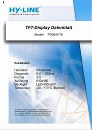
TFT-Display Datenblatt - Hy-Line
TFT-Display Datenblatt - Hy-Line
TFT-Display Datenblatt - Hy-Line

You also want an ePaper? Increase the reach of your titles
YUMPU automatically turns print PDFs into web optimized ePapers that Google loves.
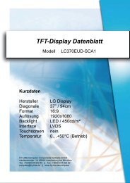
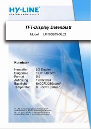
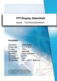
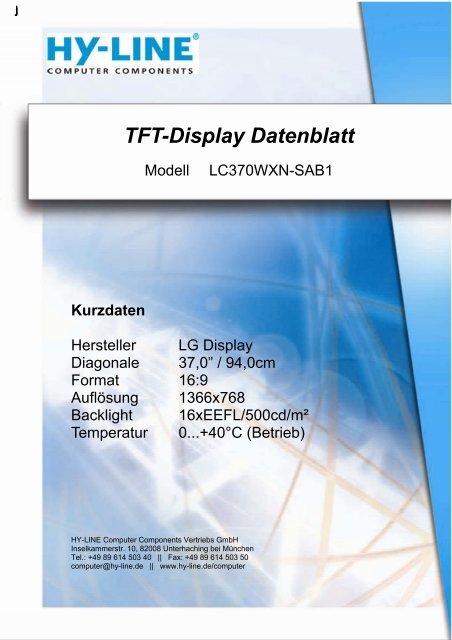
Kurzdaten<br />
<strong>TFT</strong>-<strong>Display</strong> <strong>Datenblatt</strong><br />
Modell LC370WXN-SAB1<br />
Hersteller LG <strong>Display</strong><br />
Diagonale 37,0” / 94,0cm<br />
Format 16:9<br />
Auflösung 1366x768<br />
Backlight 16xEEFL/500cd/m²<br />
Temperatur 0...+40°C (Betrieb)<br />
HY-LINE Computer Components Vertriebs GmbH<br />
Inselkammerstr. 10, 82008 Unterhaching bei München<br />
Tel.: +49 89 614 503 40 || Fax: +49 89 614 503 50<br />
computer@hy-line.de || www.hy-line.de/computer
(<br />
)<br />
( ) ●<br />
Ver. 1.0<br />
Preliminary Specification<br />
Final Specification<br />
BUYER<br />
MODEL<br />
Title<br />
APPROVED BY<br />
/<br />
/<br />
/<br />
General<br />
Please return 1 copy for your confirmation with<br />
your signature and comments.<br />
Product Specification<br />
SPECIFICATION<br />
SIGNATURE<br />
DATE<br />
FOR<br />
APPROVAL<br />
37.0” WXGA <strong>TFT</strong> LCD<br />
SUPPLIER<br />
*MODEL<br />
SUFFIX<br />
LC370WXN<br />
SAB1(RoHs Verified)<br />
LC370WXN<br />
LG.Philips LCD Co., Ltd.<br />
*When you obtain standard approval,<br />
please use the above model name without suffix<br />
APPROVED BY<br />
J.H. Lee / Senior Manager<br />
REVIEWED BY<br />
J.Y.Lee / Manager<br />
PREPARED BY<br />
S.Y. Choi / Engineer<br />
SIGNATURE<br />
DATE<br />
TV Product Development Dept.<br />
LG. Philips LCD Co., Ltd<br />
HY-LINE Computer Components / www.hy-line.de/computer<br />
1 / 34
Number<br />
1<br />
2<br />
3<br />
4<br />
5<br />
6<br />
7<br />
8<br />
9<br />
3-1<br />
3-2<br />
3-3<br />
3-4<br />
3-5<br />
3-6<br />
7-1<br />
7-2<br />
8-1<br />
8-2<br />
9-1<br />
9-2<br />
9-3<br />
9-4<br />
9-5<br />
9-6<br />
Ver. 1.0<br />
COVER<br />
CONTENTS<br />
RECORD OF REVISIONS<br />
GENERAL DESCRIPTION<br />
ABSOLUTE MAXIMUM RATINGS<br />
ELECTRICAL SPECIFICATIONS<br />
ELECTRICAL CHARACTERISTICS<br />
INTERFACE CONNECTIONS<br />
SIGNAL TIMING SPECIFICATIONS<br />
SIGNAL TIMING WAVEFORMS<br />
COLOR INPUT DATA REFERENCE<br />
POWER SEQUENCE<br />
OPTICAL SPECIFICATIONS<br />
MECHANICAL CHARACTERISTICS<br />
RELIABILITY<br />
INTERNATIONAL STANDARDS<br />
SAFETY<br />
EMC<br />
PACKING<br />
DESIGNATION OF LOT MARK<br />
PACKING FORM<br />
PRECAUTIONS<br />
MOUNTING PRECAUTIONS<br />
OPERATING PRECAUTIONS<br />
Product Specification<br />
Contents<br />
ELECTROSTATIC DISCHARGE CONTROL<br />
PRECAUTIONS FOR STRONG LIGHT EXPOSURE<br />
STORAGE<br />
ITEM<br />
HANDLING PRECAUTIONS FOR PROTECTION FILM<br />
HY-LINE Computer Components / www.hy-line.de/computer<br />
LC370WXN<br />
Page<br />
1<br />
2<br />
3<br />
4<br />
5<br />
6<br />
6<br />
8<br />
10<br />
11<br />
12<br />
13<br />
15<br />
19<br />
22<br />
23<br />
23<br />
23<br />
24<br />
24<br />
24<br />
25<br />
25<br />
25<br />
26<br />
26<br />
26<br />
26<br />
2 / 34
Revision No.<br />
1.0<br />
Ver. 1.0<br />
Revision Date<br />
Nov. 09, 2007<br />
Page<br />
-<br />
Product Specification<br />
Record of Revisions<br />
Final Specification<br />
Description<br />
HY-LINE Computer Components / www.hy-line.de/computer<br />
LC370WXN<br />
3 / 34
1. General Description<br />
Ver. 1.0<br />
Product Specification<br />
LC370WXN<br />
LC370WXN is a Color Active Matrix Liquid Crystal <strong>Display</strong> with an integral External Electrode Fluorescent<br />
Lamp(EEFL) backlight system. The matrix employs a-Si Thin Film Transistor as the active element.<br />
It is a transmissive type display operating in the normally black mode. It has a 37.02 inch diagonally<br />
measured active display area with WXGA resolution (768 vertical by 1366 horizontal pixel array)<br />
Each pixel is divided into Red, Green and Blue sub-pixels or dots which are arranged in vertical stripes.<br />
Gray scale or the luminance of the sub-pixel color is determined with a 8-bit gray scale signal for each dot,<br />
thus presenting a palette of more than 16.7M(true) colors.<br />
It has been designed to apply the 8-bit 1 port LVDS interface.<br />
It is intended to support LCD TV, PCTV where high brightness, super wide viewing angle, high color gamut,<br />
high color depth and fast response time are important.<br />
+12.0V<br />
LVDS<br />
5pair<br />
Select #9<br />
DCR_Enable#10<br />
VBR_EXT<br />
VBR_OUT<br />
General Features<br />
Pixel Pitch<br />
Pixel Format<br />
Color Depth<br />
Luminance, White<br />
Viewing Angle (CR>10)<br />
Power Consumption<br />
Weight<br />
#28<br />
#27<br />
CN3<br />
CN1<br />
(30pin)<br />
+24.0V<br />
V BR-A, V BR-B<br />
On/off<br />
Active Screen Size<br />
Outline Dimension<br />
<strong>Display</strong> Operating Mode<br />
Surface Treatment<br />
LUT Data<br />
DCR LUT, ODC LUT<br />
LVDS Rx (Receiver)<br />
DCR Controller<br />
ODC Controller<br />
Timing Controller<br />
Power Circuit<br />
Sync.<br />
PWM RGB<br />
Block Source Driver Circuit<br />
37.02 inches(940.3mm) diagonal<br />
877.0mm(H) x 516.8mm(V) x 55.5mm(D) (Typ.)<br />
0.200mm x 0.600mm x RGB<br />
1366 horiz. by 768 vert. pixels RGB stripe arrangement<br />
8-bit, 16.7 M colors<br />
500 cd/m 2 (Center 1 point Typ.)<br />
Viewing angle free ( R/L 178(Typ.), U/D 178(Typ.))<br />
Total 123.9 Watt (Typ.) (Logic= 3.9 W, B/L= 120 W [VBR-A=1.65V] )<br />
9000g (Typ.)<br />
LUT Data<br />
CN2, Inverter (14Pin, High)<br />
Gate Driver Circuit<br />
G1<br />
G768<br />
Transmissive mode, normally black<br />
<strong>TFT</strong> - LCD Panel<br />
(1366 × RGB × 768 pixels)<br />
S1 S1366<br />
Back light Assembly (16EEFL)<br />
Hard coating(3H), Anti-glare treatment of the front polarizer (Haze 13%)<br />
HY-LINE Computer Components / www.hy-line.de/computer<br />
4 / 34
2. Absolute Maximum Ratings<br />
Ver. 1.0<br />
Product Specification<br />
LC370WXN<br />
The followings are maximum values which, if exceeded, may cause faulty operation or damage to the unit.<br />
Table 1. ABSOLUTE MAXIMUM RATINGS<br />
Power Input<br />
Voltage<br />
Value<br />
Parameter Symbol<br />
Unit<br />
Remark<br />
Min<br />
Max<br />
LCM<br />
ON/OFF Control Voltage<br />
Brightness Control Voltage<br />
Operating Temperature<br />
Storage Temperature<br />
Backlight inverter<br />
Operating Ambient Humidity<br />
Storage Humidity<br />
VBL<br />
VBR<br />
TOP<br />
+22.5<br />
Note : 1. Temperature and relative humidity range are shown in the figure below.<br />
Wet bulb temperature should be 39 °C Max. and no condensation of water.<br />
2. Gravity mura can be guaranteed under<br />
℃<br />
40℃condition.<br />
-20<br />
Wet Bulb<br />
Temperature [°C]<br />
0<br />
0<br />
10<br />
20<br />
VLCD<br />
VON/OFF<br />
TST<br />
HOP<br />
HST<br />
30<br />
40<br />
+8.0<br />
-0.3<br />
0<br />
0<br />
-20<br />
10<br />
10<br />
90%<br />
+14.0<br />
+27.0<br />
+5.5<br />
+5.0<br />
+50<br />
+60<br />
90<br />
90<br />
10 20 30 40 50 60 70 80<br />
Dry Bulb Temperature [°C]<br />
50<br />
60<br />
VDC<br />
VDC<br />
VDC<br />
VDC<br />
%RH<br />
%RH<br />
Storage<br />
Operation<br />
HY-LINE Computer Components / www.hy-line.de/computer<br />
60%<br />
40%<br />
10%<br />
Humidity [(%)RH]<br />
at 25 ± 2 °C<br />
Note 1,2<br />
5 / 34
3. Electrical Specifications<br />
3-1. Electrical Characteristics<br />
Ver. 1.0<br />
Product Specification<br />
LC370WXN<br />
It requires two power inputs. One is employed to power the LCD electronics and to drive the <strong>TFT</strong> array and<br />
liquid crystal. The other input power for the EEFL/Backlight is to power inverter.<br />
Table 2. ELECTRICAL CHARACTERISTICS<br />
MODULE :<br />
Power Input Voltage<br />
Permissible Input Ripple Voltage<br />
Option High threshold<br />
VIH 2.3<br />
- 3.3 VDC<br />
Input Voltage Low threshold<br />
VIL<br />
0<br />
- 0.7 VDC<br />
Power Input Current<br />
Power Consumption<br />
Rush current<br />
Parameter Symbol<br />
VLCD<br />
VRP<br />
ILCD<br />
PLCD<br />
IRUSH<br />
Min<br />
11.4<br />
Note :<br />
1. The specified current and power consumption are under the V LCD =12.0V, 25 ± 2°C, f V =60Hz condition<br />
whereas mosaic pattern(8 x 6) is displayed and f V is the frame frequency.<br />
2. The current is specified at the maximum current pattern.<br />
3. The duration of rush current is about 2ms and rising time of power Input is 1ms(min.).<br />
White : 255Gray<br />
Black : 0Gray<br />
-<br />
-<br />
-<br />
-<br />
-<br />
Mosaic Pattern(8 x 6)<br />
Value<br />
12.0<br />
-<br />
326<br />
420<br />
3.9<br />
-<br />
Max<br />
12.6<br />
200<br />
424<br />
559<br />
HY-LINE Computer Components / www.hy-line.de/computer<br />
Typ<br />
5.1<br />
3.5<br />
Unit<br />
VDC<br />
mVP-P<br />
mA<br />
mA<br />
Watt<br />
A<br />
Note<br />
1<br />
2<br />
1<br />
3<br />
6 / 34
Ver. 1.0<br />
Product Specification<br />
Table 3. ELECTRICAL CHARACTERISTICS (Continue)<br />
Inverter :<br />
Power Supply Input Voltage<br />
Power Supply Input Voltage Ripple<br />
Power Supply<br />
Input Current<br />
Power Consumption<br />
Life Time<br />
LC370WXN<br />
Notes :<br />
1. Electrical characteristics are determined after the unit has been ‘ON’ and stable for approximately 120<br />
minutes at 25± 2°C. The specified current and power consumption are under the typical supply Input voltage<br />
24Vand VBR (VBR-A : 1.65V & VBR-B :3.3V), it is total power consumption.<br />
The ripple voltage of the power supply input voltage is under 0.5 Vp-p. LPL recommend Input Voltage is<br />
24.0V ± 5%.<br />
2. Electrical characteristics are determined within 30 minutes at 25± 2°C.<br />
The specified currents are under the typical supply Input voltage 24V.<br />
3. Brightness Control.<br />
This VBR-B Voltage control brightness.<br />
VBR-B Voltage<br />
After Aging<br />
Before Aging<br />
Power Supply Input Current (In-Rush)<br />
Input Voltage for<br />
Control System<br />
Signals<br />
Lamp:<br />
Parameter Symbol<br />
Brightness Adjust<br />
On/Off<br />
Brightness Adjust<br />
Function<br />
VBL<br />
IBL_A<br />
IBL_B<br />
Irush<br />
PBL<br />
VBR-A<br />
VBR-B<br />
50,000<br />
VBR-B Voltage<br />
Function<br />
0V<br />
Minimum Duty (20%)<br />
3.3V<br />
Maximum Duty (100%)<br />
.<br />
4. The brightness of the lamp after lighted for 5minutes is defined as 100%.<br />
TS is the time required for the brightness of the center of the lamp to be not less than 95% at typical current.<br />
The screen of LCD module may be partially dark by the time the brightness of lamp is stable after turn on.<br />
5. Specified Values are for a single lamp which is aligned horizontally.<br />
The life time is determined as the time which luminance of the lamp is 50% compared to that of initial value<br />
at the typical lamp current (VBR-A : 1.65V & VBR-B :3.3V), on condition of continuous operating at 25 ± 2°C<br />
6. The duration of rush current is about 10ms.<br />
Min<br />
22.8<br />
-<br />
-<br />
-<br />
-<br />
-<br />
-<br />
-<br />
0.0<br />
0<br />
Values<br />
Typ<br />
24.0<br />
-<br />
5.0<br />
5.5<br />
5.5<br />
6.0<br />
-<br />
120<br />
1.65<br />
-<br />
Max<br />
25.2<br />
0.5<br />
5.5<br />
6.0<br />
6.0<br />
6.5<br />
8<br />
132<br />
3.3<br />
3.3<br />
Unit<br />
Vdc<br />
Vp-p<br />
A<br />
A<br />
A<br />
A<br />
A<br />
W<br />
Vdc<br />
On V on 2.5 - 5.0 Vdc<br />
Off V off -0.3 0.0 0.8 Vdc<br />
HY-LINE Computer Components / www.hy-line.de/computer<br />
V<br />
Hrs<br />
Notes<br />
1<br />
1<br />
VBR-A = 1.65V …<br />
1<br />
VBR-A = 3.3V … 1<br />
VBR-A = 1.65V …<br />
2<br />
V BR-A = 3.3V … 2<br />
VBL = 22.8V<br />
VBR-B = 3.3V<br />
VBR-A = 1.65V<br />
VBR-A = 1.65V …<br />
1<br />
3<br />
4<br />
7 / 34
3-2. Interface Connections<br />
Ver. 1.0<br />
Product Specification<br />
Table 4. MODULE CONNECTOR(CN1) PIN CONFIGURATION<br />
Pin No.<br />
Symbol<br />
Description<br />
LC370WXN<br />
This LCD employs two kinds of interface connection, a 30-pin connector is used for the module electronics,<br />
14 Connectors are used for the integral backlight system.<br />
3-2-1. LCD Module<br />
- LCD Connector(CN1) : FI-X30SSL-HF (Manufactured by JAE) or Equivalent<br />
- Mating Connector : FI-X30C2L (Manufactured by JAE) or Equivalent<br />
1<br />
2<br />
3<br />
4<br />
5<br />
6<br />
7<br />
8<br />
9<br />
10<br />
11<br />
12<br />
13<br />
14<br />
15<br />
16<br />
17<br />
18<br />
19<br />
20<br />
21<br />
22<br />
23<br />
24<br />
25<br />
26<br />
27<br />
28<br />
29<br />
30<br />
VLCD Power Supply +12.0V<br />
VLCD<br />
VLCD<br />
VLCD<br />
GND<br />
GND<br />
GND<br />
GND<br />
Select<br />
DCR Enable<br />
GND<br />
RA-<br />
RA+<br />
GND<br />
RB-<br />
RB+<br />
GND<br />
RC-<br />
RC+<br />
GND<br />
RCLK-<br />
RCLK+<br />
GND<br />
RD-<br />
RD+<br />
GND<br />
VBR_OUT<br />
VBR_EXT<br />
Reserved<br />
GND<br />
Power Supply +12.0V<br />
Power Supply +12.0V<br />
Power Supply +12.0V<br />
Ground<br />
Ground<br />
Ground<br />
Ground<br />
Select LVDS Data format<br />
Dynamic CR Enable ( ‘L’ = Disable , ‘H’ = Enable )<br />
Ground<br />
LVDS Receiver Signal(-)<br />
LVDS Receiver Signal(+)<br />
Ground<br />
LVDS Receiver Signal(-)<br />
LVDS Receiver Signal(+)<br />
Ground<br />
LVDS Receiver Signal(-)<br />
LVDS Receiver Signal(+)<br />
Ground<br />
LVDS Receiver Clock Signal(-)<br />
LVDS Receiver Clock Signal(+)<br />
Ground<br />
LVDS Receiver Signal(-)<br />
LVDS Receiver Signal(+)<br />
Ground<br />
VBR output form LCD module<br />
External VBR input from System to LCD module<br />
Low or NC : Normal Operating<br />
High : Interlace Free Mode<br />
Ground<br />
Note: 1. If the pin no. 9 is Ground, Interface format is “LG”, and if the pin no. 9 is Vcc(3.3V), Interface format<br />
is “DISM”. See page 27 and 28.<br />
2. When this pin is no connection or Ground, DCR is Disabled.<br />
3. The pin no. 30 is necessary for LCD test.<br />
When LVDS signals are abnormal operation more than 3-Vsync times and power 12V is supplied,<br />
‘Open’ or ‘Vcc’ : LCD operate itself some test patterns.(AGP – Auto Generation Pattern)<br />
‘Ground’ : LCD operate itself a black pattern. (NSB – No Signal Black)<br />
LPL recommend ‘Ground’ for NSB.<br />
4. All GND (ground) pins should be connected together, which should be also connected to the LCD<br />
module’s metal frame.<br />
5. All VLCD (power input) pins should be connected together.<br />
6. Input Levels of LVDS signals are based on the IEA 664 Standard.<br />
HY-LINE Computer Components / www.hy-line.de/computer<br />
Note<br />
1<br />
2<br />
3<br />
8 / 34
3-2-2. Backlight Inverter<br />
Ver. 1.0<br />
Product Specification<br />
Inverter Connector : S14B-PH-SMC<br />
(manufactured by YeonHo) or Equivalent<br />
- Mating Connector : PHR-14 or Equivalent<br />
Table 5. INVERTER CONNECTOR PIN CONFIGULATION<br />
Pin No<br />
1<br />
2<br />
3<br />
4<br />
5<br />
6<br />
7<br />
8 GND Backlight Ground<br />
GND<br />
1<br />
9<br />
10<br />
11<br />
12<br />
13<br />
14<br />
Symbol<br />
VBL<br />
VBL<br />
VBL<br />
VBL<br />
VBL<br />
GND<br />
GND<br />
GND<br />
GND<br />
VBR-A<br />
VON/OFF<br />
VBR-B<br />
Status<br />
Backlight Ground<br />
Analog dimming voltage<br />
DC 0.0V ~ 3.3V (Typ : 1.65V)<br />
0.0V ~ 5.0V<br />
Description<br />
Power Supply +24.0V<br />
Power Supply +24.0V<br />
Power Supply +24.0V<br />
Power Supply +24.0V<br />
Power Supply +24.0V<br />
Backlight Ground<br />
Backlight Ground<br />
Backlight Ground<br />
Burst dimming voltage<br />
DC 0.0V ~ 3.3V<br />
Normal : Upper 3.0V<br />
Abnormal : Under 0.7V<br />
Inv.<br />
VBL<br />
VBL<br />
VBL<br />
VBL<br />
VBL<br />
GND<br />
GND<br />
GND<br />
GND<br />
VBR-A<br />
On/Off<br />
VBR-B<br />
Status<br />
Note<br />
2, 3<br />
3<br />
4<br />
LC370WXN<br />
Notes : 1. GND should be connected to the LCD module’s metal frame.<br />
2. If Pin #11 is open, VBR-A = 1.65V. When apply over 1.65V( ~ 3.3V) continuously,<br />
its luminance is increasing however lamp’s life time is decreasing.<br />
It could be usable for boost up luminance when using DCR (=Dynamic contrast ratio) function only.<br />
3. Minimum Brightness : VBR-B =0V Maximum Brightness : VBR-B = 3.3V<br />
4. Even though Pin #14 is open, there is no effect on inverter operating, The output terminal of inverter.<br />
5. Each impedance of pin #11,12 and 13 is 170[KΩ], 40[KΩ] , 60KΩ]<br />
◆Rear view of LCM<br />
14<br />
1<br />
…<br />
PCB<br />
…<br />
HY-LINE Computer Components / www.hy-line.de/computer<br />
9 / 34
3-3. Signal Timing Specifications<br />
Table 6. TIMING TABLE for NTSC<br />
Ver. 1.0<br />
Product Specification<br />
LC370WXN<br />
Table 6 and Table 7 show the signal timing required at the input of the LVDS transmitter. All of the interface<br />
signal timings should be satisfied with the following specification for normal operation.<br />
Vertical<br />
Horizontal<br />
Item<br />
DCLK Period<br />
DCLK Frequency<br />
Frequency<br />
Valid<br />
Blank<br />
Total<br />
Frequency<br />
Valid<br />
Blank<br />
Total<br />
Table 7. TIMING TABLE for PAL<br />
Vertical<br />
Horizontal<br />
Item<br />
DCLK Period<br />
DCLK Frequency<br />
Frequency<br />
Valid<br />
Blank<br />
Total<br />
Frequency<br />
Valid<br />
Blank<br />
Total<br />
Symbol<br />
t CLK<br />
f CLK<br />
f V<br />
t VV<br />
t VT - t VV<br />
t VT<br />
f H<br />
t HV<br />
t HT - t HV<br />
t HT<br />
Symbol<br />
t CLK<br />
f CLK<br />
f V<br />
t VV<br />
t VT - t VV<br />
t VT<br />
f H<br />
t HV<br />
t HT - t HV<br />
t HT<br />
Min. Typ. Max. Unit Notes<br />
12.5<br />
63.0<br />
57<br />
-<br />
8<br />
776<br />
45<br />
-<br />
90<br />
1456<br />
12.5<br />
63.0<br />
47<br />
-<br />
8<br />
776<br />
45<br />
-<br />
13.8<br />
72.4<br />
60<br />
768<br />
22<br />
790<br />
47.4<br />
1366<br />
162<br />
1528<br />
13.8<br />
72.4<br />
50<br />
768<br />
180<br />
948<br />
47.4<br />
1366<br />
15.8<br />
80.0<br />
63<br />
-<br />
295<br />
1063<br />
50<br />
-<br />
410<br />
1776<br />
15.8<br />
80.0<br />
53<br />
-<br />
295<br />
1063<br />
50<br />
-<br />
410<br />
1776<br />
nsec<br />
MHz<br />
Hz<br />
<strong>Line</strong><br />
<strong>Line</strong><br />
<strong>Line</strong><br />
KHz<br />
t CLK<br />
t CLK<br />
t CLK<br />
Min. Typ. Max. Unit Notes<br />
Note :<br />
1. The performance of the electro-optical characteristics may be influenced by variance of the vertical<br />
refresh rate.<br />
2. Above Timing Tables are only valid for DE Mode.<br />
90<br />
1456<br />
162<br />
1528<br />
nsec<br />
MHz<br />
Hz<br />
<strong>Line</strong><br />
<strong>Line</strong><br />
<strong>Line</strong><br />
KHz<br />
t CLK<br />
t CLK<br />
t CLK<br />
HY-LINE Computer Components / www.hy-line.de/computer<br />
10 / 34
3-4. Signal Timing Waveforms<br />
DCLK<br />
Data<br />
HSync<br />
Ver. 1.0<br />
tCLK<br />
DE(Data Enable)<br />
DE(Data Enable)<br />
VSync<br />
tWV<br />
DE(Data Enable)<br />
0.5 VDD<br />
Invalid data<br />
DE, Data<br />
* Reference : Sync. Relation<br />
tWH<br />
Product Specification<br />
Valid data<br />
tHP<br />
0.7VDD<br />
0.3VDD<br />
tHBP tHV tHFP<br />
tVP<br />
tVBP tVV tVFP<br />
HY-LINE Computer Components / www.hy-line.de/computer<br />
Invalid data<br />
LC370WXN<br />
* tHB = tHFP + tWH +tHBP<br />
* tVB = tVFP + tWV +tVBP<br />
11 / 34
3-5. Color Data Reference<br />
Ver. 1.0<br />
Product Specification<br />
LC370WXN<br />
The brightness of each primary color(red,green,blue) is based on the 8-bit gray scale data input for the color<br />
the higher the binary input, the brighter the color. The table below provides a reference for color versus data<br />
input.<br />
Table 8. COLOR DATA REFERENCE<br />
Basic<br />
Color<br />
RED<br />
GREEN<br />
BLUE<br />
Color<br />
Red (255)<br />
Green (255)<br />
Blue (255)<br />
Cyan<br />
Magenta<br />
Yellow<br />
White<br />
RED (000) Dark<br />
RED (001)<br />
...<br />
RED (254)<br />
RED (255)<br />
GREEN (000) Dark<br />
GREEN (001)<br />
...<br />
GREEN (254)<br />
GREEN (255)<br />
BLUE (000) Dark<br />
BLUE (001)<br />
...<br />
BLUE (254)<br />
BLUE (255)<br />
RED<br />
MSB LSB<br />
R7 R6 R5 R4 R3 R2 R1 R0<br />
Black 0 0 0 0 0 0 0 0 0 0 0 0 0 0 0 0 0 0 0 0 0 0 0 0<br />
1 1 1 1 1 1 1 1<br />
0 0 0 0 0 0 0 0<br />
0 0 0 0 0 0 0 0<br />
0 0 0 0 0 0 0 0<br />
1 1 1 1 1 1 1 1<br />
1 1 1 1 1 1 1 1<br />
1 1 1 1 1 1 1 1<br />
0 0 0 0 0 0 0 0<br />
0 0 0 0 0 0 0 1<br />
...<br />
1 1 1 1 1 1 1 0<br />
1 1 1 1 1 1 1 1<br />
0 0 0 0 0 0 0 0<br />
0 0 0 0 0 0 0 0<br />
...<br />
0 0 0 0 0 0 0 0<br />
0 0 0 0 0 0 0 0<br />
0 0 0 0 0 0 0 0<br />
0 0 0 0 0 0 0 0<br />
...<br />
0 0 0 0 0 0 0 0<br />
0 0 0 0 0 0 0 0<br />
Input Color Data<br />
GREEN<br />
MSB LSB<br />
G7 G6 G5 G4 G3 G2 G1 G0<br />
0 0 0 0 0 0 0 0<br />
1 1 1 1 1 1 1 1<br />
0 0 0 0 0 0 0 0<br />
1 1 1 1 1 1 1 1<br />
0 0 0 0 0 0 0 0<br />
1 1 1 1 1 1 1 1<br />
1 1 1 1 1 1 1 1<br />
0 0 0 0 0 0 0 0<br />
0 0 0 0 0 0 0 0<br />
...<br />
0 0 0 0 0 0 0 0<br />
0 0 0 0 0 0 0 0<br />
0 0 0 0 0 0 0 0<br />
0 0 0 0 0 0 0 1<br />
...<br />
1 1 1 1 1 1 1 0<br />
1 1 1 1 1 1 1 1<br />
0 0 0 0 0 0 0 0<br />
0 0 0 0 0 0 0 0<br />
...<br />
0 0 0 0 0 0 0 0<br />
0 0 0 0 0 0 0 0<br />
HY-LINE Computer Components / www.hy-line.de/computer<br />
BLUE<br />
MSB LSB<br />
B7 B6 B5 B4 B3 B2 B1 B0<br />
0 0 0 0 0 0 0 0<br />
0 0 0 0 0 0 0 0<br />
1 1 1 1 1 1 1 1<br />
1 1 1 1 1 1 1 1<br />
1 1 1 1 1 1 1 1<br />
0 0 0 0 0 0 0 0<br />
1 1 1 1 1 1 1 1<br />
0 0 0 0 0 0 0 0<br />
0 0 0 0 0 0 0 0<br />
...<br />
0 0 0 0 0 0 0 0<br />
0 0 0 0 0 0 0 0<br />
0 0 0 0 0 0 0 0<br />
0 0 0 0 0 0 0 0<br />
...<br />
0 0 0 0 0 0 0 0<br />
0 0 0 0 0 0 0 0<br />
0 0 0 0 0 0 0 0<br />
0 0 0 0 0 0 0 1<br />
...<br />
1 1 1 1 1 1 1 0<br />
1 1 1 1 1 1 1 1<br />
12 / 34
3-6. Power Sequence<br />
3-6-1. LCD Driving circuit<br />
Power Supply For LCD<br />
V LCD<br />
Interface Signal (Tx)<br />
Power for Lamp<br />
Table 9. POWER SEQUENCE<br />
Parameter<br />
Ver. 1.0<br />
T1<br />
T2<br />
T3<br />
T4<br />
T5<br />
T6<br />
T7<br />
T8<br />
0V<br />
Min<br />
0.5<br />
0.5<br />
200<br />
200<br />
0<br />
2.0<br />
0<br />
0<br />
10%<br />
90%<br />
Option Signal<br />
(LVDS_select, DCR_Enable, BIT_select)<br />
Product Specification<br />
Value<br />
Typ<br />
-<br />
-<br />
-<br />
-<br />
-<br />
-<br />
-<br />
-<br />
3 x (1/f V )<br />
LC370WXN<br />
Note : 1. Please avoid floating state of interface signal at invalid period.<br />
2. When the interface signal is invalid, be sure to pull down the power supply V LCD to 0V.<br />
3. The case when the T2/T5 exceed 3x(1/fv), it operates protection pattern (Black pattern) till valid<br />
signal inputted. There is no reliability problem. (ex. 60Hz : 3x(1/60Hz) = 50ms)<br />
4. The T3/T4 is recommended value, the case when failed to meet a minimum specification,<br />
abnormal display would be shown. There is no reliability problem.<br />
5. If the on time of signals(Interface signal and Option signals) precedes the on time of Power(V LCD ),<br />
check the LCD logic Power(Vcc) is under 0.8V, otherwise it will be happened abnormal display.<br />
6. T6 should be measured after the Module has been fully discharged between power off and on<br />
period.<br />
Max<br />
20<br />
-<br />
-<br />
-<br />
-<br />
T2<br />
-<br />
10%<br />
T1 T2 T5 T6<br />
T7<br />
Valid Data<br />
T3 T4<br />
Lamp ON<br />
T8<br />
90%<br />
HY-LINE Computer Components / www.hy-line.de/computer<br />
Unit<br />
ms<br />
ms<br />
ms<br />
ms<br />
ms<br />
s<br />
ms<br />
ms<br />
Notes<br />
3,5<br />
4<br />
4<br />
3,5<br />
2,6<br />
5<br />
5<br />
13 / 34
3-6-2. Sequence for Inverter<br />
Power Supply For Inverter<br />
Ver. 1.0<br />
VBL<br />
VON/OFF<br />
0V<br />
10%<br />
3-6-3. Deep condition for Inverter<br />
V BL (Typ.) x 0.8<br />
90%<br />
Table 10. Power Sequence for Inverter<br />
Parameter<br />
T1<br />
T2<br />
T3<br />
T4<br />
T5<br />
T6<br />
T7<br />
VBR-A &<br />
VBR-B<br />
Min<br />
20<br />
500<br />
200<br />
0<br />
10<br />
-<br />
2000<br />
Product Specification<br />
0.7V<br />
T1 T2 2000ms (Min) T5 T3 T2 1000ms (Min)<br />
T4<br />
-<br />
-<br />
T7<br />
Values<br />
Typ<br />
-<br />
-<br />
-<br />
-<br />
24V (typ.)<br />
Lamp ON<br />
T6<br />
T4<br />
V BL : 24V<br />
0 V<br />
V BL(Typ) x 0.8<br />
LC370WXN<br />
Notes : 1. T1 describes rising time of 0V to 24V and this parameter does not applied at restarting time.<br />
2. T4(max) is less than T2.<br />
3. In T7 section, V BR -B should be max level(3.3V) and V BR -A should be 1.65V.<br />
Max<br />
-<br />
-<br />
-<br />
-<br />
-<br />
10<br />
-<br />
Units<br />
HY-LINE Computer Components / www.hy-line.de/computer<br />
ms<br />
ms<br />
ms<br />
ms<br />
ms<br />
ms<br />
ms<br />
Remarks<br />
1<br />
2<br />
3<br />
14 / 34
4. Optical Specification<br />
Table 11. OPTICAL CHARACTERISTICS<br />
Ver. 1.0<br />
Optical Stage(x,y)<br />
LCD Module<br />
Product Specification<br />
50cm<br />
Pritchard 880 or<br />
equivalent<br />
FIG. 1 Optical Characteristic Measurement Equipment and Method<br />
LC370WXN<br />
Optical characteristics are determined after the unit has been ‘ON’ for 30min in a dark environment at 25± 2°C.<br />
The values specified are at an approximate distance 50cm from the LCD surface at a viewing angle of Φ and<br />
θ equal to 0 °.<br />
It is presented additional information concerning the measurement equipment and method in FIG. 1.<br />
Contrast Ratio<br />
CR<br />
DCR<br />
800<br />
-<br />
Ta= 25± 2°C, V LCD=12.0V, fV=60Hz, Dclk=72MHz,<br />
VBR_A =1.65V, VBR_B =3.3V, Except DCR Function<br />
1100<br />
-<br />
1<br />
Appendix 6<br />
Response Time G to G -<br />
5 10<br />
ms<br />
4<br />
Color Coordinates<br />
[CIE1931]<br />
Gray Scale<br />
Parameter<br />
Surface Luminance, white<br />
Luminance Variation<br />
Viewing Angle (CR>10)<br />
RED<br />
GREEN<br />
BLUE<br />
WHITE<br />
x axis, right(φ=0°)<br />
x axis, left (φ=180°)<br />
y axis, up (φ=90°)<br />
y axis, down (φ=270°)<br />
Symbol<br />
L WH<br />
δ WHITE<br />
Rx<br />
Ry<br />
Gx<br />
Gy<br />
Bx<br />
By<br />
Wx<br />
Wy<br />
θr<br />
θl<br />
θu<br />
θd<br />
5P<br />
Min<br />
400<br />
Typ<br />
-0.03<br />
89<br />
89<br />
89<br />
89<br />
Value<br />
500<br />
0.636<br />
0.335<br />
0.284<br />
0.610<br />
0.144<br />
0.063<br />
0.279<br />
0.292<br />
-<br />
-<br />
-<br />
-<br />
Max<br />
1.3<br />
Typ<br />
+0.03<br />
-<br />
-<br />
-<br />
-<br />
cd/m 2<br />
degree<br />
HY-LINE Computer Components / www.hy-line.de/computer<br />
Typ<br />
Unit<br />
Note<br />
2<br />
3<br />
5<br />
6<br />
15 / 34
Table 12. GRAY SCALE SPECIFICATION<br />
Ver. 1.0<br />
Product Specification<br />
Notes 1. Contrast Ratio(CR) is defined mathematically as :<br />
CR (Contrast Ratio) = Maximum CRn (n=1, 2, 3, 4, 5)<br />
DCR (Dynamic CR) = Maximum CRn (n=1, 2, 3, 4, 5)<br />
Surface Luminance at position n with all white pixels<br />
CRn =<br />
Surface Luminance at position n with all black pixels<br />
n = the Position number(1, 2, 3, 4, 5), For more information, see FIG 2.<br />
LC370WXN<br />
2. Surface luminance is luminance value at the center point across the LCD surface 50cm from the<br />
surface with all pixels displaying white.<br />
For more information, see FIG 2.<br />
3. The variation in surface luminance , δ WHITE is defined as :<br />
δ WHITE(5P) = Maximum(L on1 ,L on2 , L on3 , ...... , L on5 ) / Minimum(L on1 ,L on2 , L on3 , ..... , L on5 )<br />
Where L on1 to L on5 are the luminance with all pixels displaying white at 5 locations .<br />
For more information, see FIG 2.<br />
4. Response time is the time required for the display to transition from G(N) to G(M) (Rise Time, Tr R )<br />
and from G(M) to G(N) (Decay Time, Tr D ). For additional information see the FIG. 3. (N
Product Specification<br />
Measuring point for surface luminance & measuring point for luminance variation<br />
V<br />
Ver. 1.0<br />
B<br />
②<br />
④<br />
A<br />
①<br />
H<br />
③<br />
⑤<br />
FIG. 2 Measure Point for Luminance<br />
FIG. 3 Response Time<br />
LC370WXN<br />
A : H / 4 mm<br />
B : V / 4 mm<br />
H : 819.6 mm<br />
V : 460.8 mm<br />
@ H,V : Active Area<br />
Response time is defined as the following figure and shall be measured by switching the input signal for<br />
“Gray(N)” and “Gray(M)”.<br />
%<br />
100<br />
90<br />
Optical<br />
Response<br />
10<br />
0<br />
Gray(N)<br />
TrR TrD<br />
Gray(M)<br />
N,M = 0(Black)~255(White), N
Dimension of viewing angle range<br />
φ = 180 °, Left<br />
Ver. 1.0<br />
φ = 270 °, Down<br />
Product Specification<br />
Normal<br />
θ<br />
φ<br />
FIG. 4 Viewing angle<br />
E<br />
Y<br />
φ = 90 °, Up<br />
φ = 0 °, Right<br />
HY-LINE Computer Components / www.hy-line.de/computer<br />
LC370WXN<br />
18 / 34
5. Mechanical Characteristics<br />
Ver. 1.0<br />
Product Specification<br />
LC370WXN<br />
The following items provide general mechanical characteristics. In addition the figures in the next page are<br />
detailed mechanical drawing of the LCD module.<br />
Table 13. MECHANICAL CHARACTERISTICS<br />
Outline Dimension<br />
Bezel Area<br />
Active <strong>Display</strong> Area<br />
Weight<br />
Surface Treatment<br />
Horizontal<br />
Vertical<br />
Depth<br />
Horizontal<br />
Vertical<br />
Horizontal<br />
Vertical<br />
9000g(Typ.)/9300g(Max)<br />
877.0 mm<br />
516.8 mm<br />
55.5 mm<br />
828.6mm<br />
469.8mm<br />
819.6mm<br />
460.8mm<br />
Hard coating(3H)<br />
Anti-glare treatment of the front polarizer, Haze 13%<br />
Note : Please refer to a mechanic drawing in terms of tolerance at the next page.<br />
HY-LINE Computer Components / www.hy-line.de/computer<br />
19 / 34
Ver. 1.0<br />
Product Specification<br />
HY-LINE Computer Components / www.hy-line.de/computer<br />
LC370WXN<br />
20 / 34
Ver. 1.0<br />
Product Specification<br />
LC370WXN<br />
Notes : It should be recommended that any exterior materials do not go passing up the red area slanted.<br />
( For example, electrical cable, system board , etc ). Otherwise, it could cause that abnormal<br />
display happens.<br />
HY-LINE Computer Components / www.hy-line.de/computer<br />
21 / 34
6. Reliability<br />
Table 14. ENVIRONMENT TEST CONDITION<br />
No.<br />
1<br />
2<br />
3<br />
4<br />
5<br />
6<br />
7<br />
Ver. 1.0<br />
Vibration test<br />
(non-operating)<br />
Shock test<br />
(non-operating)<br />
Test Item<br />
High temperature storage test<br />
Low temperature storage test<br />
High temperature operation test<br />
Low temperature operation test<br />
Humidity condition Operation<br />
Product Specification<br />
Ta= 50°C 240h<br />
Ta= -20°C 240h<br />
Ta= 40°C 50%RH 240h<br />
Ta= 0°C 240h<br />
Wave form : random<br />
Vibration level : 1.0G RMS<br />
Bandwidth : 10-500Hz<br />
Duration : X,Y,Z, 10 min<br />
One time each direction<br />
Shock level : 100G<br />
Waveform : half sine wave, 2ms<br />
Direction :±X, ±Y, ±Z<br />
One time each direction<br />
Ta= 40 °C, 90%RH<br />
Condition<br />
Note : Before and after Reliability test, LCM should be operated with normal function.<br />
HY-LINE Computer Components / www.hy-line.de/computer<br />
LC370WXN<br />
22 / 34
7. International Standards<br />
7-1. Safety<br />
Ver. 1.0<br />
Product Specification<br />
a) UL 60065, 7 th Edition, dated June 30, 2003, Underwriters Laboratories, Inc.,<br />
Standard for Audio, Video and Similar Electronic Apparatus.<br />
b) CAN/CSA C22.2, No. 60065:03, Canadian Standards Association,<br />
Standard for Audio, Video and Similar Electronic Apparatus.<br />
c) IEC60065:2001, 7 th Edition CB-scheme and EN 60065:2002,<br />
Safety requirements for Audio, Video and Similar Electronic Apparatus..<br />
7-2. EMC<br />
LC370WXN<br />
a) ANSI C63.4 “Methods of Measurement of Radio-Noise Emissions from Low-Voltage Electrical and<br />
Electrical Equipment in the Range of 9kHZ to 40GHz. “American National Standards Institute(ANSI),<br />
1992<br />
b) CISPR13 "Limits and Methods of Measurement of Radio interference characteristics of Sound<br />
and Television broadcast receivers and associated equipment"<br />
CISPR22 "Limits and Methods of Measurement of Radio interference characteristics of Information<br />
Technology Equipment" International Special Committee on Radio Interference.<br />
c) EN55013 "Limits and Methods of Measurement of Radio interference characteristics of Sound and<br />
Television broadcast receivers and associated equipment"<br />
EN55022 "Limits and Methods of Measurement of Radio interference characteristics of Information<br />
Technology Equipment" European Committee for Electro Technical Standardization.(CENELEC),<br />
1988(Including A1:2000)<br />
HY-LINE Computer Components / www.hy-line.de/computer<br />
23 / 34
8. Packing<br />
8-1. Designation of Lot Mark<br />
a) Lot Mark<br />
Ver. 1.0<br />
Product Specification<br />
A B C D E F G H I J K L M<br />
A,B,C : SIZE(INCH) D : YEAR<br />
E : MONTH F ~ M : SERIAL NO.<br />
Note<br />
1. YEAR<br />
Year<br />
Mark<br />
2. MONTH<br />
Month<br />
Mark<br />
8-2. Packing Form<br />
2001<br />
a) LCM quantity in one box : 4 pcs<br />
b) Box Size : 968mm X 366mm X 595mm<br />
1<br />
Jan<br />
b) Location of Lot Mark<br />
1<br />
2002<br />
2<br />
Feb<br />
2<br />
2003<br />
3<br />
Mar<br />
3<br />
2004<br />
4<br />
Apr<br />
4<br />
2005<br />
5<br />
May<br />
5<br />
2006<br />
6<br />
Jun<br />
6<br />
2007<br />
7<br />
Jul<br />
7<br />
2008<br />
8<br />
Aug<br />
8<br />
2009<br />
9<br />
Sep<br />
9<br />
2010<br />
Serial No. is printed on the label. The label is attached to the backside of the LCD module.<br />
This is subject to change without prior notice.<br />
HY-LINE Computer Components / www.hy-line.de/computer<br />
0<br />
Oct<br />
A<br />
LC370WXN<br />
Nov<br />
B<br />
Dec<br />
C<br />
24 / 34
9. Precautions<br />
Product Specification<br />
Please pay attention to the followings when you use this <strong>TFT</strong> LCD module.<br />
Ver. 1.0<br />
LC370WXN<br />
9-1. Mounting Precautions<br />
(1) You must mount a module using specified mounting holes (Details refer to the drawings).<br />
(2) You should consider the mounting structure so that uneven force (ex. Twisted stress) is not applied to the<br />
module. And the case on which a module is mounted should have sufficient strength so that external<br />
force is not transmitted directly to the module.<br />
(3) Please attach the surface transparent protective plate to the surface in order to protect the polarizer.<br />
Transparent protective plate should have sufficient strength in order to the resist external force.<br />
(4) You should adopt radiation structure to satisfy the temperature specification.<br />
(5) Acetic acid type and chlorine type materials for the cover case are not desirable because the former<br />
generates corrosive gas of attacking the polarizer at high temperature and the latter causes circuit break<br />
by electro-chemical reaction.<br />
(6) Do not touch, push or rub the exposed polarizers with glass, tweezers or anything harder than HB<br />
pencil lead. And please do not rub with dust clothes with chemical treatment.<br />
Do not touch the surface of polarizer for bare hand or greasy cloth.(Some cosmetics are detrimental<br />
to the polarizer.)<br />
(7) When the surface becomes dusty, please wipe gently with absorbent cotton or other soft materials like<br />
chamois soaks with petroleum benzine. Normal-hexane is recommended for cleaning the adhesives<br />
used to attach front / rear polarizers. Do not use acetone, toluene and alcohol because they cause<br />
chemical damage to the polarizer.<br />
(8) Wipe off saliva or water drops as soon as possible. Their long time contact with polarizer causes<br />
deformations and color fading.<br />
(9) Do not open the case because inside circuits do not have sufficient strength.<br />
9-2. Operating Precautions<br />
(1) The spike noise causes the mis-operation of circuits. It should be lower than following voltage :<br />
V=± 200mV(Over and under shoot voltage)<br />
(2) Response time depends on the temperature.(In lower temperature, it becomes longer.)<br />
(3) Brightness depends on the temperature. (In lower temperature, it becomes lower.)<br />
And in lower temperature, response time(required time that brightness is stable after turned on)<br />
becomes longer<br />
(4) Be careful for condensation at sudden temperature change.Condensation makes damage to polarizer or<br />
electrical contacted parts. And after fading condensation, smear or spot will occur.<br />
(5) When fixed patterns are displayed for a long time, remnant image is likely to occur.<br />
(6) Module has high frequency circuits. Sufficient suppression to the electromagnetic interference shall be<br />
done by system manufacturers. Grounding and shielding methods may be important to minimized the<br />
interference.<br />
(7) Please do not give any mechanical and/or acoustical impact to LCM. Otherwise, LCM can’t be operated<br />
its full characteristics perfectly.<br />
(8) A screw which is fastened up the steels should be a machine screw.<br />
(if not, it can causes conductive particles and deal LCM a fatal blow)<br />
(9) Please do not set LCD on its edge.<br />
(10) It is recommended to avoid the signal cable and conductive material over the inverter transformer<br />
for it can cause the abnormal display and temperature rising.<br />
HY-LINE Computer Components / www.hy-line.de/computer<br />
25 / 34
Product Specification<br />
LC370WXN<br />
9-3. Electrostatic Discharge Control<br />
Since a module is composed of electronic circuits, it is not strong to electrostatic discharge. Make certain that<br />
treatment persons are connected to ground through wrist band etc. And don’t touch interface pin directly.<br />
9-4. Precautions for Strong Light Exposure<br />
Strong light exposure causes degradation of polarizer and color filter.<br />
9-5. Storage<br />
When storing modules as spares for a long time, the following precautions are necessary.<br />
(1) Store them in a dark place. Do not expose the module to sunlight or fluorescent light. Keep the temperature<br />
between 5°C and 35°C at normal humidity.<br />
(2) The polarizer surface should not come in contact with any other object.<br />
It is recommended that they be stored in the container in which they were shipped.<br />
9-6. Handling Precautions for Protection Film<br />
(1) The protection film is attached to the bezel with a small masking tape.<br />
When the protection film is peeled off, static electricity is generated between the film and polarizer.<br />
This should be peeled off slowly and carefully by people who are electrically grounded and with well ionblown<br />
equipment or in such a condition, etc.<br />
(2) When the module with protection film attached is stored for a long time, sometimes there remains a very<br />
small amount of glue still on the bezel after the protection film is peeled off.<br />
(3) You can remove the glue easily. When the glue remains on the bezel surface or its vestige is recognized,<br />
please wipe them off with absorbent cotton waste or other soft material like chamois soaked with normalhexane.<br />
Ver. 1.0<br />
HY-LINE Computer Components / www.hy-line.de/computer<br />
26 / 34
Appendix 1-1.<br />
Host System<br />
24 Bit<br />
Ver. 1.0<br />
RED0<br />
RED1<br />
RED2<br />
RED3<br />
RED4<br />
RED5<br />
RED6<br />
RED7<br />
GREEN0<br />
GREEN1<br />
GREEN2<br />
GREEN3<br />
GREEN4<br />
GREEN5<br />
GREEN6<br />
GREEN7<br />
BLUE0<br />
BLUE1<br />
BLUE2<br />
BLUE3<br />
BLUE4<br />
BLUE5<br />
BLUE6<br />
BLUE7<br />
Hsync<br />
Vsync<br />
Data Enable<br />
CLOCK<br />
Product Specification<br />
■ REQUIRED SIGNAL ASSIGNMENT FOR LVDS TRANSMITTER ( Pin9=“L” )<br />
51<br />
52<br />
54<br />
55<br />
56<br />
3<br />
50<br />
2<br />
4<br />
6<br />
7<br />
11<br />
12<br />
14<br />
8<br />
10<br />
15<br />
19<br />
20<br />
22<br />
23<br />
24<br />
16<br />
18<br />
27<br />
28<br />
30<br />
31<br />
DS90C385<br />
or Compatible<br />
TxOUT0-<br />
TxOUT0+<br />
TxOUT1-<br />
TxOUT1+<br />
TxOUT2-<br />
TxOUT2+<br />
TxCLKOUT-<br />
TxCLKOUT+<br />
TxOUT3-<br />
TxOUT3+<br />
LC370WXN<br />
Note: 1. The LCD Module uses a 100 Ohm[Ω] resistor between positive and negative lines of each receiver<br />
input.<br />
2. Refer to LVDS Transmitter Data Sheet for detail descriptions. (DS90C385 or Compatible)<br />
3. ‘7’ means MSB and ‘0’ means LSB at R,G,B pixel data.<br />
48<br />
47<br />
46<br />
45<br />
42<br />
41<br />
40<br />
39<br />
38<br />
37<br />
FI-X30SSL-HF<br />
12<br />
13<br />
15<br />
16<br />
18<br />
19<br />
21<br />
22<br />
24<br />
25<br />
9<br />
30<br />
100Ω<br />
100Ω<br />
100Ω<br />
100Ω<br />
1KΩ<br />
100Ω<br />
150Ω<br />
LCD Module<br />
HY-LINE Computer Components / www.hy-line.de/computer<br />
GND<br />
GND<br />
Timing<br />
Controller<br />
RxIN0-<br />
RxIN0+<br />
RxIN1-<br />
RxIN1+<br />
RxIN2-<br />
RxIN2+<br />
RxCLKIN-<br />
RxCLKIN+<br />
RxIN3-<br />
RxIN3+<br />
LG / DISM<br />
LCD Test<br />
27 / 34
Appendix 1-2.<br />
Host System<br />
24 Bit<br />
Ver. 1.0<br />
RED0<br />
RED1<br />
RED2<br />
RED3<br />
RED4<br />
RED5<br />
RED6<br />
RED7<br />
GREEN0<br />
GREEN1<br />
GREEN2<br />
GREEN3<br />
GREEN4<br />
GREEN5<br />
GREEN6<br />
GREEN7<br />
BLUE0<br />
BLUE1<br />
BLUE2<br />
BLUE3<br />
BLUE4<br />
BLUE5<br />
BLUE6<br />
BLUE7<br />
Hsync<br />
Vsync<br />
Data Enable<br />
CLOCK<br />
Product Specification<br />
■ REQUIRED SIGNAL ASSIGNMENT FOR LVDS TRANSMITTER ( Pin9=“H” )<br />
50<br />
2<br />
51<br />
52<br />
54<br />
55<br />
56<br />
3<br />
8<br />
10<br />
4<br />
6<br />
7<br />
11<br />
12<br />
14<br />
16<br />
18<br />
15<br />
19<br />
20<br />
22<br />
23<br />
24<br />
27<br />
28<br />
30<br />
31<br />
DS90C385<br />
or Compatible<br />
TxOUT0-<br />
TxOUT0+<br />
TxOUT1-<br />
TxOUT1+<br />
TxOUT2-<br />
TxOUT2+<br />
TxCLKOUT-<br />
TxCLKOUT+<br />
TxOUT3-<br />
TxOUT3+<br />
48<br />
47<br />
46<br />
45<br />
42<br />
41<br />
40<br />
39<br />
38<br />
37<br />
Vcc<br />
FI-X30SSL-HF<br />
GND<br />
12<br />
13<br />
15<br />
16<br />
18<br />
19<br />
21<br />
22<br />
24<br />
25<br />
9<br />
30<br />
100Ω<br />
100Ω<br />
100Ω<br />
100Ω<br />
1KΩ<br />
100Ω<br />
150Ω<br />
LCD Module<br />
RxIN0-<br />
RxIN0+<br />
RxIN1-<br />
RxIN1+<br />
RxIN2-<br />
RxIN2+<br />
RxCLKIN-<br />
RxCLKIN+<br />
RxIN3-<br />
RxIN3+<br />
LG / DISM<br />
LCD Test<br />
LC370WXN<br />
Timing<br />
Controller<br />
Note: 1. The LCD Module uses a 100 Ohm[Ω] resistor between positive and negative lines of each receiver<br />
input.<br />
2. Refer to LVDS Transmitter Data Sheet for detail descriptions. (DS90C385 or Compatible)<br />
3. ‘7’ means MSB and ‘0’ means LSB at R,G,B pixel data.<br />
HY-LINE Computer Components / www.hy-line.de/computer<br />
28 / 34
# APPENDIX 3<br />
Appendix 2-1<br />
■ LCM DCR Only<br />
DCR_Enable<br />
V BR -B<br />
V BR -A<br />
DCR Level<br />
Ver. 1.0<br />
LCM<br />
LCM<br />
Master<br />
Master<br />
Inverter<br />
Inverter<br />
14<br />
14<br />
1<br />
FFC FFC FFC Cable<br />
Cable<br />
Cable<br />
On(3.3V)<br />
0V ~ 3.3V<br />
1.65V or NC<br />
2200 : 1<br />
System System<br />
System<br />
Board<br />
13 13<br />
13<br />
11<br />
11<br />
11<br />
Product Specification<br />
LCM LCM Control Control Board<br />
Board<br />
3.3V<br />
NTSC NTSC / / / / / / / PAL<br />
PAL<br />
Sync_PWM<br />
Sync_PWM<br />
1<br />
12V<br />
12V<br />
Off (0V)<br />
30 30<br />
1<br />
VBR VBR<br />
VBR - B<br />
3.3V<br />
3.3V<br />
VBR VBR<br />
VBR - A<br />
NC NC NC / / 1.65V<br />
1.65V<br />
1.65V or NC<br />
1100 : 1<br />
10<br />
10<br />
Analog Switch<br />
LCM VBR-B<br />
DCR_Enable DCR_Enable “H”<br />
LCM VBR-B<br />
Gray Level<br />
L111<br />
L127<br />
L143<br />
L159<br />
L175<br />
L191<br />
L207<br />
L223<br />
L239<br />
L255<br />
3.3V 3.3V<br />
3.3V<br />
HY-LINE Computer Components / www.hy-line.de/computer<br />
L0<br />
L15<br />
L31<br />
L47<br />
L63<br />
L79<br />
L95<br />
27<br />
28<br />
28<br />
30<br />
30<br />
0.045<br />
0.33<br />
1.10<br />
2.81<br />
5.40<br />
8.5<br />
12.4<br />
16.7<br />
21.3<br />
27.4<br />
34.6<br />
43.0<br />
52.4<br />
63.0<br />
74.5<br />
86.8<br />
100<br />
LC370WXN<br />
Luminance [%] DCR On<br />
VBR-A = 1.65V<br />
29 / 34
# APPENDIX 3<br />
Appendix 2-2<br />
Ver. 1.0<br />
LCM<br />
LCM<br />
Master<br />
Master<br />
Inverter Inverter<br />
Inverter<br />
14<br />
14<br />
1<br />
FFC FFC FFC Cable Cable Cable Cable<br />
Cable<br />
Cable<br />
LCM LCM Control Control Board<br />
Board<br />
System<br />
System<br />
Board<br />
13<br />
13<br />
11<br />
11<br />
11<br />
NTSC NTSC / / / / / / / PAL<br />
PAL<br />
Sync_PWM<br />
Sync_PWM<br />
1<br />
12V<br />
12V<br />
Product Specification<br />
■ System DCR (Dynamic Contrast Ratio)- Max 5500:1<br />
V BR -B<br />
V BR -A<br />
DCR Level<br />
0V ~ 3.3V<br />
0V ~ 3.3V<br />
5500 : 1<br />
30 30<br />
1<br />
VBR VBR<br />
VBR - B<br />
0 ~ 3.3V<br />
VBR VBR<br />
VBR - A<br />
0 ~ 3.3V<br />
3.3V<br />
1.65V<br />
1100 : 1<br />
10<br />
10<br />
Analog Switch<br />
LCM VBR-B<br />
DCR_Enable DCR_Enable “L”<br />
3.3V<br />
3.3V<br />
Note : 1. To make DCR Max 5500:1, V BR -A and V BR -B must be given by system.<br />
2. DCR Max 5500:1 is defined mathematically as :<br />
DCR = Maximum DCRn (n=1, 2, 3, 4, 5)<br />
27<br />
28<br />
28<br />
30<br />
30<br />
LC370WXN<br />
Surface Luminance at position n with all white pixels (VBR-B=3.3V, VBR-A=3.3V)<br />
DCRn = Surface Luminance at position n with all black pixels (VBR-B=0V, VBR-A=0V)<br />
n = the Position number(1, 2, 3, 4, 5). For more information, see FIG 2.<br />
HY-LINE Computer Components / www.hy-line.de/computer<br />
30 / 34
Appendix 3<br />
■LC370WXN-SAB1 Packing Ass’y<br />
Ver. 1.0<br />
NO.<br />
1<br />
2<br />
3<br />
4<br />
5<br />
6<br />
7<br />
8<br />
Product Specification<br />
DESCRIPTION<br />
LCD MODULE<br />
BAG<br />
TAPE<br />
PACKING, BOTTOM<br />
PACKING, TOP R_L<br />
BOX<br />
TAPE<br />
LABEL<br />
HY-LINE Computer Components / www.hy-line.de/computer<br />
MATERIAL<br />
AL<br />
EPS<br />
EPS<br />
PAPER_DW3<br />
OPP 70MMX300M<br />
YUPO PAPER 100X100<br />
LC370WXN<br />
MASKING 20MM X 50M<br />
31 / 34
# APPENDIX 2<br />
Appendix 4<br />
■ LC370WXN-SAB1 Pallet Ass’y<br />
Ver. 1.0<br />
NO.<br />
1<br />
2<br />
3<br />
4<br />
5<br />
6<br />
7<br />
Product Specification<br />
DESCRIPTION<br />
PACKING ASS’Y<br />
PALLET<br />
ANGLE, PACKING<br />
LABEL<br />
TAPE<br />
BAND<br />
BAND, CLIP<br />
MATERIAL<br />
Paper_1140X990X117.5<br />
SWR4<br />
YUPO PAPER<br />
OPP<br />
PP<br />
CLIP 18MM<br />
HY-LINE Computer Components / www.hy-line.de/computer<br />
LC370WXN<br />
32 / 34
# APPENDIX 3<br />
Appendix 5<br />
■ LCM Label<br />
a) GUMI<br />
Ver. 1.0<br />
Model<br />
UL, TUV Mark<br />
LPL Logo<br />
US PATENT No.<br />
b) CHINA<br />
Model<br />
UL, TUV Mark<br />
LPL Logo<br />
US PATENT No.<br />
LC370WXN<br />
(SA)(B1)<br />
RoHS Verified<br />
Product Specification<br />
1 2 3 4 5 6 7 8 9 10 11 12<br />
********** ***<br />
■ Serial No. (See CAS 24page for more information)<br />
Inch<br />
Year Month<br />
LC370WXN<br />
(SA)(B1)<br />
RoHS Verified<br />
Serial No.<br />
M Ass’y Factory code<br />
13<br />
MADE IN KOREA<br />
********** ***<br />
MADE IN KOREA<br />
Made in CHINA<br />
HY-LINE Computer Components / www.hy-line.de/computer<br />
LC370WXN<br />
Origin<br />
Origin<br />
Serial No.<br />
Serial No.<br />
33 / 34
# APPENDIX 4<br />
Appendix 6<br />
Ver. 1.0<br />
Product Specification<br />
■ Box Label ■ Pallet Label<br />
4 PCS<br />
LC370WXN<br />
SAB1<br />
RoHS Verified<br />
LC370WXN<br />
12 PCS<br />
SAB1<br />
HY-LINE Computer Components / www.hy-line.de/computer<br />
LC370WXN<br />
RoHS Verified<br />
34 / 34