TN1246 - Lattice Semiconductor Corporation
TN1246 - Lattice Semiconductor Corporation
TN1246 - Lattice Semiconductor Corporation

Create successful ePaper yourself
Turn your PDF publications into a flip-book with our unique Google optimized e-Paper software.
October 2012 Technical Note <strong>TN1246</strong><br />
Introduction<br />
This reference guide supplements TN1205, Using User Flash Memory and Hardened Control Functions in<br />
MachXO2 Devices Usage Guide which explains the software usage. In this document you will find:<br />
WISHBONE Protocol<br />
EFB Register Map<br />
Command Sequences<br />
Examples<br />
As an overview, the MachXO2 FPGA family combines a high-performance, low power, FPGA fabric with built-in,<br />
hardened control functions and on-chip User Flash Memory (UFM). The hardened control functions ease design<br />
implementation and save general purpose resources such as LUTs, registers, clocks and routing. The hardened<br />
control functions are physically located in the Embedded Function Block (EFB). All MachXO2 devices include an<br />
EFB module. The EFB block includes the following control functions:<br />
Two I2C Cores<br />
One SPI Core<br />
One 16-bit Timer/Counter<br />
Interface to Flash Memory which includes:<br />
– User Flash Memory for MachXO2-640 and higher densities<br />
– Configuration Logic<br />
Interface to Dynamic PLL configuration settings<br />
Interface to On-chip Power Controller through I2C and SPI<br />
Using User Flash Memory and<br />
Hardened Control Functions in<br />
MachXO2 Devices Reference Guide<br />
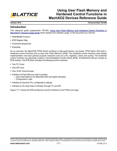
Figure 17-1 shows the EFB architecture and the interface to the FPGA core logic.<br />
© 2012 <strong>Lattice</strong> <strong>Semiconductor</strong> Corp. All <strong>Lattice</strong> trademarks, registered trademarks, patents, and disclaimers are as listed at www.latticesemi.com/legal. All other brand<br />
or product names are trademarks or registered trademarks of their respective holders. The specifications and information herein are subject to change without notice.<br />
www.latticesemi.com 17-1 tn1246_01.2
Figure 17-1. Embedded Function Block (EFB)<br />
User Logic<br />
User Logic<br />
EFB Register Map<br />
WISHBONE Interface<br />
Using User Flash Memory and Hardened<br />
Control Functions in MachXO2 Devices Reference Guide<br />
The EFB module has a Register Map to allow the service of the hardened functions through the WISHBONE bus<br />
interface read/write operations. Each hardened function has dedicated 8-bit Data and Control registers, with the<br />
exception of the Flash Memory (UFM/Configuration), which are accessed through the same set of registers.<br />
Table 17-1 documents the register map of the EFB module. The PLL registers are located in the MachXO2 PLL<br />
modules, but they are accessed through EFB WISHBONE read/write cycles.<br />
Table 17-1. EFB Register Map<br />
EFB Register Map<br />
Configuration<br />
(including<br />
USERCODE)<br />
Flash Memory<br />
UFM<br />
Flash Command Interface<br />
EFB<br />
PLL0/<br />
PLL1<br />
Address (Hex) Hardened Function<br />
0x00-0x1F PLL0 Dynamic Access1<br />
0x20-0x3F PLL1 Dynamic Access1<br />
0x40-0x49 I2C Primary<br />
0x4A-0x53 I2C Secondary<br />
0x54-0x5D SPI<br />
0x5E-0x6F Timer/Counter<br />
0x70-0x75 Flash Memory (UFM/Configuration)<br />
0x76-0x77 EFB Interrupt Source<br />
1. There can be up to two PLLs in a MachXO2 device. PLL0 has<br />
an address range from 0x00 to 0x1F. PLL1 (if present) has an<br />
address range from 0x20 to 0x3F. Reference TN1199,<br />
MachXO2 sysCLOCK PLL Design and Usage Guide, for details<br />
on PLL configuration registers and recommended usage.<br />
Address spaces that are not defined in Table 17-1 are invalid and will result in non-deterministic results. It is the<br />
responsibility of the designer to ensure valid addresses are presented to the EFB WISHBONE slave interface.<br />
17-2<br />
Feature Row<br />
(including<br />
TraceID)<br />
Power<br />
Controller<br />
Configuration<br />
Slave<br />
User<br />
Master/Slave<br />
User<br />
Master/Slave<br />
Configuration<br />
Master/Slave<br />
User<br />
Master/Slave<br />
Timer/<br />
Counter<br />
OR<br />
JTAG<br />
Primary<br />
I 2 C Port<br />
Secondary<br />
I 2 C Port<br />
SPI Port
WISBONE Bus Interface<br />
Using User Flash Memory and Hardened<br />
Control Functions in MachXO2 Devices Reference Guide<br />
The WISHBONE Bus in the MachXO2 is compliant with the WISHBONE standard from OpenCores. It provides<br />
connectivity between FPGA user logic and the EFB functional blocks. The user can implement a WISHBONE Master<br />
interface to interact with the EFB WISHBONE slave interface or a <strong>Lattice</strong>Mico8 soft processor core can be<br />
used to interact with the EFB WISHBONE.<br />
The block diagram in Figure 17-2 shows the supported WISHBONE bus signals between the FPGA core and the<br />
EFB. Table 17-2 provides a detailed definition of the supported signals.<br />
Figure 17-2. WISHBONE Bus Interface Between the FPGA Core and the EFB Module<br />
User Logic<br />
Table 17-2. WISHBONE Slave Interface Signals of the EFB Module<br />
Signal Name I/O Width Description<br />
wb_clk_i Input 1<br />
wb_rst_i Input 1<br />
wb_cyc_i Input 1<br />
wb_stb_i Input 1<br />
wb_we_i Input 1<br />
wb_adr_i Input 8<br />
wb_dat_i Input 8<br />
wb_dat_o Output 8<br />
wb_ack_o Output 1<br />
WISHBONE Master (User Logic)<br />
MachXO2<br />
wb_clk_i<br />
wb_rst_i<br />
wb_cyc_i<br />
wb_stb_i<br />
wb_we_i<br />
wb_addr_i[31:0]<br />
wb_dat_i[31:0]<br />
wb_dat_o[31:0]<br />
wb_ack_o<br />
Positive edge clock used by WISHBONE Interface registers and hardened functions<br />
within the EFB module. Supports clock speeds up to 133 MHz.<br />
Active-high, synchronous reset signal that will only reset the WISHBONE interface<br />
logic. This signal will not affect the contents of any registers. It will only affect ongoing<br />
bus transactions. Wait 1us after de-assertion before starting any subsequent WISH-<br />
BONE transactions.<br />
Active-high signal, asserted by the WISHBONE master, indicates a valid bus cycle is<br />
present on the bus.<br />
Active-high strobe, input signal, indicating the WISHBONE slave is the target for the<br />
current transaction on the bus. The EFB module asserts an acknowledgment in<br />
response to the assertion of the strobe.<br />
Level sensitive Write/Read control signal. Low indicates a Read operation, and High<br />
indicates a Write operation.<br />
8-bit wide address used to select a specific register from the register map of the EFB<br />
module.<br />
8-bit input data path used to write a byte of data to a specific register in the register<br />
map of the EFB module.<br />
8-bit output data path used to read a byte of data from a specific register in the register<br />
map of the EFB module.<br />
Active-high, transfer acknowledge signal asserted by the EFB module, indicating the<br />
requested transfer is acknowledged.<br />
17-3<br />
WISHBONE Slave Interface<br />
EFB Register Map<br />
EFB
Using User Flash Memory and Hardened<br />
Control Functions in MachXO2 Devices Reference Guide<br />
To interface to the EFB you must create a WISHBONE Master controller in the User Logic. In a multiple-Master<br />
configuration, the WISHBONE Master outputs are multiplexed in a user-defined arbiter. A <strong>Lattice</strong>Mico8 soft processor<br />
can also be utilized along with the Mico System Builder (MSB) platform which can implement multi-Master bus<br />
configurations. If two Masters request the bus in the same cycle, only the outputs of the arbitration winner reach the<br />
Slave interface.<br />
The EFB WISHBONE bus supports the “Classic” version of the WISHBONE standard. Given that the WISHBONE<br />
bus is an open source standard, not all features of the standard are implemented or required:<br />
Tags are not supported in the WISHBONE Slave interface of the EFB module. Given that the EFB is a hardened<br />
block, these signals cannot be added by the user.<br />
The Slave WISHBONE bus interface of the EFB module does not require the byte select signals (sel_i or sel_o),<br />
since the data bus is only a single byte wide.<br />
The EFB WISHBONE slave interface does not support the optional error and retry access termination signals. If<br />
the slave receives an access to an invalid address, it will simply respond by asserting wb_ack_o signal. It is the<br />
responsibility of the user to stay within the valid address range.<br />
WISHBONE Write Cycle<br />
Figure 17-3 shows the waveform of a Write cycle from the perspective of the EFB WISHBONE Slave interface. During<br />
a single Write cycle, only one byte of data is written to the EFB block from the WISHBONE Master. A Write<br />
operation requires a minimum three clock cycles.<br />
On clock Edge 0, the Master updates the address, data and asserts control signals. During this cycle:<br />
The Master updates the address on the wb_adr_i[7:0] address lines<br />
Updates the data that will be written to the EFB block, wb_dat_i[7:0] data lines<br />
Asserts the write enable wb_we_i signal, indicating a write cycle<br />
Asserts the wb_cyc_i to indicate the start of the cycle<br />
Asserts the wb_stb_i, selecting a specific slave module<br />
On clock Edge 1, the EFB WISHBONE Slave decodes the input signals presented by the master. During this cycle:<br />
The Slave decodes the address presented on the wb_adr_i[7:0] address lines<br />
The Slave prepares to latch the data presented on the wb_dat_i[7:0] data lines<br />
The Master waits for an active-high level on the wb_ack_o line and prepares to terminate the cycle on the next<br />
clock edge, if an active-high level is detected on the wb_ack_o line<br />
The EFB may insert wait states before asserting wb_ack_o, thereby allowing it to throttle the cycle speed. Any<br />
number of wait states may be added<br />
The Slave asserts wb_ack_o signal<br />
The following occurs on clock Edge 2:<br />
The Slave latches the data presented on the wb_dat_i[7:0] data lines<br />
The Master de-asserts the strobe signal, wb_stb_i, the cycle signal, wb_cyc_i, and the write enable signal,<br />
wb_we_i<br />
The Slave de-asserts the acknowledge signal, wb_ack_o, in response to the Master de-assertion of the strobe<br />
signal<br />
17-4
Figure 17-3. WISHBONE Bus Write Operation<br />
wb_clk_i<br />
wb_rst_i<br />
wb_cyc_i<br />
wb_stb_i<br />
wb_we_i<br />
wb_adr_i [7:0]<br />
wb_dat_i [7:0]<br />
wb_dat_o [7:0]<br />
wb_ack_o<br />
WISHBONE Read Cycle<br />
Using User Flash Memory and Hardened<br />
Control Functions in MachXO2 Devices Reference Guide<br />
Edge 0 Edge 1 Edge 2<br />
VALID ADDRESS<br />
VALID DATA<br />
Figure 17-4 shows the waveform of a Read cycle from the perspective of the EFB WISHBONE Slave interface.<br />
During a single Read cycle, only one byte of data is read from the EFB block by the WISHBONE master. A Read<br />
operation requires a minimum three clock cycles.<br />
On clock Edge 0, the Master updates the address, data and asserts control signals. The following occurs during<br />
this cycle:<br />
The Master updates the address on the wb_adr_i[7:0] address lines<br />
De-asserts the write enable wb_we_i signal, indicating a Read cycle<br />
Asserts the wb_cyc_i to indicate the start of the cycle<br />
Asserts the wb_stb_i, selecting a specific Slave module<br />
On clock Edge 1, the EFB WISHBONE slave decodes the input signals presented by the master. The following<br />
occurs during this cycle:<br />
The Slave decodes the address presented on the wb_adr_i[7:0] address lines<br />
The Master prepares to latch the data presented on wb_dat_o[7:0] data lines from the EFB WISHBONE slave on<br />
the following clock edge<br />
The Master waits for an active-high level on the wb_ack_o line and prepares to terminate the cycle on the next<br />
clock edge, if an active-high level is detected on the wb_ack_o line<br />
The EFB may insert wait states before asserting wb_ack_o, thereby allowing it to throttle the cycle speed. Any<br />
number of wait states may be added.<br />
The Slave presents valid data on the wb_dat_o[7:0] data lines<br />
The Slave asserts wb_ack_o signal in response to the strobe, wb_stb_i signal<br />
17-5
The following occurs on clock Edge 2:<br />
Using User Flash Memory and Hardened<br />
Control Functions in MachXO2 Devices Reference Guide<br />
The Master latches the data presented on the wb_dat_o[7:0] data lines<br />
The Master de-asserts the strobe signal, wb_stb_i, and the cycle signal, wb_cyc_i<br />
The Slave de-asserts the acknowledge signal, wb_ack_o, in response to the master de-assertion of the strobe<br />
signal<br />
Figure 17-4. WISHBONE Bus Read Operation<br />
wb_clk_i<br />
wb_rst_i<br />
wb_cyc_i<br />
wb_stb_i<br />
wb_we_i<br />
wb_adr_i [7:0]<br />
wb_dat_i [7:0]<br />
wb_dat_o [7:0]<br />
wb_ack_o<br />
WISHBONE Reset Cycle<br />
Figure 17-5 shows the waveform of the synchronous wb_rst_i signal. Asserting the reset signal will only reset the<br />
WISHBONE interface logic. This signal will not affect the contents of any registers in the EFB register map. It will<br />
only affect ongoing bus transactions.<br />
Figure 17-5. EFB WISHBONE Interface Reset<br />
wb_clk_i<br />
wb_rst_i<br />
wb_cyc_i<br />
wb_stb_i<br />
Edge 0 Edge 1 Edge 2<br />
VALID ADDRESS<br />
Edge 0 Edge 1<br />
The wb_rst_i signal can be asserted for any length of time.<br />
17-6<br />
VALID DATA
Hardened I 2 C IP Cores<br />
Using User Flash Memory and Hardened<br />
Control Functions in MachXO2 Devices Reference Guide<br />
I 2 C is a widely used two-wire serial bus for communication between devices on the same board. Every MachXO2<br />
device contains two hardened I 2 C IP cores designated as the “Primary” and “Secondary” I 2 C IP cores. Either of the<br />
two cores can be operated as an I 2 C Master or as an I 2 C Slave. The difference between the two cores is that the<br />
Primary core has pre-assigned I/O pins while the ports of the secondary core can be assigned by designers to any<br />
general purpose I/O. In addition, the Primary I 2 C core can be used for accessing the User Flash Memory (UFM)<br />
and for programming the Configuration Flash. However, the Primary I 2 C port cannot be used for both UFM/Config<br />
access and user functions in the same design.<br />
I 2 C Registers<br />
Both I 2 C cores communicate with the EFB WISHBONE interface through a set of control, command, status and<br />
data registers. Table 17-3 shows the register names and their functions. These registers are a subset of the EFB<br />
register map.<br />
Table 17-3. I 2 C Registers<br />
I 2 C Primary<br />
Register Name<br />
I 2 C Secondary<br />
Register Name<br />
Table 17-4. I 2 C Control (Primary/Secondary)<br />
Register<br />
Function<br />
I2CEN I 2 C System Enable Bit – This bit enables the I 2 C core functions. If I2CEN is cleared,<br />
the 2 C core is disabled and forced into idle state.<br />
0: I 2 C function is disabled<br />
1: I 2 C function is enabled<br />
GCEN Enable bit for General Call Response – Enables the general call response in slave<br />
mode.<br />
0: Disable<br />
1: Enable<br />
The General Call address is defined as 0000000 and works with either 7- or 10-bit<br />
addressing<br />
17-7<br />
Address<br />
I 2 C Primary<br />
Address<br />
I 2 C Secondary Access<br />
I2C_1_CR I2C_2_CR Control 0x40 0x4A Read/Write<br />
I2C_1_CMDR I2C_2_CMDR Command 0x41 0x4B Read/Write<br />
I2C_1_BR0 I2C_2_BR0 Clock Pre-scale 0x42 0x4C Read/Write<br />
I2C_1_BR1 I2C_2_BR1 Clock Pre-scale 0x43 0x4D Read/Write<br />
I2C_1_TXDR I2C_2_TXDR Transmit Data 0x44 0x4E Write<br />
I2C_1_SR I2C_2_SR Status 0x45 0x4F Read<br />
I2C_1_GCDR I2C_2_GCDR General Call 0x46 0x50 Read<br />
I2C_1_RXDR I2C_2_RXDR Receive Data 0x47 0x51 Read<br />
I2C_1_IRQ I2C_2_IRQ IRQ 0x48 0x52 Read/Write<br />
I2C_1_IRQEN I2C_2_IRQEN IRQ Enable 0x49 0x53 Read/Write<br />
Note: Unless otherwise specified, all reserved bits in writable registers shall be written ‘0’.<br />
I2C_1_CR / I2C_2_CR 0x40/0x4A<br />
Bit 7 6 5 4 3 2 1 0<br />
Name I2CEN GCEN WKUPEN (Reserved) SDA_DEL_SEL[1:0] (Reserved)<br />
Default 0 0 0 0 0 0 0 0<br />
Access R/W R/W R/W — R/W R/W — —<br />
Note: A write to this register will cause the I2C core to reset.
Using User Flash Memory and Hardened<br />
Control Functions in MachXO2 Devices Reference Guide<br />
WKUPEN Wake-up from Standby/Sleep (by Slave Address matching) Enable Bit – When this bit<br />
is enabled the, I 2 C core can send a wake-up signal to the on-chip power manager to<br />
wake the device up from standby/sleep. The wake-up function is activated when the<br />
MachXO2 Slave Address is matched during standby/sleep mode.<br />
0: Disable<br />
1: Enable<br />
SDA_DEL_SEL[1:0] SDA Output Delay (Tdel) Selection (see Figure 17-14)<br />
00: 300ns<br />
01: 150ns<br />
10: 75ns<br />
11: 0ns<br />
Table 17-5. I 2 C Command (Pri/Sec)<br />
I2C_1_CMDR / I2C_2_CMDR 0x41/0x4B<br />
Bit 7 6 5 4 3 2 1 0<br />
Name STA STO RD WR ACK CKSDIS (Reserved)<br />
Default 0 0 0 0 0 0 0 0<br />
Access R/W R/W R/W R/W R/W R/W — —<br />
STA Generate START (or Repeated START) condition (Master operation)<br />
STO Generate STOP condition (Master operation)<br />
RD Indicate Read from slave (Master operation)<br />
WR Indicate Write to slave (Master operation)<br />
ACK Acknowledge Option – when receiving, ACK transmission selection<br />
0: Send ACK<br />
1: Send NACK<br />
CKSDIS Clock Stretching Disable. The I 2 C cores support a “wait state” or clock stretching from<br />
the slave, meaning the slave can enforce a wait state if it needs time to finish the task.<br />
Bit CKSDIS disables the clock stretching if desired by the user. In this case, the overflow<br />
flag must be monitored. For Master operations, set this bit to ‘0’. Clock stretching<br />
will be used by the MachXO2 EFB I 2 C Slave during both ‘read’ and ‘write’ operations<br />
(from the Master perspective) when I 2 C Command Register bit CKSDIS=0.<br />
During a read operation (Slave transmitting), clock stretching occurs when TXDR is<br />
empty (under-run condition). During a write operation (Slave receiving) clock stretching<br />
occurs when RXDR is full (over-run condition).<br />
Translated into I 2 C Status register bits, the I 2 C clock-stretches if TRRDY=1 when<br />
SRW=1, and if TRRDY=0 when SRW=0.<br />
0: Enabled<br />
1: Disabled<br />
17-8
Table 17-6. I 2 C Clock Prescale 0 (Primary/Secondary)<br />
Table 17-7. I 2 C Register Clock Prescale 1 (Primary/Secondary)<br />
Using User Flash Memory and Hardened<br />
Control Functions in MachXO2 Devices Reference Guide<br />
I2C_1_BR0 / I2C_2_BR0 0x42/0x4C<br />
Bit 7 6 5 4 3 2 1 0<br />
Name I2C_PRESCALE[7:0]<br />
Default1 0 0 0 0 0 0 0 0<br />
Access R/W R/W R/W R/W R/W R/W R/W R/W<br />
1. Hardware default value may be overridden by EFB component instantiation parameters. See discussion below.<br />
I2C_1_BR1 / I2C_2_BR1 0x43/0x4D<br />
Bit 7 6 5 4 3 2 1 0<br />
Name (Reserved) I2C_PRESCALE[9:8]<br />
Default 1 0 0 0 0 0 0 0 0<br />
Access — — — — — — R/W R/W<br />
1. Hardware default value may be overridden by EFB component instantiation parameters. See discussion below.<br />
I2C_PRESCALE[9:0] I 2 C Clock Prescale value. A write operation to I2CBR [9:8] will cause an I 2 C core reset.<br />
The WISHBONE clock frequency is divided by (I2C_PRESCALE*4) to produce the<br />
Master I 2 C clock frequency supported by the I 2 C bus (50KHz, 100KHz, 400KHz).<br />
Note: Different from transmitting a Master, the practical limit for Slave I 2 C bus speed support is (WISHBONE<br />
clock)/2048. For example, the maximum WISHBONE clock frequency to support a 50 KHz Slave I 2 C operation is<br />
102 MHz.<br />
Note: The digital value is calculated by IPexpress when the I 2 C core is configured in the I 2 C tab of the EFB GUI.<br />
The calculation is based on the WISHBONE Clock Frequency and the I 2 C Frequency, both entered by the user.<br />
The digital value of the divider is programmed in the MachXO2 device during device programming. After power-up<br />
or device reconfiguration, the data is loaded onto the I2C_1_BR1/0 and I2C_2_BR1/0 registers.<br />
Registers I2C_1_BR1/0 and I2C_2_BR1/0 have Read/Write access from the WISHBONE interface. Designers can<br />
update these clock pre-scale registers dynamically during device operation; however, care must be taken to not<br />
violate the I 2 C bus frequencies.<br />
Table 17-8. I 2 C Transmit Data Register (Primary/Secondary)<br />
I2C_1_TXDR / I2C_2_TXDR 0x44/0x4E<br />
Bit 7 6 5 4 3 2 1 0<br />
Name I2C_Transmit_Data[7:0]<br />
Default 0 0 0 0 0 0 0 0<br />
Access W W W W W W W W<br />
I2C_Transmit_Data[7:0] I 2 C Transmit Data. This register holds the byte that will be transmitted on the I 2 C bus<br />
during the Write Data phase. Bit 0 is the LSB and will be transmitted last. When transmitting<br />
the slave address, Bit 0 represents the Read/Write bit.<br />
17-9
Table 17-9. I 2 C Status (Primary/Secondary)<br />
Using User Flash Memory and Hardened<br />
Control Functions in MachXO2 Devices Reference Guide<br />
I2C_1_SR / I2C_2_SR 0x45/0x4F<br />
Bit 7 6 5 4 3 2 1 0<br />
Name TIP 1<br />
BUSY 1 RARC SRW ARBL TRRDY TROE HGC<br />
Default — — — — — — — —<br />
Access R R R R R R R R<br />
1. These bits exhibit 0.5 SCK period latency before valid in R1 devices. For more details on the R1 to Standard migration refer to AN8086,<br />
Designing for Migration from MachXO2-1200-R1 to Standard (Non-R1) Devices.<br />
TIP Transmit In Progress. The current data byte is being transferred. Note that the TIP flag<br />
will suffer one-half SCL cycle latency right after the START condition because of the<br />
signal synchronization. Also note that this bit could be high after configuration wakeup<br />
and before the first valid I 2 C transfer start (when BUSY is low), and it is not indicating<br />
byte in transfer, but an invalid indicator.<br />
1: Byte transfer in progress<br />
0: Byte transfer complete<br />
BUSY I 2 C Bus busy. The I 2 C bus is involved in transaction. This is set at START condition and<br />
cleared at STOP. Note only when this bit is set should all other I 2 C SR bits be treated<br />
as valid indicators for a valid transfer.<br />
1: I 2 C bus busy<br />
0: I 2 C bus not busy<br />
RARC Received Acknowledge. An acknowledge response from the addressed slave (during<br />
master write) or from receiving master (during master read) was received.<br />
1: No acknowledge received<br />
0: Acknowledge received<br />
SRW Slave Read/Write. Indicates transmit or receive mode.<br />
1: Master receiving / slave transmitting<br />
0: Master transmitting / slave receiving<br />
ARBL Arbitration Lost. The core has lost arbitration in Master mode. This bit is capable of<br />
generating an interrupt.<br />
1: Arbitration Lost<br />
0: Normal<br />
TRRDY Transmitter or Receiver Ready. The I 2 C Transmit Data register is ready to receive<br />
transmit data, or the I 2 C Receive Data Register contains receive data (dependent<br />
upon master/slave mode and SRW status). This bit is capable of generating an interrupt.<br />
1: Transmitter or Receiver is ready<br />
0: Transmitter of Receiver is not ready<br />
TROE Transmitter/Receiver Overrun Error or NACK received. A transmit or receive overrun<br />
error has occurred (dependent upon master/slave mode and SRW status), or a No<br />
Acknowledge was received (only when RARC also set). This bit is capable of generating<br />
an interrupt.<br />
1: Transmitter or Receiver Overrun detected or NACK received<br />
0: Normal<br />
HGC Hardware General Call Received. A hardware general call has been received in slave<br />
mode. The corresponding command byte will be available in the General Call Data<br />
Register. This bit is capable of generating an interrupt.<br />
17-10
Using User Flash Memory and Hardened<br />
Control Functions in MachXO2 Devices Reference Guide<br />
1: General Call Received in slave mode<br />
0: Normal<br />
Figure 17-6. I 2 C General Call Data Register (Primary/Secondary)<br />
I2C_1_GCDR / I2C_2_GCDR 0x46/0x50<br />
Bit 7 6 5 4 3 2 1 0<br />
Name I2C_GC_Data[7:0]<br />
Default — — — — — — — —<br />
Access R R R R R R R R<br />
I2C_ GC _Data[7:0] I 2 C General Call Data. This register holds the second (command) byte of the General<br />
Call transaction on the I 2 C bus.<br />
Table 17-10. I 2 C Receive Data Register (Primary/Secondary)<br />
I2C_1_RXDR / I2C_2_RXDR 0x47/0x51<br />
Bit 7 6 5 4 3 2 1 0<br />
Name I2C_Receive_Data[7:0]<br />
Default — — — — — — — —<br />
Access R R R R R R R R<br />
I2C_ Receive _Data[7:0] I 2 C Receive Data. This register holds the byte captured from the I 2 C bus during the<br />
Read Data phase. Bit 0 is LSB and was received last.<br />
Table 17-11. I 2 C Interrupt Status (Primary/Secondary)<br />
I2C_1_IRQ / I2C_2_ IRQ 0x48/0x52<br />
Bit 7 6 5 4 3 2 1 0<br />
Name (Reserved) IRQARBL IRQTRRDY IRQTROE IRQHGC<br />
Default — — — — — — — —<br />
Access — — — — R/W R/W R/W R/W<br />
IRQARBL Interrupt Status for Arbitration Lost.<br />
When enabled, indicates ARBL was asserted. Write a ‘1’ to this bit to clear the interrupt.<br />
1: Arbitration Lost Interrupt<br />
0: No interrupt<br />
IRQTRRDY Interrupt Status for Transmitter or Receiver Ready.<br />
When enabled, indicates TRRDY was asserted. Write a ‘1’ to this bit to clear the interrupt.<br />
1: Transmitter or Receiver Ready Interrupt<br />
0: No interrupt<br />
IRQTROE Interrupt Status for Transmitter/Receiver Overrun or NACK received.<br />
When enabled, indicates TROE was asserted. Write a ‘1’ to this bit to clear the interrupt.<br />
1: Transmitter or Receiver Overrun or NACK received Interrupt<br />
0: No interrupt<br />
IRQHGC Interrupt Status for Hardware General Call Received.<br />
When enabled, indicates HGC was asserted. Write a ‘1’ to this bit to clear the interrupt.<br />
17-11
Table 17-12. I 2 C Interrupt Enable (Primary/Secondary)<br />
Using User Flash Memory and Hardened<br />
Control Functions in MachXO2 Devices Reference Guide<br />
1: General Call Received in slave mode Interrupt<br />
0: No interrupt<br />
I2C_1_ IRQEN / I2C_2_IRQEN 0x49/0x53<br />
Bit 7 6 5 4 3 2 1 0<br />
Name (Reserved) IRQARBLEN IRQTRRDYEN IRQTROEEN IRQHGCEN<br />
Default 0 0 0 0 0 0 0 0<br />
Access — — — — R/W R/W R/W R/W<br />
IRQARBLEN Interrupt Enable for Arbitration Lost<br />
1: Interrupt generation enabled<br />
0: Interrupt generation disabled<br />
IRQTRRDYEN Interrupt Enable for Transmitter or Receiver Ready<br />
1: Interrupt generation enabled<br />
0: Interrupt generation disabled<br />
IRQTROEEN Interrupt Enable for Transmitter/Receiver Overrun or NACK Received<br />
1: Interrupt generation enabled<br />
0: Interrupt generation disabled<br />
IRQHGCEN Interrupt Enable for Hardware General Call Received<br />
1: Interrupt generation enabled<br />
0: Interrupt generation disabled<br />
Figure 17-7 shows a flow diagram for controlling Master I 2 C reads and writes initiated via the WISHBONE interface.<br />
The following sequence is for the Primary I 2 C but the same sequence applies to the Secondary I 2 C.<br />
17-12
Figure 17-7. I2C Master Read/Write Example (via WISHBONE)<br />
Start<br />
Using User Flash Memory and Hardened<br />
Control Functions in MachXO2 Devices Reference Guide<br />
TXDR
Using User Flash Memory and Hardened<br />
Control Functions in MachXO2 Devices Reference Guide<br />
Figure 17-8 shows a flow diagram for reading and writing from an I 2 C Slave device via the WISHBONE interface.<br />
The following sequence is for the Primary I 2 C but the same sequence applies to the Secondary I 2 C.<br />
Figure 17-8. I2C Slave Read/Write Example (via WISHBONE)<br />
I 2 C Framing<br />
Start<br />
CMDR
Figure 17-9. I 2 C Read Device ID Example<br />
SCL<br />
SDA<br />
SCL<br />
(continued)<br />
SDA<br />
(continued)<br />
Start By<br />
Master<br />
SCL<br />
(continued)<br />
SDA<br />
(continued)<br />
Restart<br />
By Master<br />
SCL<br />
(continued)<br />
SDA<br />
(continued)<br />
Using User Flash Memory and Hardened<br />
Control Functions in MachXO2 Devices Reference Guide<br />
A6 A5 A4 A3 A2 0 0 W 1 1 1 0 0 0 0 0 0 0 0 0 0 0 0 0<br />
0 0 0 0 0 0 0 0<br />
ACK By<br />
MachXO2<br />
0 0 0 0 0 0 0 0<br />
17-15<br />
ACK By<br />
MachXO2<br />
Frame 1 I 2 C Slave Address Byte Frame 2 CMD Byte Frame 3 Op Byte 1<br />
Frame 4 Op Byte 2<br />
ACK By<br />
MachXO2<br />
Frame 5 Op Byte 3<br />
ACK By<br />
XO2<br />
A6 A5 A4 A3 A2 0 0 R 0 0 0 0 0 0 0 1 0 0 1 0 1 0 1 1<br />
ID ID ID ID<br />
0 0 0 0<br />
ACK By<br />
MachXO2<br />
0 1 0 0 0 0 1 1<br />
ACK By<br />
Master<br />
Frame 6 I 2 C Slave Address Byte Frame 7 Read ID Byte 1 Frame 8 Read ID Byte 2<br />
Frame 9 Read ID Byte 3<br />
ACK By<br />
Master<br />
Frame 10 Read ID Byte 4<br />
NACK By<br />
Master<br />
...<br />
...<br />
Stop By<br />
Master<br />
ACK By<br />
MachXO2<br />
ACK By<br />
Master<br />
...<br />
...<br />
...<br />
...
I 2 C Functional Waveforms<br />
Figure 17-10. EFB Master – I 2 C Write<br />
SCL<br />
I2C_1_TXDR<br />
I2C_1_RXDR<br />
I2C_1_SR[BUSY]<br />
I2C_1_SR[SRW]<br />
I2C_1_SR[RARC]<br />
Using User Flash Memory and Hardened<br />
Control Functions in MachXO2 Devices Reference Guide<br />
1 9 1<br />
SDA AD6 AD5 AD4 AD3 AD2 AD1 AD0 Write<br />
D7 D6 D5<br />
Master Start<br />
AD[(6:0),W]<br />
I2C_1_CMDR 0x90 (START+WR) 0x10 (WR)<br />
I2C_1_SR[TRRDY]<br />
I2C_1_IRQ[IRQTRRDY]<br />
Write I2C_1_TXDR<br />
Write IRQTRRDY<br />
17-16<br />
D[7:0]<br />
Ack from<br />
Slave<br />
9 1 9<br />
D4 D3 D2 D1 D0 D7 D6 D5 D4 D3 D2 D1 D0<br />
Write I2C_1_TXDR<br />
Write IRQTRRDY<br />
D[7:0]<br />
Ack from<br />
Slave<br />
0x10 (WR)<br />
Write IRQTRRDY<br />
Ack from<br />
Slave<br />
0x40 (STOP)<br />
Master Stop<br />
Idle
Figure 17-11. EFB Master – I 2 C Read<br />
SCL<br />
I2C_1_TXDR<br />
I2C_1_RXDR<br />
I2C_1_CMDR<br />
I2C_1_SR[BUSY]<br />
I2C_1_SR[SRW]<br />
I2C_1_SR[TRRDY]<br />
I2C_1_IRQ[IRQTRRDY]<br />
Using User Flash Memory and Hardened<br />
Control Functions in MachXO2 Devices Reference Guide<br />
1 9 1<br />
SDA AD6 AD5 AD4 AD3 AD2 AD1 AD0 Read<br />
D7 D6 D5 D4<br />
Master Start/<br />
Restart<br />
AD[(6:0),W]<br />
0x90 (START+WR)<br />
Write IRQTRRDY<br />
17-17<br />
Ack from<br />
Slave<br />
9 1 9<br />
D3 D2 D1 D0 D7 D6 D5 D4 D3 D2 D1 D0<br />
Ack from<br />
Master<br />
Write IRQTRRDY<br />
Read I2C1_RXDR<br />
0x20 (RD)<br />
Nack from<br />
Master<br />
D[7:0] D[7:0]<br />
0x68 (RD+NACK+STOP)<br />
Stop from<br />
Master<br />
Write IRQTRRDY<br />
Read I2C1_RXDR
Figure 17-12. EFB Slave – I 2 C Write<br />
SCL<br />
I2C_1_TXDR<br />
I2C_1_RXDR<br />
I2C_1_SR[BUSY]<br />
I2C_1_SR[SRW]<br />
I2C_1_SR[TRRDY]<br />
I2C_1_IRQ[IRQTRRDY]<br />
Using User Flash Memory and Hardened<br />
Control Functions in MachXO2 Devices Reference Guide<br />
1 9 1<br />
SDA AD6 AD5 AD4 AD3 AD2 AD1 AD0 Write<br />
D7 D6 D5 D4 D3 D2 D1<br />
Start from<br />
Master<br />
17-18<br />
Ack from<br />
Slave<br />
9 1 9<br />
D0 D7 D6 D5 D4 D3 D2 D1 D0<br />
Ack from<br />
Slave<br />
Read I2C_1_RXDR<br />
Write IRQTRRDY<br />
Ack from<br />
Slave<br />
Stop from<br />
Master<br />
D[7:0] D[7:0]<br />
Read I2C_1_RXDR<br />
Write IRQTRRDY
Figure 17-13. EFB Slave – I 2 C Read<br />
SCL<br />
I2C_1_TXDR<br />
I2C_1_RXDR<br />
I2C_1_SR[BUSY]<br />
I2C_1_SR[SRW]<br />
I2C_1_SR[TRRDY]<br />
I2C_1_IRQ[IRQTRRDY]<br />
I2C_1_SR[RARC]<br />
Using User Flash Memory and Hardened<br />
Control Functions in MachXO2 Devices Reference Guide<br />
1 9 1<br />
SDA AD6 AD5 AD4 AD3 AD2 AD1 AD0 Read<br />
D7 D6 D5<br />
Start from<br />
Master<br />
17-19<br />
Ack from<br />
Slave<br />
D[7:0]<br />
9 1 9<br />
D4 D3 D2 D1 D0 D7 D6 D5 D4 D3 D2 D1 D0<br />
Write I2C_1_TXDR<br />
Write IRQTRRDY<br />
D[7:0]<br />
Ack from<br />
Master<br />
Write IRQTRRDY<br />
No Ack from<br />
Master<br />
Stop from<br />
Master
I 2 C Timing Diagram<br />
Figure 17-14. I 2 C Bit Transfer Timing<br />
I 2 C Simulation Model<br />
Using User Flash Memory and Hardened<br />
Control Functions in MachXO2 Devices Reference Guide<br />
The I 2 C EFB Register Map translation to the MachXO2 EFB software simulation model is provided in below.<br />
Table 17-14. I 2 C Primary Simulation Mode<br />
I 2 C Primary<br />
Register Name<br />
Register<br />
Size/Bit<br />
Location<br />
SCL<br />
SDA<br />
Register<br />
Function<br />
data line<br />
stable;<br />
data valid<br />
Address I 2 C<br />
Primary Access<br />
change<br />
of data<br />
allowed<br />
I2C_1_CR [7:0] Control 0x40 Read/Write i2ccr1[7:0]<br />
I2CEN 7 i2c_en<br />
GCEN 6 i2c_gcen<br />
WKUPEN 5 i2c_wkupen<br />
SDA_DEL_SEL[1:0] [3:2] sda_del_sel<br />
I2C_1_CMDR [7:0] Command 0x41 Read/Write i2ccmdr[7:0]<br />
STA 7 i2c_sta<br />
STO 6 i2c_sto<br />
RD 5 i2c_rd<br />
WR 4 i2c_wt<br />
ACK 3 i2c_nack<br />
CKSDIS 2 i2c_cksdis<br />
I2C_1_BR0 [7:0] Clock Pre-scale 0x42 Read/Write i2cbr[7:0]<br />
I2C_PRESCALE[7:0] [7:0] i2cbr[7:0]<br />
I2C_1_BR1 [7:0] Clock Pre-scale 0x43 Read/Write i2cbr[9:8]<br />
I2C_PRESCALE[9:8] [1:0] i2cbr[9:8]<br />
I2C_1_TXDR [7:0] Transmit Data 0x44 Write i2ctxdr[7:0]<br />
I2C_Transmit_Data[7:0] [7:0] i2ctxdr[7:0]<br />
I2C_1_SR [7:0] Status 0x45 Read i2csr[7:0]<br />
17-20<br />
tSDA_DEL<br />
Simulation Model<br />
Register Name Simulation Model Register Path<br />
../efb_top/config_plus_inst/config_core_inst/cfg_cdu/<br />
njport_unit/i2c_1st/<br />
../efb_top/config_plus_inst/config_core_inst/cfg_cdu/<br />
njport_unit/i2c_1st/<br />
../efb_top/config_plus_inst/config_core_inst/cfg_cdu/<br />
njport_unit/i2c_1st/<br />
../efb_top/config_plus_inst/config_core_inst/cfg_cdu/<br />
njport_unit/i2c_1st/<br />
../efb_top/config_plus_inst/config_core_inst/cfg_cdu/<br />
njport_unit/i2c_1st/<br />
../efb_top/config_plus_inst/config_core_inst/cfg_cdu/<br />
njport_unit/i2c_1st/<br />
../efb_top/config_plus_inst/config_core_inst/cfg_cdu/<br />
njport_unit/i2c_1st/<br />
../efb_top/config_plus_inst/config_core_inst/cfg_cdu/<br />
njport_unit/i2c_1st/<br />
../efb_top/config_plus_inst/config_core_inst/cfg_cdu/<br />
njport_unit/i2c_1st/<br />
../efb_top/config_plus_inst/config_core_inst/cfg_cdu/<br />
njport_unit/i2c_1st/<br />
../efb_top/config_plus_inst/config_core_inst/cfg_cdu/<br />
njport_unit/i2c_1st/<br />
../efb_top/config_plus_inst/config_core_inst/cfg_cdu/<br />
njport_unit/i2c_1st/<br />
../efb_top/config_plus_inst/config_core_inst/cfg_cdu/<br />
njport_unit/i2c_1st/<br />
../efb_top/config_plus_inst/config_core_inst/cfg_cdu/<br />
njport_unit/i2c_1st/<br />
../efb_top/config_plus_inst/config_core_inst/cfg_cdu/<br />
njport_unit/i2c_1st/<br />
../efb_top/config_plus_inst/config_core_inst/cfg_cdu/<br />
njport_unit/i2c_1st/<br />
../efb_top/config_plus_inst/config_core_inst/cfg_cdu/<br />
njport_unit/i2c_1st/<br />
../efb_top/config_plus_inst/config_core_inst/cfg_cdu/<br />
njport_unit/i2c_1st/<br />
../efb_top/config_plus_inst/config_core_inst/cfg_cdu/<br />
njport_unit/i2c_1st/
Table 17-14. I 2 C Primary Simulation Mode (Continued)<br />
I 2 C Primary<br />
Register Name<br />
TIP 7 i2c_tip_sync<br />
BUSY 6 i2c_busy_sync<br />
RARC 5 i2c_rarc_sync<br />
SRW 4 i2c_srw_sync<br />
ARBL 3 i2c_arbl<br />
TRRDY 2 i2c_trrdy<br />
TROE 1 i2c_troe<br />
HGC 0 i2c_hgc<br />
I2C_1_GCDR [7:0] General Call 0x46 Read i2cgcdr[7:0]<br />
I2C_GC_Data[7:0] [7:0] i2cgcdr[7:0]<br />
I2C_1_RXDR [7:0] Receive Data 0x47 Read i2crxdr[7:0]<br />
I2C_Receive_Data[7:0] [7:0] i2crxdr[7:0]<br />
I2C_1_IRQ [7:0] IRQ 0x48 Read/Write<br />
Using User Flash Memory and Hardened<br />
Control Functions in MachXO2 Devices Reference Guide<br />
17-21<br />
{1'b0, 1'b0, 1'b0, 1'b0,<br />
i2csr_1st_irqsts_3,<br />
i2csr_1st_irqsts_2,<br />
i2csr_1st_irqsts_1,<br />
i2csr_1st_irqsts_0}<br />
../efb_top/config_plus_inst/config_core_inst/cfg_cdu/<br />
njport_unit/i2c_1st/<br />
../efb_top/config_plus_inst/config_core_inst/cfg_cdu/<br />
njport_unit/i2c_1st/<br />
../efb_top/config_plus_inst/config_core_inst/cfg_cdu/<br />
njport_unit/i2c_1st/<br />
../efb_top/config_plus_inst/config_core_inst/cfg_cdu/<br />
njport_unit/i2c_1st/<br />
../efb_top/config_plus_inst/config_core_inst/cfg_cdu/<br />
njport_unit/i2c_1st/<br />
../efb_top/config_plus_inst/config_core_inst/cfg_cdu/<br />
njport_unit/i2c_1st/<br />
../efb_top/config_plus_inst/config_core_inst/cfg_cdu/<br />
njport_unit/i2c_1st/<br />
../efb_top/config_plus_inst/config_core_inst/cfg_cdu/<br />
njport_unit/i2c_1st/<br />
../efb_top/config_plus_inst/config_core_inst/cfg_cdu/<br />
njport_unit/i2c_1st/<br />
../efb_top/config_plus_inst/config_core_inst/cfg_cdu/<br />
njport_unit/i2c_1st/<br />
../efb_top/config_plus_inst/config_core_inst/cfg_cdu/<br />
njport_unit/i2c_1st/<br />
../efb_top/config_plus_inst/config_core_inst/cfg_cdu/<br />
njport_unit/i2c_1st/<br />
../efb_top/efb_pll_sci_inst/u_efb_sci/<br />
IRQARBL 3 i2csr_1st_irqsts_3 ../efb_top/efb_pll_sci_inst/u_efb_sci/<br />
IRQTRRDY 2 i2csr_1st_irqsts_2 ../efb_top/efb_pll_sci_inst/u_efb_sci/<br />
IRQTROE 1 i2csr_1st_irqsts_1 ../efb_top/efb_pll_sci_inst/u_efb_sci/<br />
IRQHGC 0 i2csr_1st_irqsts_0 ../efb_top/efb_pll_sci_inst/u_efb_sci/<br />
I2C_1_IRQEN [7:0] IRQ Enable 0x49 Read/Write<br />
{1'b0, 1'b0, 1'b0, 1'b0,<br />
i2csr_1st_irqena_3,<br />
i2csr_1st_irqena_2,<br />
i2csr_1st_irqena_1,<br />
i2csr_1st_irqena_0}<br />
../efb_top/efb_pll_sci_inst/u_efb_sci/<br />
IRQARBLEN 3 i2csr_1st_irqena_3 ../efb_top/efb_pll_sci_inst/u_efb_sci/<br />
IRQTRRDYEN 2 i2csr_1st_irqena_2 ../efb_top/efb_pll_sci_inst/u_efb_sci/<br />
IRQTROEEN 1 i2csr_1st_irqena_1 ../efb_top/efb_pll_sci_inst/u_efb_sci/<br />
IRQHGCEN 0 i2csr_1st_irqena_0 ../efb_top/efb_pll_sci_inst/u_efb_sci/<br />
Table 17-15. I 2 C Secondary Simulation Model<br />
I 2 C Secondary<br />
Register Name<br />
Register<br />
Size/Bit<br />
Location<br />
Register<br />
Size/Bit<br />
Location<br />
Register<br />
Function<br />
Register<br />
Function<br />
Address I 2 C<br />
Primary Access<br />
Address I 2 C<br />
Secondary Access<br />
I2C_2_CR [7:0] Control 0x4A Read/Write i2ccr1[7:0]<br />
I2CEN 7 i2c_en<br />
GCEN 6 i2c_gcen<br />
WKUPEN 5 i2c_wkupen<br />
SDA_DEL_SEL[1:0] [3:2] sda_del_sel<br />
I2C_2_CMDR [7:0] Command 0x4B Read/Write i2ccmdr[7:0]<br />
STA 7 i2c_sta<br />
Simulation Model<br />
Register Name Simulation Model Register Path<br />
Simulation Model<br />
Register Name Simulation Model Register Path<br />
../efb_top/config_plus_inst/config_core_inst/cfg_cdu/<br />
njport_unit/i2c_2nd/<br />
../efb_top/config_plus_inst/config_core_inst/cfg_cdu/<br />
njport_unit/i2c_2nd/<br />
../efb_top/config_plus_inst/config_core_inst/cfg_cdu/<br />
njport_unit/i2c_2nd/<br />
../efb_top/config_plus_inst/config_core_inst/cfg_cdu/<br />
njport_unit/i2c_2nd/<br />
../efb_top/config_plus_inst/config_core_inst/cfg_cdu/<br />
njport_unit/i2c_2nd/<br />
../efb_top/config_plus_inst/config_core_inst/cfg_cdu/<br />
njport_unit/i2c_2nd/<br />
../efb_top/config_plus_inst/config_core_inst/cfg_cdu/<br />
njport_unit/i2c_2nd/
Table 17-15. I 2 C Secondary Simulation Model (Continued)<br />
I 2 C Secondary<br />
Register Name<br />
Register<br />
Size/Bit<br />
Location<br />
Register<br />
Function<br />
STO 6 i2c_sto<br />
RD 5 i2c_rd<br />
WR 4 i2c_wt<br />
ACK 3 i2c_nack<br />
CKSDIS 2 i2c_cksdis<br />
I2C_2_BR0 [7:0] Clock Pre-scale 0x4C Read/Write i2cbr[7:0]<br />
I2C_PRESCALE[7:0] [7:0] i2cbr[7:0]<br />
Using User Flash Memory and Hardened<br />
Control Functions in MachXO2 Devices Reference Guide<br />
Address I 2 C<br />
Secondary Access<br />
I2C_2_BR1 [7:0] Clock Pre-scale 0x4D Read/Write i2cbr[9:8]<br />
I2C_PRESCALE[9:8] [1:0] i2cbr[9:8]<br />
I2C_2_TXDR [7:0] Transmit Data 0x4E Write i2ctxdr[7:0]<br />
I2C_Transmit_Data[7:0] [7:0] i2ctxdr[7:0]<br />
I2C_2_SR [7:0] Status 0x4F Read i2csr[7:0]<br />
TIP 7 i2c_tip_sync<br />
BUSY 6 i2c_busy_sync<br />
RARC 5 i2c_rarc_sync<br />
SRW 4 i2c_srw_sync<br />
ARBL 3 i2c_arbl<br />
TRRDY 2 i2c_trrdy<br />
TROE 1 i2c_troe<br />
HGC 0 i2c_hgc<br />
I2C_2_GCDR [7:0] General Call 0x50 Read i2cgcdr[7:0]<br />
I2C_GC_Data[7:0] [7:0] i2cgcdr[7:0]<br />
I2C_2_RXDR [7:0] Receive Data 0x51 Read i2crxdr[7:0]<br />
I2C_Receive_Data[7:0] [7:0] i2crxdr[7:0]<br />
I2C_2_IRQ [7:0] IRQ 0x52 Read/Write<br />
17-22<br />
{1'b0, 1'b0, 1'b0, 1'b0,<br />
i2csr_2nd_irqsts_3,<br />
i2csr_2nd_irqsts_2,<br />
i2csr_2nd_irqsts_1,<br />
i2csr_2nd_irqsts_0}<br />
../efb_top/config_plus_inst/config_core_inst/cfg_cdu/<br />
njport_unit/i2c_2nd/<br />
../efb_top/config_plus_inst/config_core_inst/cfg_cdu/<br />
njport_unit/i2c_2nd/<br />
../efb_top/config_plus_inst/config_core_inst/cfg_cdu/<br />
njport_unit/i2c_2nd/<br />
../efb_top/config_plus_inst/config_core_inst/cfg_cdu/<br />
njport_unit/i2c_2nd/<br />
../efb_top/config_plus_inst/config_core_inst/cfg_cdu/<br />
njport_unit/i2c_2nd/<br />
../efb_top/config_plus_inst/config_core_inst/cfg_cdu/<br />
njport_unit/i2c_2nd/<br />
../efb_top/config_plus_inst/config_core_inst/cfg_cdu/<br />
njport_unit/i2c_2nd/<br />
../efb_top/config_plus_inst/config_core_inst/cfg_cdu/<br />
njport_unit/i2c_2nd/<br />
../efb_top/config_plus_inst/config_core_inst/cfg_cdu/<br />
njport_unit/i2c_2nd/<br />
../efb_top/config_plus_inst/config_core_inst/cfg_cdu/<br />
njport_unit/i2c_2nd/<br />
../efb_top/config_plus_inst/config_core_inst/cfg_cdu/<br />
njport_unit/i2c_2nd/<br />
../efb_top/config_plus_inst/config_core_inst/cfg_cdu/<br />
njport_unit/i2c_2nd/<br />
../efb_top/config_plus_inst/config_core_inst/cfg_cdu/<br />
njport_unit/i2c_2nd/<br />
../efb_top/config_plus_inst/config_core_inst/cfg_cdu/<br />
njport_unit/i2c_2nd/<br />
../efb_top/config_plus_inst/config_core_inst/cfg_cdu/<br />
njport_unit/i2c_2nd/<br />
../efb_top/config_plus_inst/config_core_inst/cfg_cdu/<br />
njport_unit/i2c_2nd/<br />
../efb_top/config_plus_inst/config_core_inst/cfg_cdu/<br />
njport_unit/i2c_2nd/<br />
../efb_top/config_plus_inst/config_core_inst/cfg_cdu/<br />
njport_unit/i2c_2nd/<br />
../efb_top/config_plus_inst/config_core_inst/cfg_cdu/<br />
njport_unit/i2c_2nd/<br />
../efb_top/config_plus_inst/config_core_inst/cfg_cdu/<br />
njport_unit/i2c_2nd/<br />
../efb_top/config_plus_inst/config_core_inst/cfg_cdu/<br />
njport_unit/i2c_2nd/<br />
../efb_top/config_plus_inst/config_core_inst/cfg_cdu/<br />
njport_unit/i2c_2nd/<br />
../efb_top/config_plus_inst/config_core_inst/cfg_cdu/<br />
njport_unit/i2c_2nd/<br />
../efb_top/config_plus_inst/config_core_inst/cfg_cdu/<br />
njport_unit/i2c_2nd/<br />
../efb_top/efb_pll_sci_inst/u_efb_sci/<br />
IRQARBL 3 i2csr_2nd_irqsts_3 ../efb_top/efb_pll_sci_inst/u_efb_sci/<br />
IRQTRRDY 2 i2csr_2nd_irqsts_2 ../efb_top/efb_pll_sci_inst/u_efb_sci/<br />
IRQTROE 1 i2csr_2nd_irqsts_1 ../efb_top/efb_pll_sci_inst/u_efb_sci/<br />
IRQHGC 0 i2csr_2nd_irqsts_0 ../efb_top/efb_pll_sci_inst/u_efb_sci/<br />
I2C_2_IRQEN [7:0] IRQ Enable 0x53 Read/Write<br />
Simulation Model<br />
Register Name Simulation Model Register Path<br />
{1'b0, 1'b0, 1'b0, 1'b0,<br />
i2csr_2nd_irqena_3,<br />
i2csr_2nd_irqena_2,<br />
i2csr_2nd_irqena_1,<br />
i2csr_2nd_irqena_0}<br />
../efb_top/efb_pll_sci_inst/u_efb_sci/<br />
IRQARBLEN 3 i2csr_2nd_irqena_3 ../efb_top/efb_pll_sci_inst/u_efb_sci/
Table 17-15. I 2 C Secondary Simulation Model (Continued)<br />
Hardened SPI IP Core<br />
Using User Flash Memory and Hardened<br />
Control Functions in MachXO2 Devices Reference Guide<br />
I<br />
IRQTRRDYEN 2 i2csr_2nd_irqena_2 ../efb_top/efb_pll_sci_inst/u_efb_sci/<br />
IRQTROEEN 1 i2csr_2nd_irqena_1 ../efb_top/efb_pll_sci_inst/u_efb_sci/<br />
IRQHGCEN 0 i2csr_2nd_irqena_0 ../efb_top/efb_pll_sci_inst/u_efb_sci/<br />
2 Register<br />
C Secondary Size/Bit Register Address I<br />
Register Name Location Function<br />
2 C<br />
Simulation Model<br />
Secondary Access Register Name Simulation Model Register Path<br />
The MachXO2 EFB contains a hard SPI IP core that can be configured as a SPI Master or Slave. When the SPI<br />
core is configured as a Master it is able to control other devices with Slave SPI interfaces that are connected to the<br />
SPI bus. When the SPI core is configured as a Slave, it is able to interface to an external SPI Master device.<br />
SPI Registers<br />
The SPI core communicates with the WISHBONE interface through a set of control, command, status and data<br />
registers. Table 17-16 shows the register names and their functions. These registers are a subset of the EFB register<br />
map.<br />
Table 17-16. SPI Registers<br />
SPI Register Name Register Function Address Access<br />
SPICR0 Control Register 0 0x54 Read/Write<br />
SPICR1 Control Register 1 0x55 Read/Write<br />
SPICR2 Control Register 2 0x56 Read/Write<br />
SPIBR Clock Pre-scale 0x57 Read/Write<br />
SPICSR Master Chip Select 0x58 Read/Write<br />
SPITXDR Transmit Data 0x59 Write<br />
SPISR Status 0x5A Read<br />
SPIRXDR Receive Data 0x5B Read<br />
SPIIRQ Interrupt Request 0x5C Read/Write<br />
SPIIRQEN Interrupt Request Enable 0x5D Read/Write<br />
Note: Unless otherwise specified, all Reserved bits in writable registers shall be written ‘0’.<br />
Table 17-17. SPI Control 0<br />
SPICR0 0x54<br />
Bit 7 6 5 4 3 2 1 0<br />
Name TIdle_XCNT[1:0] TTrail_XCNT[2:0] TLead_XCNT[2:0]<br />
Default 0 0 0 0 0 0 0 0<br />
Access R/W R/W R/W R/W R/W R/W R/W R/W<br />
Note: A write to this register will cause the SPI core to reset.<br />
TIdle_XCNT[1:0] Idle Delay Count. Specifies the minimum interval prior to the Master Chip Select low<br />
assertion (Master Mode only), in SCK periods.<br />
00: ½<br />
01: 1<br />
10: 1.5<br />
11: 2<br />
TTrail_XCNT[2:0] Trail Delay Count. Specifies the minimum interval between the last edge of SCK and<br />
the high deassertion of Master Chip Select (Master Mode only), in SCK periods.<br />
000: ½<br />
17-23
001: 1<br />
010: 1.5<br />
…<br />
111: 4<br />
Using User Flash Memory and Hardened<br />
Control Functions in MachXO2 Devices Reference Guide<br />
TLead_XCNT[2:0] Lead Delay Count. Specifies the minimum interval between the Master Chip Select<br />
low assertion and the first edge of SCK (Master Mode only), in SCK periods.<br />
000: ½<br />
001: 1<br />
010: 1.5<br />
…<br />
111: 4<br />
Table 17-18. SPI Control 1<br />
SPICR1 0x55<br />
Bit 7 6 5 4 3 2 1 0<br />
Name SPE WKUPEN_USER WKUPEN_CFG TXEDGE (Reserved)<br />
Default 0 0 0 0 0 0 0 0<br />
Access R/W R/W R/W R/W — — — —<br />
Note: A write to this register will cause the SPI core to reset.<br />
SPE This bit enables the SPI core functions. If SPE is cleared, SPI is disabled and forced<br />
into idle state.<br />
0: SPI disabled<br />
1: SPI enabled, port pins are dedicated to SPI functions.<br />
WKUPEN_USER Wake-up Enable via User. Enables the SPI core to send a wake-up signal to the onchip<br />
Power Controller to wake the part from Standby mode when the User slave SPI<br />
chip select (spi_scsn) is driven low.<br />
0: Wakeup disabled<br />
1: Wakeup enabled.<br />
WKUPEN_CFG Wake-up Enable Configuration. Enables the SPI core to send a wake-up signal to the<br />
on-chip power controller to wake the part from standby mode when the Configuration<br />
slave SPI chip select (ufm_sn) is driven low.<br />
0: Wakeup disabled<br />
1: Wakeup enabled.<br />
TXEDGE Data Transmit Edge. Enables <strong>Lattice</strong> proprietary extension to the SPI protocol. Selects<br />
which clock edge to transmit SPI data. Refer to Figures 17-25 through 17-28.<br />
0: Transmit data on the MCLK edge defined by SPICR2[CPOL] and<br />
SPICR2[CPHA]<br />
1: Transmit data ½ MCLK earlier than defined by SPICR2[CPOL] and<br />
SPICR2[CPHA]<br />
17-24
Table 17-19. SPI Control 2<br />
Using User Flash Memory and Hardened<br />
Control Functions in MachXO2 Devices Reference Guide<br />
SPICR2 0x56<br />
Bit 7 6 5 4 3 2 1 0<br />
Name MSTR MCSH SDBRE (Reserved) CPOL CPHA LSBF<br />
Default 0 0 0 0 0 0 0 0<br />
Access R/W R/W R/W — — R/W R/W R/W<br />
Note: A write to this register will cause the SPI core to reset.<br />
MSTR SPI Master/Slave Mode. Selects the Master/Slave operation mode of the SPI core.<br />
Changing this bit forces the SPI system into idle state.<br />
0: SPI is in Slave mode<br />
1: SPI is in Master mode<br />
MCSH SPI Master CSSPIN Hold. Holds the Master chip select active when the host is busy,<br />
to halt the data transmission without de-asserting chip select.<br />
Note: This mode must be used only when the WISHBONE clock has been divided by<br />
a value greater than four (4) (greater than six (6) for R1 devices). For more details on<br />
the R1 to Standard migration refer to AN8086, Designing for Migration from<br />
MachXO2-1200-R1 to Standard (Non-R1) Devices.<br />
0: Master running as normal<br />
1: Master holds chip select low even if there is no data to be transmitted<br />
SDBRE Slave Dummy Byte Response Enable. Enables <strong>Lattice</strong> proprietary extension to the<br />
SPI protocol. For use when the internal support circuit (e.g. WISHBONE host) cannot<br />
respond with initial data within the time required, and to make the slave read out data<br />
predictably available at high SPI clock rates.<br />
When enabled, dummy 0xFF bytes will be transmitted in response to a SPI slave read<br />
(while SPISR[TRDY]=1) until an initial write to SPITXDR. Once a byte is written into<br />
SPITXDR by the WISHBONE host, a single byte of 0x00 will be transmitted then followed<br />
immediately by the data in SPITXDR. In this mode, the external SPI master<br />
should scan for the initial 0x00 byte when reading the SPI slave to indicate the beginning<br />
of actual data. Refer to Figure 17-19.<br />
0: Normal Slave SPI operation<br />
1: <strong>Lattice</strong> proprietary Slave Dummy Byte Response Enabled<br />
Note: This mechanism only applies for the initial data delay period. Once the initial<br />
data is available, subsequent data must be supplied to SPITXDR at the required SPI<br />
bus data rate.<br />
CPOL SPI Clock Polarity. Selects an inverted or non-inverted SPI clock. To transmit data<br />
between SPI modules, the SPI modules must have identical SPICR2[CPOL] values. In<br />
master mode, a change of this bit will abort a transmission in progress and force the<br />
SPI system into idle state. Refer to Figures 17-25 through 17-28.<br />
0: Active-high clocks selected. In idle state SCK is low.<br />
1: Active-low clocks selected. In idle state SCK is high.<br />
CPHA SPI Clock Phase. Selects the SPI clock format. In master mode, a change of this bit<br />
will abort a transmission in progress and force the SPI system into idle state. Refer to<br />
Refer to Figures 17-25 through 17-28.<br />
0: Data is captured on a leading (first) clock edge, and propagated on the<br />
opposite clock edge.<br />
17-25
Using User Flash Memory and Hardened<br />
Control Functions in MachXO2 Devices Reference Guide<br />
1: Data is captured on a trailing (second) clock edge, and propagated on the<br />
opposite clock edge*.<br />
Note: When CPHA=1, the user must explicitly place a pull-up or pull-down on SCK<br />
pad corresponding to the value of CPOL (e.g. when CPHA=1 and CPOL=0 place a<br />
pull-down on SCK). When CPHA=0, the pull direction may be set arbitrarily.<br />
Slave SPI Configuration mode supports default setting only for CPOL, CPHA.<br />
LSBF LSB-First. LSB appears first on the SPI interface. In master mode, a change of this bit<br />
will abort a transmission in progress and force the SPI system into idle state. Refer to<br />
Figures 17-25 through 17-28.<br />
Table 17-20. SPI Clock Prescale<br />
Note: This bit does not affect the position of the MSB and LSB in the data register.<br />
Reads and writes of the data register always have the MSB in bit 7.<br />
0: Data is transferred most significant bit (MSB) first<br />
1: Data is transferred least significant bit (LSB) first<br />
SPIBR 0x57<br />
Bit 7 6 5 4 3 2 1 0<br />
Name (Reserved) DIVIDER[5:0]<br />
Default1 0 0 0 0 0 0 0 0<br />
Access — — R/W R/W R/W R/W R/W R/W<br />
1. Hardware default value may be overridden by EFB component instantiation parameters. See discussion below.<br />
DIVIDER[5:0] SPI Clock Prescale value. The WISHBONE clock frequency is divided by<br />
(DIVIDER[5:0] + 1) to produce the desired SPI clock frequency. A write operation to<br />
this register will cause a SPI core reset. DIVIDER must be >= 1.<br />
Table 17-21. SPI Master Chip Select<br />
Note: The digital value is calculated by IPexpress when the SPI core is configured in<br />
the SPI tab of the EFB GUI. The calculation is based on the WISHBONE Clock Frequency<br />
and the SPI Frequency, both entered by the user. The digital value of the<br />
divider is programmed in the MachXO2 device during device programming. After<br />
power-up or device reconfiguration, the data is loaded onto the SPIBR register.<br />
Register SPIBR has Read/Write access from the WISHBONE interface. Designers<br />
can update the clock pre-scale register dynamically during device operation.<br />
SPICSR 0x58<br />
Bit 7 6 5 4 3 2 1 0<br />
Name CSN_7 CSN_6 CSN_5 CSN_4 CSN_3 CSN_2 CSN_1 CSN_0<br />
Default 0 0 0 0 0 0 0 0<br />
Access R/W R/W R/W R/W R/W R/W R/W R/W<br />
CSN_[7:0] SPI Master Chip Selects. Used in master mode for asserting a specific Master Chip<br />
Select (MCSN) line. The register has eight bits, enabling the SPI core to control up to<br />
eight external SPI slave devices Each bit represents one master chip select line<br />
(Active-Low). Bits [7:1] may be connected to any I/O pin via the FPGA fabric. Bit 0 has<br />
a pre-assigned pin location. The register has Read/Write access from the WISHBONE<br />
interface. A write operation on this register will cause the SPI core to reset.<br />
17-26
Table 17-22. SPI Transmit Data Register<br />
Using User Flash Memory and Hardened<br />
Control Functions in MachXO2 Devices Reference Guide<br />
SPITXDR 0x59<br />
Bit 7 6 5 4 3 2 1 0<br />
Name SPI_Transmit_Data[7:0]<br />
Default — — — — — — — —<br />
Access W W W W W W W W<br />
SPI_Transmit_Data[7:0] SPI Transmit Data. This register holds the byte that will be transmitted on the SPI bus.<br />
Bit 0 in this register is LSB, and will be transmitted last when SPICR2[LSBF]=0 or first<br />
when SPICR2[LSBF]=1.<br />
Table 17-23. SPI Status<br />
Note: When operating as a Slave, SPITXDR must be written when SPISR[TRDY] is '1'<br />
and at least 0.5 CCLKs before the first bit is to appear on SO. For example, when<br />
CPOL = CPHA = TXEDGE = LSBF = 0, SPITXDR must be written prior to the CCLK<br />
rising edge used to sample the LSB (bit 0) of the previous byte. See Figure 17-25.<br />
This timing requires at least one protocol dummy byte be included for all slave SPI<br />
read operations.<br />
SPISR 0x5A<br />
Bit 7 6 5 4 3 2 1 0<br />
Name TIP (Reserved) TRDY RRDY (Reserved) ROE MDF<br />
Default 0 — — 0 0 — 0 0<br />
Access R — — R R — R R<br />
TIP SPI Transmitting In Progress. Indicates the SPI port is actively transmitting/receiving<br />
data.<br />
0: SPI Transmitting complete<br />
1: SPI Transmitting in progress*<br />
Note: This bit is non-functional in R1 devices. For more details on the R1 to Standard<br />
migration refer to AN8086, Designing for Migration from MachXO2-1200-R1 to Standard<br />
(Non-R1) Devices.<br />
TRDY SPI Transmit Ready. Indicates the SPI transmit data register (SPITXDR) is empty. This<br />
bit is cleared by a write to SPITXDR. This bit is capable of generating an interrupt.<br />
0: SPITXDR is not empty<br />
1: SPITXDR is empty<br />
RRDY SPI Receive Ready. Indicates the receive data register (SPIRXDR) contains valid<br />
receive data. This bit is cleared by a read access to SPIRXDR. This bit is capable of<br />
generating an interrupt.<br />
0: SPIRXDR does not contain data<br />
1: SPIRXDR contains valid receive data<br />
ROE Receive Overrun Error. Indicates SPIRXDR received new data before the previous<br />
data was read. The previous data is lost. This bit is capable of generating an interrupt.<br />
0: Normal<br />
1: Receiver Overrun detected<br />
MDF Mode Fault. Indicates the Slave SPI chip select (spi_scsn) was driven low while<br />
SPICR2[MSTR]=1. This bit is cleared by any write to SPICR0, SPICR1 or SPICR2.<br />
This bit is capable of generating an interrupt.<br />
17-27
Table 17-24. SPI Receive Data Register<br />
Using User Flash Memory and Hardened<br />
Control Functions in MachXO2 Devices Reference Guide<br />
0: Normal<br />
1: Mode Fault detected<br />
SPIRXDR 0x5B<br />
Bit 7 6 5 4 3 2 1 0<br />
Name SPI_Receive_Data[7:0]<br />
Default 0 0 0 0 0 0 0 0<br />
Access R R R R R R R R<br />
SPI_Receive_Data[7:0] SPI Receive Data. This register holds the byte captured from the SPI bus. Bit 0 in this<br />
register is LSB and was received last when LSBF=0 or first when LSBF=1.<br />
Table 17-25. SPI Interrupt Status<br />
SPIIRQ 0x5C<br />
Bit 7 6 5 4 3 2 1 0<br />
Name (Reserved) IRQTRDY IRQRRDY (Reserved) IRQROE IRQMDF<br />
Default — — — 0 0 — 0 0<br />
Access — — — R/W R/W — R/W R/W<br />
IRQTRDY Interrupt Status for SPI Transmit Ready.<br />
When enabled, indicates SPISR[TRDY] was asserted. Write a ‘1’ to this bit to clear the<br />
interrupt.<br />
1: SPI Transmit Ready Interrupt<br />
0: No interrupt<br />
IRQRRDY Interrupt Status for SPI Receive Ready.<br />
When enabled, indicates SPISR[RRDY] was asserted. Write a ‘1’ to this bit to clear<br />
the interrupt.<br />
1: SPI Receive Ready Interrupt<br />
0: No interrupt<br />
IRQROE Interrupt Status for Receive Overrun Error.<br />
When enabled, indicates ROE was asserted. Write a ‘1’ to this bit to clear the interrupt.<br />
1: Receive Overrun Error Interrupt<br />
0: No interrupt<br />
IRQMDF Interrupt Status for Mode Fault.<br />
When enabled, indicates MDF was asserted. Write a ‘1’ to this bit to clear the interrupt.<br />
1: Mode Fault Interrupt<br />
0: No interrupt<br />
Table 17-26. SPI Interrupt Enable<br />
SPIIRQEN 0x5D<br />
Bit 7 6 5 4 3 2 1 0<br />
Name (Reserved) IRQTRDYEN IRQRRDYEN (Reserved) IRQROEEN IRQMDFEN<br />
Default 0 0 0 0 0 0 0 0<br />
Access — — — R/W R/W — R/W R/W<br />
17-28
IRQTRDYEN Interrupt Enable for SPI Transmit Ready.<br />
1: Interrupt generation enabled<br />
0: Interrupt generation disabled<br />
IRQRRDYEN Interrupt Enable for SPI Receive Ready<br />
1: Interrupt generation enabled<br />
0: Interrupt generation disabled<br />
IRQROEEN Interrupt Enable for Receive Overrun Error<br />
1: Interrupt generation enabled<br />
0: Interrupt generation disabled<br />
IRQMDFEN Interrupt Enable for Mode Fault<br />
1: Interrupt generation enabled<br />
0: Interrupt generation disabled<br />
Using User Flash Memory and Hardened<br />
Control Functions in MachXO2 Devices Reference Guide<br />
Figure 17-15 shows a flow diagram for controlling Master SPI reads and writes initiated via the WISHBONE interface.<br />
17-29
Using User Flash Memory and Hardened<br />
Control Functions in MachXO2 Devices Reference Guide<br />
Figure 17-15. SPI Master Read/Write Example (via WISHBONE) – Production Silicon<br />
N<br />
Start<br />
CR2
Using User Flash Memory and Hardened<br />
Control Functions in MachXO2 Devices Reference Guide<br />
Figure 17-16. SPI Master Read/Write Example (via WISHBONE) – R1 Silicon<br />
Y<br />
Start<br />
CR2
SPI Framing<br />
Using User Flash Memory and Hardened<br />
Control Functions in MachXO2 Devices Reference Guide<br />
Each command string sent to the SPI EFB port must be correctly ‘framed’ using the protocol defined for each interface.<br />
In the case of SSPI the protocol is well known and defined by the industry as shown below:<br />
Table 17-27. Command Framing Protocol, by Interface<br />
Interface Pre-op (+) Command String Post-op (-)<br />
SPI Assert CS (Command/Operands/Data) De-assert CS<br />
Figure 17-17. SSPI Read Device ID Example<br />
SN<br />
CCLK<br />
SI<br />
SO<br />
SN<br />
(continued)<br />
CCLK<br />
(continued)<br />
SI<br />
(continued)<br />
SO<br />
(continued)<br />
SN<br />
(continued)<br />
CCLK<br />
(continued)<br />
SI<br />
(continued)<br />
SO<br />
(continued)<br />
1 1 1 0 0 0 0 0 0 0 0 0 0 0 0 0 0 0 0 0 0 0 0 0<br />
CMD Byte Op Byte 1 Op Byte 2<br />
0 0 0 0 0 0 0 0<br />
Op Byte 3 Read ID Byte 1 Read ID Byte 2<br />
ID ID ID ID 0 0 0 0 0 1 0 0 0 0 1 1<br />
Read ID Byte 3 Read ID Byte 4<br />
0 0 0 0 0 0 0 1 0 0 1 0 1 0 1 1<br />
17-32<br />
...<br />
...<br />
...<br />
...<br />
...<br />
...<br />
...<br />
...
SPI Functional Waveforms<br />
Figure 17-18. Fully Specified SPI Transaction<br />
SPISR[RRDY]<br />
SPIRXDR<br />
SPISR[TIP]<br />
SI<br />
SO<br />
SCSN<br />
SPITXDR<br />
SPISR[TRDY]<br />
T1 written to<br />
SPITXDR via<br />
WISHBONE<br />
(user)<br />
R1 from SI<br />
to SPIRXDR<br />
(auto)<br />
T1 from<br />
SPITXDR to SO<br />
(auto)<br />
Figure 17-19. Minimally Specified SPI Transaction<br />
SPISR[TRDY]<br />
SPISR[TRDY]<br />
SPIRXDR<br />
SPISR[TIP]<br />
SI<br />
SO<br />
SCSN<br />
SPITXDR<br />
SPISR[TRDY]<br />
Using User Flash Memory and Hardened<br />
Control Functions in MachXO2 Devices Reference Guide<br />
R1 read from<br />
SPIRXDR via<br />
WISHBONE<br />
(user)<br />
R1 R2 R3 R4 R5 R6 R7 R8<br />
R1 R2 R3 R4 R5 R6 R7 R8<br />
T1 T2 T3 T4 T5 T6 T7 T8<br />
T1 T2 T3 T4 T5 T6 T7 T8<br />
CMD read from<br />
SPIRXDR via<br />
WISHBONE<br />
(user)<br />
Addr read from<br />
SPIRXDR via<br />
WISHBONE<br />
(user)<br />
Quit reading SPIRXDR (data is “don’t care”)<br />
0x08 addr dum<br />
0x08 addr dum<br />
old<br />
Command Reply to Command<br />
FF* dum2 D1 D2 D3 D4 D5<br />
old dum1 dum2 D1 D2 D3 D4 D5<br />
After SPISR[TIP] detected,<br />
write dummy to SPITXDR<br />
(user)<br />
After CMD/Addr decode,<br />
write good to SPITXDR<br />
(user)<br />
17-33<br />
Flush SPIRXDR<br />
via WISHBONE<br />
(user)<br />
*Note: If SPITXDR is ‘empty’ at the start of a transaction,<br />
the second byte will be ‘FF’ (silicon limitation).<br />
Must write dummy byte in first byte period to get<br />
good Tx data in third period (dummy data may be<br />
overwritten in second period if necessary).
SPI Timing Diagrams<br />
Using User Flash Memory and Hardened<br />
Control Functions in MachXO2 Devices Reference Guide<br />
Figure 17-20. SPI Control Timing (SPICR2[CPHA]=0, SPICR1[TXEDGE]=0)<br />
MCLK/CCLK<br />
(CPOL=0)<br />
MCLK/CCLK<br />
(CPOL=1)<br />
SPISO or SI<br />
SISPI or SO<br />
CSSPIN/SCSN/SN<br />
MSB first (LSBF=0):<br />
LSB first (LSBF=1):<br />
tL = TLead_XCNT<br />
tT = TTrail_XCNT<br />
tL = Tidle_XCNT<br />
tL tT tI tL<br />
MSB<br />
LSB<br />
bit6<br />
bit1<br />
sample instants<br />
Figure 17-21. SPI Control Timing (SPICR2[CPHA]=1, SPICR1[TXEDGE]=0)<br />
MCLK/CCLK<br />
(CPOL=0)<br />
MCLK/CCLK<br />
(CPOL=1)<br />
SPISO or SI<br />
SISPI or SO<br />
CSSPIN or SCSN<br />
MSB first (LSBF=0):<br />
LSB first (LSBF=1):<br />
tL = TLead_XCNT<br />
tT = TTrail_XCNT<br />
tL = Tidle_XCNT<br />
bit5<br />
bit2<br />
bit4<br />
bit3<br />
sample instants<br />
17-34<br />
bit3<br />
bit4<br />
bit2<br />
bit5<br />
bit1 LSB<br />
bit6 MSB<br />
*Note: MachXO2 SPI configuration modes only support<br />
CPHA = CPOL = LSBF = TXEDGE = 0<br />
tL tT tI tL<br />
MSB bit6 bit5 bit4 bit3 bit2 bit1 LSB<br />
LSB bit1 bit2 bit3 bit4 bit5 bit6 MSB
Using User Flash Memory and Hardened<br />
Control Functions in MachXO2 Devices Reference Guide<br />
Figure 17-22. SPI Control Timing (SPICR2[CPHA]=0, SPICR1[TXEDGE]=1)<br />
MCLK/CCLK<br />
(CPOL=0)<br />
MCLK/CCLK<br />
(CPOL=1)<br />
SPISO or SI<br />
SISPI or SO<br />
CSSPIN or SCSN<br />
MSB first (LSBF=0):<br />
LSB first (LSBF=1):<br />
tL = TLead_XCNT<br />
tT = TTrail_XCNT<br />
tL = Tidle_XCNT<br />
tL tT tI tL<br />
MSB<br />
LSB<br />
bit6<br />
bit1<br />
sample instants<br />
Figure 17-23. SPI Control Timing (SPICR2[CPHA]=1, SPICR1[TXEDGE]=1)<br />
MCLK/CCLK<br />
(CPOL=0)<br />
MCLK/CCLK<br />
(CPOL=1)<br />
SPISO or SI<br />
SISPI or SO<br />
CSSPIN or SCSN<br />
MSB first (LSBF=0):<br />
LSB first (LSBF=1):<br />
tL = TLead_XCNT<br />
tT = TTrail_XCNT<br />
tL = Tidle_XCNT<br />
MSB<br />
LSB<br />
Figure 17-24. Slave SPI Dummy Byte Response (SPICR2[SDBRE]) Timing<br />
SI(MOSI)<br />
CS(SS)<br />
SO(MISO)<br />
bit6<br />
bit1<br />
bit5<br />
bit2<br />
bit5<br />
bit2<br />
bit4<br />
bit3<br />
sample instants<br />
bit4<br />
bit3<br />
17-35<br />
bit3<br />
bit4<br />
bit3<br />
bit4<br />
bit2<br />
bit5<br />
bit2<br />
bit5<br />
bit1 LSB<br />
bit6 MSB<br />
tL tT tI tL<br />
FF FF FF FF FF<br />
bit1 LSB<br />
bit6 MSB<br />
CMD OP1 OP2 OP3 FF FF FF FF FF FF<br />
Receiving Read Command<br />
SPITXDR<br />
NOT Ready<br />
FF 00 D1 D2 D3<br />
SPITXDR<br />
Ready<br />
DATA Read Out
SPI Simulation Model<br />
Using User Flash Memory and Hardened<br />
Control Functions in MachXO2 Devices Reference Guide<br />
The SPI EFB Register Map translation to the MachXO2 EFB software simulation model is provided below.<br />
Table 17-28. SPI Simulation Model<br />
SPI Register Name<br />
Register<br />
Size/Bit<br />
Location Register Function Address Access<br />
SPICR0 [7:0] Control Register 0 0x54 Read/Write spicr0[7:0]<br />
TIdle_XCNT[1:0] [7:6] spicr0[7:6]<br />
TTrail_XCNT[2:0] [5:3] spicr0[5:3]<br />
TLead_XCNT[2:0] [2:0] spicr0[2:0]<br />
SPICR1 [7:0] Control Register 1 0x55 Read/Write spicr1[7:0]<br />
SPE 7 spi_en<br />
WKUPEN_USER 6 spi_wkup_usr<br />
WKUPEN_CFG 5 spi_wkup_cfg<br />
TXEDGE 4 spi_tx_edge<br />
SPICR2 [7:0] Control Register 2 0x56 Read/Write spicr2[7:0]<br />
MSTR 7 spi_mstr<br />
MCSH 6 spi_mcsh<br />
SDBRE 5 spi_srme<br />
CPOL 2 spi_cpol<br />
CPHA 1 spi_cpha<br />
LSBF 0 spi_lsbf<br />
SPIBR [7:0] Clock Pre-scale 0x57 Read/Write spibr[7:0]<br />
DIVIDER[5:0] [5:0] spibr[5:0]<br />
SPICSR [7:0] Master Chip Select 0x58 Read/Write spicsr[7:0]<br />
CSN_7 7 spicsr[7]<br />
CSN_6 6 spicsr[6]<br />
CSN_5 5 spicsr[5]<br />
CSN_4 4 spicsr[4]<br />
CSN_3 3 spicsr[3]<br />
CSN_2 2 spicsr[2]<br />
CSN_1 1 spicsr[1]<br />
CSN_0 0 spicsr[0]<br />
SPITXDR [7:0] Transmit Data 0x59 Write spitxdr[7:0]<br />
SPI_Transmit_Data[7:0] [7:0] spitxdr[7:0]<br />
17-36<br />
Simulation<br />
Model<br />
Register Name Simulation Model Register Path<br />
../efb_top/config_plus_inst/config_core_inst/cfg_cdu/<br />
njport_unit/spi_port/<br />
../efb_top/config_plus_inst/config_core_inst/cfg_cdu/<br />
njport_unit/spi_port/<br />
../efb_top/config_plus_inst/config_core_inst/cfg_cdu/<br />
njport_unit/spi_port/<br />
../efb_top/config_plus_inst/config_core_inst/cfg_cdu/<br />
njport_unit/spi_port/<br />
../efb_top/config_plus_inst/config_core_inst/cfg_cdu/<br />
njport_unit/spi_port/<br />
../efb_top/config_plus_inst/config_core_inst/cfg_cdu/<br />
njport_unit/spi_port/<br />
../efb_top/config_plus_inst/config_core_inst/cfg_cdu/<br />
njport_unit/spi_port/<br />
../efb_top/config_plus_inst/config_core_inst/cfg_cdu/<br />
njport_unit/spi_port/<br />
../efb_top/config_plus_inst/config_core_inst/cfg_cdu/<br />
njport_unit/spi_port/<br />
../efb_top/config_plus_inst/config_core_inst/cfg_cdu/<br />
njport_unit/spi_port/<br />
../efb_top/config_plus_inst/config_core_inst/cfg_cdu/<br />
njport_unit/spi_port/<br />
../efb_top/config_plus_inst/config_core_inst/cfg_cdu/<br />
njport_unit/spi_port/<br />
../efb_top/config_plus_inst/config_core_inst/cfg_cdu/<br />
njport_unit/spi_port/<br />
../efb_top/config_plus_inst/config_core_inst/cfg_cdu/<br />
njport_unit/spi_port/<br />
../efb_top/config_plus_inst/config_core_inst/cfg_cdu/<br />
njport_unit/spi_port/<br />
../efb_top/config_plus_inst/config_core_inst/cfg_cdu/<br />
njport_unit/spi_port/<br />
../efb_top/config_plus_inst/config_core_inst/cfg_cdu/<br />
njport_unit/spi_port/<br />
../efb_top/config_plus_inst/config_core_inst/cfg_cdu/<br />
njport_unit/spi_port/<br />
../efb_top/config_plus_inst/config_core_inst/cfg_cdu/<br />
njport_unit/spi_port/<br />
../efb_top/config_plus_inst/config_core_inst/cfg_cdu/<br />
njport_unit/spi_port/<br />
../efb_top/config_plus_inst/config_core_inst/cfg_cdu/<br />
njport_unit/spi_port/<br />
../efb_top/config_plus_inst/config_core_inst/cfg_cdu/<br />
njport_unit/spi_port/<br />
../efb_top/config_plus_inst/config_core_inst/cfg_cdu/<br />
njport_unit/spi_port/<br />
../efb_top/config_plus_inst/config_core_inst/cfg_cdu/<br />
njport_unit/spi_port/<br />
../efb_top/config_plus_inst/config_core_inst/cfg_cdu/<br />
njport_unit/spi_port/<br />
../efb_top/config_plus_inst/config_core_inst/cfg_cdu/<br />
njport_unit/spi_port/<br />
../efb_top/config_plus_inst/config_core_inst/cfg_cdu/<br />
njport_unit/spi_port/<br />
../efb_top/config_plus_inst/config_core_inst/cfg_cdu/<br />
njport_unit/spi_port/<br />
../efb_top/config_plus_inst/config_core_inst/cfg_cdu/<br />
njport_unit/spi_port/
Table 17-28. SPI Simulation Model<br />
SPI Register Name<br />
SPISR [7:0] Status 0x5A Read spisr[7:0]<br />
TIP 7 spi_tip_sync<br />
TRDY 4 spi_trdy<br />
RRDY 3 spi_rrdy<br />
ROE 1 spi_roe<br />
MDF 0 spi_mdf<br />
SPIRXDR [7:0] Receive Data 0x5B Read spirxdr[7:0]<br />
Hardened Timer/Counter PWM<br />
Using User Flash Memory and Hardened<br />
Control Functions in MachXO2 Devices Reference Guide<br />
The MachXO2 EFB contains a hard Timer/Counter IP core. This Timer/Counter is a general purpose, bi-directional,<br />
16-bit Timer/Counter module with independent output compare units and PWM support.<br />
Timer/Counter Registers<br />
Register<br />
Size/Bit<br />
Location Register Function Address Access<br />
SPI_Receive_Data[7:0] [7:0] spirxdr[7:0]<br />
SPIIRQ [7:0] Interrupt Request 0x5C Read/Write<br />
The Timer/Counter communicates with the FPGA logic through the WISHBONE interface, by utilizing a set of control,<br />
status and data registers. Table 17-29 shows the register names and their functions. These registers are a<br />
subset of the EFB register map. Refer to the EFB register map for specific addresses of each register.<br />
17-37<br />
{1'b0, 1'b0, 1'b0,<br />
spisr_irqsts_4,<br />
spisr_irqsts_3,<br />
spisr_irqsts_2,<br />
spisr_irqsts_1,<br />
spisr_irqsts_0}<br />
../efb_top/config_plus_inst/config_core_inst/cfg_cdu/<br />
njport_unit/spi_port/<br />
../efb_top/config_plus_inst/config_core_inst/cfg_cdu/<br />
njport_unit/spi_port/<br />
../efb_top/config_plus_inst/config_core_inst/cfg_cdu/<br />
njport_unit/spi_port/<br />
../efb_top/config_plus_inst/config_core_inst/cfg_cdu/<br />
njport_unit/spi_port/<br />
../efb_top/config_plus_inst/config_core_inst/cfg_cdu/<br />
njport_unit/spi_port/<br />
../efb_top/config_plus_inst/config_core_inst/cfg_cdu/<br />
njport_unit/spi_port/<br />
../efb_top/config_plus_inst/config_core_inst/cfg_cdu/<br />
njport_unit/spi_port/<br />
../efb_top/config_plus_inst/config_core_inst/cfg_cdu/<br />
njport_unit/spi_port/<br />
../efb_top/efb_pll_sci_inst/u_efb_sci/<br />
IRQTRDY 4 spisr_irqsts_4 ../efb_top/efb_pll_sci_inst/u_efb_sci/<br />
IRQRRDY 3 spisr_irqsts_3 ../efb_top/efb_pll_sci_inst/u_efb_sci/<br />
IRQROE 1 spisr_irqsts_1 ../efb_top/efb_pll_sci_inst/u_efb_sci/<br />
IRQMDF 0 spisr_irqsts_0 ../efb_top/efb_pll_sci_inst/u_efb_sci/<br />
SPIIRQEN [7:0] Interrupt Request Enable 0x5D Read/Write<br />
Simulation<br />
Model<br />
Register Name Simulation Model Register Path<br />
{1'b0, 1'b0, 1'b0,<br />
spisr_irqena_4,<br />
spisr_irqena_3,<br />
spisr_irqena_2,<br />
spisr_irqena_1,<br />
spisr_irqena_0}<br />
../efb_top/efb_pll_sci_inst/u_efb_sci/<br />
IRQTRDYEN 4 spisr_irqena_4 ../efb_top/efb_pll_sci_inst/u_efb_sci/<br />
IRQRRDYEN 3 spisr_irqena_3 ../efb_top/efb_pll_sci_inst/u_efb_sci/<br />
IRQROEEN 1 spisr_irqena_1 ../efb_top/efb_pll_sci_inst/u_efb_sci/<br />
IRQMDFEN 0 spisr_irqena_0 ../efb_top/efb_pll_sci_inst/u_efb_sci/
Table 17-29. Timer/Counter Registers<br />
Table 17-30. Timer/Counter Control 0<br />
Using User Flash Memory and Hardened<br />
Control Functions in MachXO2 Devices Reference Guide<br />
Timer/Counter<br />
Register Name Register Function Address Access<br />
TCCR0 Control Register 0 0x5E Read/Write<br />
TCCR1 Control Register 1 0x5F Read/Write<br />
TCTOPSET0 Set Top Counter Value [7:0] 0x60 Write<br />
TCTOPSET1 Set Top Counter Value [15:8] 0x61 Write<br />
TCOCRSET0 Set Compare Counter Value [7:0] 0x62 Write<br />
TCOCRSET1 Set Compare Counter Value [15:8] 0x63 Write<br />
TCCR2 Control Register 2 0x64 Read/Write<br />
TCCNT0 Counter Value [7:0] 0x65 Read<br />
TCCNT1 Counter Value [15:8] 0x66 Read<br />
TCTOP0 Current Top Counter Value [7:0] 0x67 Read<br />
TCTOP1 Current Top Counter Value [15:8] 0x68 Read<br />
TCOCR0 Current Compare Counter Value [7:0] 0x69 Read<br />
TCOCR1 Current Compare Top Counter Value [15:8] 0x6A Read<br />
TCICR0 Current Capture Counter Value [7:0] 0x6B Read<br />
TCICR1 Current Capture Counter Value [15:8] 0x6C Read<br />
TCSR0 Status Register 0x6D Read<br />
TCIRQ Interrupt Request 0x6E Read/Write<br />
TCIRQEN Interrupt Request Enable 0x6F Read/Write<br />
Note: Unless otherwise specified, all Reserved bits in writable registers shall be written ‘0’.<br />
TCCR0 0x5E<br />
Bit 7 6 5 4 3 2 1 0<br />
Name RSTEN (Reserved) PRESCALE[2:0] CLKEDGE CLKSEL (Reserved)<br />
Default 0 0 0 0 0 0<br />
Access R/W — R/W R/W R/W R/W<br />
RSTEN Enables the reset signal (tc_rstn) to enter the Timer/Counter core from the PLD logic.<br />
1: External reset enabled<br />
0: External reset disabled<br />
PRESCALE[2:0] Used to divide the clock input to the Timer/Counter<br />
000: Static (clock disabled)<br />
001: Divide by 1<br />
010: Divide by 8<br />
011: Divide by 64<br />
100: Divide by 256<br />
101: Divide by 1024<br />
110: (Reserved setting)<br />
111: (Reserved setting)<br />
CLKEDGE Used to select the edge of the input clock source. The Timer/Counter will update<br />
states on the edge of the input clock source.<br />
0: Rising Edge<br />
1: Falling Edge<br />
CLKSEL Defines the source of the input clock.<br />
17-38
Table 17-31. Timer/Counter Control 1<br />
Using User Flash Memory and Hardened<br />
Control Functions in MachXO2 Devices Reference Guide<br />
0: Clock Tree<br />
1: On-chip Oscillator<br />
TCCR1 0x5F<br />
Bit 7 6 5 4 3 2 1 0<br />
Name (Reserved) SOVFEN ICEN TSEL OCM[1:0] TCM[1:0]<br />
Default 0 0 0 0 0 0<br />
Access — R/W R/W R/W R/W R/W<br />
SOVFEN Enables the overflow flag to be used with the interrupt output signal. It is set when the<br />
Timer/Counter is standalone, with no WISHBONE interface.<br />
0: Disabled<br />
1: Enabled<br />
Note: When this bit is set, other flags such as the OCRF and ICRF will not be routed to<br />
the interrupt output signal.<br />
ICEN Enables the ability to perform a capture operation of the counter value. Users can<br />
assert the “tc_ic” signal and load the counter value onto the TCICR0/1 registers. The<br />
captured value can serve as a timer stamp for a specific event.<br />
0: Disabled<br />
1: Enabled<br />
TSEL Enables the auto-load of the counter with the value from TCTOPSET0/1. When disabled,<br />
the value 0xFFFF is auto-loaded.<br />
0: Disabled<br />
1: Enabled<br />
OCM[1:0] Select the function of the output signal of the Timer/Counter. The available functions<br />
are Static, Toggle, Set/Clear and Clear/Set.<br />
All Timer/Counter modes:<br />
00: The output is static low<br />
In non-PWM modes:<br />
01: Toggle on TOP match<br />
In Fast PWM mode:<br />
10: Clear on TOP match, Set on OCR match<br />
11: Set on TOP match, Clear on OCR match<br />
In Phase and Frequency Correct PWM mode:<br />
10: Clear on OCR match when the counter is incrementing<br />
Set on OCR match when counter is decrementing<br />
11: Set on OCR match when the counter is incrementing<br />
Clear on OCR match when the counter is decrementing<br />
TCM[1:0] Timer Counter Mode. Defines the mode of operation for the Timer/Counter.<br />
00: Watchdog Timer Mode<br />
01: Clear Timer on Compare Match Mode<br />
10: Fast PWM Mode<br />
11: Phase and Frequency Correct PWM Mode<br />
17-39
Table 17-32. Timer/Counter Set Top Counter Value 0<br />
Table 17-33. Timer/Counter Set Top Counter Value 1<br />
Using User Flash Memory and Hardened<br />
Control Functions in MachXO2 Devices Reference Guide<br />
TCTOPSET0 0x60<br />
Bit 7 6 5 4 3 2 1 0<br />
Name TCTOPSET[7:0]<br />
Default1 1 1 1 1 1 1 1 1<br />
Access R/W R/W R/W R/W R/W R/W R/W R/W<br />
1. Hardware default value may be overridden by EFB component instantiation parameters.<br />
TCTOPSET1 0x61<br />
Bit 7 6 5 4 3 2 1 0<br />
Name TCTOPSET[15:8]<br />
Default1 1 1 1 1 1 1 1 1<br />
Access R/W R/W R/W R/W R/W R/W R/W R/W<br />
1. Hardware default value may be overridden by EFB component instantiation parameters.<br />
The value from TCTOPSET0/1 is loaded to the TCTOP0/1 registers once the counter has completed the current<br />
counting cycle. Refer to the Timer/Counter Modes of Operation section for usage details.<br />
TCTOPSET0 register holds the lower eight bits [7:0] of the top value. TCTOPSET1 register holds the upper eight<br />
bits [15:8] of the top value.<br />
Table 17-34. Timer/Counter Set Compare Counter Value 0<br />
TCOCRSET0 0x62<br />
Bit 7 6 5 4 3 2 1 0<br />
Name TCOCRSET[7:0]<br />
Default1 1 1 1 1 1 1 1 1<br />
Access R/W R/W R/W R/W R/W R/W R/W R/W<br />
1. Hardware default value may be overridden by EFB component instantiation parameters.<br />
Table 17-35. Timer/Counter Set Compare Counter Value 1<br />
TCOCRSET1 0x63<br />
Bit 7 6 5 4 3 2 1 0<br />
Name TCOCRSET[15:8]<br />
Default1 1 1 1 1 1 1 1 1<br />
Access R/W R/W R/W R/W R/W R/W R/W R/W<br />
1. Hardware default value may be overridden by EFB component instantiation parameters.<br />
The value from TCOCRSET0/1 is loaded to the TCOCR0/1 registers once the counter has completed the current<br />
counting cycle. Refer to the Timer/Counter Modes of Operation section for usage details.<br />
TCOCRSET0 register holds the lower 8 bits [7:0] of the compare value. TCOCRSET1 register holds the upper<br />
eight bits [15:8] of the compare value.<br />
17-40
Table 17-36. Timer/Counter Control 2<br />
Using User Flash Memory and Hardened<br />
Control Functions in MachXO2 Devices Reference Guide<br />
TCCR2 0x64<br />
Bit 7 6 5 4 3 2 1 0<br />
Name (Reserved) WBFORCE WBRESET WBPAUSE<br />
Default 0 0 0 0 0 0 0 0<br />
Access — — — — — R/W R/W R/W<br />
WBFORCE In non-PWM modes, forces the output of the counter, as if the counter value matched<br />
the compare (TCOCR) value or it matched the top value (TCTOP).<br />
0: Disabled<br />
1: Enabled<br />
WBRESET Reset the counter from the WISHBONE interface by writing a '1' to this bit. Manually<br />
reset to ‘0’. The rising edge is detected in the WISHBONE clock domain, and the<br />
counter is reset synchronously on the next tc_clki. Due to the clock domain crossing,<br />
there is a one-clock uncertainty when the reset is effective. This bit has higher priority<br />
then WBPAUSE.<br />
0: Disabled<br />
1: Enabled<br />
WBPAUSE Pause the 16-bit counter<br />
1: Pause<br />
0: Normal<br />
Table 17-37. Timer/Counter Counter Value 0<br />
TCCNT0 0x65<br />
Bit 7 6 5 4 3 2 1 0<br />
Name TCCNT[7:0]<br />
Default 0 0 0 0 0 0 0 0<br />
Access R R R R R R R R<br />
Table 17-38. Timer/Counter Counter Value 1<br />
TCCNT1 0x66<br />
Bit 7 6 5 4 3 2 1 0<br />
Name TCCNT[15:8]<br />
Default 0 0 0 0 0 0 0 0<br />
Access R R R R R R R R<br />
Registers TCCNT0 and TCCNT1 are 8-bit registers, which combined, hold the counter value. The WISHBONE<br />
host has read-only access to these registers.<br />
TCCNT0 register holds the lower 8-bit value [7:0] of the counter value. TCCNT1 register holds the upper 8-bit value<br />
[15:8] of the counter value.<br />
Table 17-39. Timer/Counter Current Top Counter Value 0<br />
TCTOP0 0x67<br />
Bit 7 6 5 4 3 2 1 0<br />
Name TCTOP[7:0]<br />
Default 1 1 1 1 1 1 1 1<br />
Access R R R R R R R R<br />
17-41
Table 17-40. Timer/Counter Current Top Counter Value 1<br />
Using User Flash Memory and Hardened<br />
Control Functions in MachXO2 Devices Reference Guide<br />
TCTOP1 0x68<br />
Bit 7 6 5 4 3 2 1 0<br />
Name TCTOP[15:8]<br />
Default 1 1 1 1 1 1 1 1<br />
Access R R R R R R R R<br />
Registers TCTOP0 and TCTOP1 are 8-bit registers, which combined, receive a 16-bit value from the TCTOP-<br />
SET0/1. The data stored in these registers represents the top value of the counter. The registers update once the<br />
counter has completed the current counting cycle. The WISHBONE host has read-only access to these registers.<br />
Refer to the Timer/Counter Modes of Operation section for usage details.<br />
TCTOP0 register holds the lower 8-bit value [7:0] of the top value. TCTOP1 register holds the upper 8-bit value<br />
[15:8] of the top value.<br />
Table 17-41. Timer/Counter Current Compare Counter Value 0<br />
TCOCR0 0x69<br />
Bit 7 6 5 4 3 2 1 0<br />
Name TCOCR[7:0]<br />
Default 1 1 1 1 1 1 1 1<br />
Access R R R R R R R R<br />
Table 17-42. Timer/Counter Current Compare Counter Value 1<br />
TCOCR1 0x6A<br />
Bit 7 6 5 4 3 2 1 0<br />
Name TCOCR[15:8]<br />
Default 1 1 1 1 1 1 1 1<br />
Access R R R R R R R R<br />
Registers TCOCR0 and TCOCR1 are 8-bit registers, which combined, receive a 16-bit value from the TCO-<br />
CRSET0/1. The data stored in these registers represents the compare value of the counter. The registers update<br />
once the counter has completed the current counting cycle. The WISHBONE host has read-only access to these<br />
registers. Refer to the Timer/Counter Modes of Operation section for usage details.<br />
TCOCR0 register holds the lower 8-bit value [7:0] of the compare value. TCOCR1 register holds the upper 8-bit<br />
value [15:8] of the compare value.<br />
Table 17-43. Timer/Counter Current Capture Counter Value 0<br />
TCICR0 0x6B<br />
Bit 7 6 5 4 3 2 1 0<br />
Name TCICR[7:0]<br />
Default 0 0 0 0 0 0 0 0<br />
Access R R R R R R R R<br />
17-42
Table 17-44. Timer/Counter Current Capture Counter Value 1<br />
Using User Flash Memory and Hardened<br />
Control Functions in MachXO2 Devices Reference Guide<br />
TCICR1 0x6C<br />
Bit 7 6 5 4 3 2 1 0<br />
Name TCICR[15:8]<br />
Default 0 0 0 0 0 0 0 0<br />
Access R R R R R R R R<br />
Registers TCICR0 and TCICR1 are 8-bit registers, which combined, can hold the counter value. The counter value<br />
is loaded onto these registers once a trigger event, tc_ic IP signal, is asserted. The capture value is commonly<br />
used as a time-stamp for a specific system event. The WISHBONE host has read-only access to these registers.<br />
TCICR0 register holds the lower 8-bit value [7:0] of the counter value. TCICR1 register holds the upper 8-bit value<br />
[15:8] of the counter value.<br />
Table 17-45. Timer/Counter Status Register<br />
TCSR 0x6D<br />
Bit 7 6 5 4 3 2 1 0<br />
Name (Reserved) BTF ICRF OCRF OVF<br />
Default — — — — 0 0 0 0<br />
Access — — — — R R R R<br />
BTF Bottom Flag. Asserted when the counter reaches value zero. A write operation to this<br />
register clears this flag.<br />
1: Counter reached zero value<br />
0: Counter has not reached zero<br />
ICRF Capture Counter Flag. Asserted when the user asserts the TC_IC input signal. The<br />
counter value is captured into the TCICR0/1 registers. A write operation to this register<br />
clears this flag. This bit is capable of generating an interrupt.<br />
1: TC_IC signal asserted.<br />
0: Normal<br />
OCRF Compare Match Flag. Asserted when counter matches the TCOCR0/1 register value.<br />
A write operation to this register clears this flag. This bit is capable of generating an<br />
interrupt.<br />
1: Counter match<br />
0: Normal<br />
OVF Overflow Flag. Asserted when the counter matches the TCTOP0/1 register value. A<br />
write operation to this register clears this flag. This bit is capable of generating an<br />
interrupt.<br />
1: Counter match<br />
0: Normal<br />
Table 17-46. Timer/Counter Interrupt Status<br />
TCIRQ 0x6E<br />
Bit 7 6 5 4 3 2 1 0<br />
Name (Reserved) IRQICRF IRQOCRF IRQOVF<br />
Default 0 0 0 0 0 0 0 0<br />
Access — — — — — R/W R/W R/W<br />
17-43
Using User Flash Memory and Hardened<br />
Control Functions in MachXO2 Devices Reference Guide<br />
IRQICRF Interrupt Status for Capture Counter Flag.<br />
When enabled, indicates ICRF was asserted. Write a ‘1’ to this bit to clear the interrupt.<br />
1: Capture Counter Flag Interrupt<br />
0: No interrupt<br />
IRQOCRF Interrupt Status for Compare Match Flag.<br />
When enabled, indicates OCRF was asserted. Write a ‘1’ to this bit to clear the interrupt.<br />
Note the interrupt line is asserted for only 1 clock cycle.<br />
1: Compare Match Flag Interrupt<br />
0: No interrupt<br />
IRQOVF Interrupt Status for Overflow Flag.<br />
When enabled, indicates OVF was asserted. Write a ‘1’ to this bit to clear the interrupt.<br />
Note the interrupt line is asserted for only 1 clock cycle.<br />
1: Overflow Flag Interrupt<br />
0: No interrupt<br />
Table 17-47. Timer/Counter Interrupt Enable<br />
TCIRQEN 0x6F<br />
Bit 7 6 5 4 3 2 1 0<br />
Name (Reserved) IRQICRFEN IRQOCRFEN IRQOVFEN<br />
Default 0 0 0 0 0 0 0 0<br />
Access — — — — — R/W R/W R/W<br />
IRQICRFEN Interrupt Enable for Capture Counter Flag.<br />
1: Interrupt generation enabled<br />
0: Interrupt generation disabled<br />
IRQOCRFEN Interrupt Enable for Compare Match Flag.<br />
1: Interrupt generation enabled<br />
0: Interrupt generation disabled<br />
IRQOVFEN Interrupt Enable for Overflow Flag.<br />
1: Interrupt generation enabled<br />
0: Interrupt generation disabled<br />
Timer Counter Simulation Model<br />
The Timer Counter EFB Register Map translation to the MachXO2 EFB software simulation model is provided<br />
below.<br />
Table 17-48. Timer/Counter Simulation Mode<br />
Timer/Counter<br />
Register Name<br />
Register<br />
Size/Bit<br />
Location<br />
Register<br />
Function Address Access<br />
17-44<br />
Simulation Model Register<br />
Name Simulation Model Register Path<br />
TCCR0 [7:0] Control Register 0 0x5E Read/Write<br />
{tc_rstn_ena, tc_gsrn_dis,<br />
tc_cclk_sel[2:0], tc_sclk_sel[2:0]}<br />
../efb_top/efb_pll_sci_inst/u_efb_sci/<br />
RSTEN 7 tc_rstn_ena ../efb_top/efb_pll_sci_inst/u_efb_sci/<br />
PRESCALE[2:0] [5:3] tc_cclk_sel[2:0] ../efb_top/efb_pll_sci_inst/u_efb_sci/<br />
CLKEDGE 2 tc_sclk_sel[2] ../efb_top/efb_pll_sci_inst/u_efb_sci/<br />
CLKSEL 1 tc_sclk_sel[1] ../efb_top/efb_pll_sci_inst/u_efb_sci/<br />
TCCR1 [7:0] Control Register 1 0x5F<br />
{1'b0, tc_ovf_ena, tc_ic_ena,<br />
Read/Write tc_top_sel, tc_oc_mode[1:0],<br />
tc_mode[1:0]}<br />
../efb_top/efb_pll_sci_inst/u_efb_sci/<br />
SOVFEN 6 tc_ivf_ena ../efb_top/efb_pll_sci_inst/u_efb_sci/
Table 17-48. Timer/Counter Simulation Mode (Continued)<br />
Timer/Counter<br />
Register Name<br />
Register<br />
Size/Bit<br />
Location<br />
Using User Flash Memory and Hardened<br />
Control Functions in MachXO2 Devices Reference Guide<br />
ICEN 5 tc_ic_ena ../efb_top/efb_pll_sci_inst/u_efb_sci/<br />
TSEL 4 tc_top_sel ../efb_top/efb_pll_sci_inst/u_efb_sci/<br />
OCM[1:0] [3:2] tc_oc_mode[1:0] ../efb_top/efb_pll_sci_inst/u_efb_sci/<br />
TCM[1:0] [1:0] tc_mode[1:0] ../efb_top/efb_pll_sci_inst/u_efb_sci/<br />
TCTOPSET0 [7:0] Set Top Counter Value [7:0] 0x60 Write<br />
TCTOPSET[7:0] [7:0]<br />
TCTOPSET1 [7:0] Set Top Counter Value [15:8] 0x61 Write<br />
TCTOPSET[15:8] [7:0]<br />
TCOCRSET0 [7:0] Set Compare Counter Value [7:0] 0x62 Write<br />
TCOCRSET[7:0] [7:0]<br />
TCOCRSET1 [7:0] Set Compare Counter Value [15:8] 0x63 Write<br />
TCOCRSET[15:8] [7:0]<br />
Register<br />
Function Address Access<br />
17-45<br />
Simulation Model Register<br />
Name Simulation Model Register Path<br />
{tc_top_set[7], tc_top_set[6],<br />
tc_top_set[5], tc_top_set[4],<br />
tc_top_set[3], tc_top_set[2],<br />
tc_top_set[1], tc_top_set[0]}<br />
{tc_top_set[7], tc_top_set[6],<br />
tc_top_set[5], tc_top_set[4],<br />
tc_top_set[3], tc_top_set[2],<br />
tc_top_set[1], tc_top_set[0]}<br />
{tc_top_set[15], tc_top_set[14],<br />
tc_top_set[13], tc_top_set[12],<br />
tc_top_set[11], tc_top_set[10],<br />
tc_top_set[9], tc_top_set[8]}<br />
{tc_top_set[15], tc_top_set[14],<br />
tc_top_set[13], tc_top_set[12],<br />
tc_top_set[11], tc_top_set[10],<br />
tc_top_set[9], tc_top_set[8]}<br />
{tc_ocr_set[7], tc_ocr_set[6],<br />
tc_ocr_set[5], tc_ocr_set[4],<br />
tc_ocr_set[3], tc_ocr_set[2],<br />
tc_ocr_set[1], tc_ocr_set[0]}<br />
{tc_ocr_set[7], tc_ocr_set[6],<br />
tc_ocr_set[5], tc_ocr_set[4],<br />
tc_ocr_set[3], tc_ocr_set[2],<br />
tc_ocr_set[1], tc_ocr_set[0]}<br />
{tc_ocr_set[15], tc_ocr_set[14],<br />
tc_ocr_set[13], tc_ocr_set[12],<br />
tc_ocr_set[11], tc_ocr_set[10],<br />
tc_ocr_set[9], tc_ocr_set[8]}<br />
{tc_ocr_set[15], tc_ocr_set[14],<br />
tc_ocr_set[13], tc_ocr_set[12],<br />
tc_ocr_set[11], tc_ocr_set[10],<br />
tc_ocr_set[9], tc_ocr_set[8]}<br />
../efb_top/efb_pll_sci_inst/u_efb_sci/<br />
../efb_top/efb_pll_sci_inst/u_efb_sci/<br />
../efb_top/efb_pll_sci_inst/u_efb_sci/<br />
../efb_top/efb_pll_sci_inst/u_efb_sci/<br />
../efb_top/efb_pll_sci_inst/u_efb_sci/<br />
../efb_top/efb_pll_sci_inst/u_efb_sci/<br />
../efb_top/efb_pll_sci_inst/u_efb_sci/<br />
../efb_top/efb_pll_sci_inst/u_efb_sci/<br />
TCCR2 [7:0] Control Register 2 0x64 Read/Write<br />
{1'b0, 1'b0, 1'b0, 1'b0, 1'b0,<br />
tc_oc_force, tc_cnt_reset,<br />
tc_cnt_pause}<br />
../efb_top/efb_pll_sci_inst/u_efb_sci/<br />
WBFORCE 2 tc_oc_force ../efb_top/efb_pll_sci_inst/u_efb_sci/<br />
WBRESET 1 tc_cnt_reset ../efb_top/efb_pll_sci_inst/u_efb_sci/<br />
WBPAUSE 0 tc_cnt_pause ../efb_top/efb_pll_sci_inst/u_efb_sci/<br />
TCCNT0 [7:0] Counter Value [7:0] 0x65 Read tc_cnt_sts[7:0] ../efb_top/efb_pll_sci_inst/u_efb_sci/<br />
TCCNT[7:0] [7:0] tc_cnt_sts[7:0] ../efb_top/efb_pll_sci_inst/u_efb_sci/<br />
TCCNT1 [7:0] Counter Value [15:8] 0x66 Read tc_cnt_sts[15:8] ../efb_top/efb_pll_sci_inst/u_efb_sci/<br />
TCCNT[15:8] [7:0] tc_cnt_sts[15:8] ../efb_top/efb_pll_sci_inst/u_efb_sci/<br />
TCTOP0 [7:0] Current Top Counter Value [7:0] 0x67 Read tc_top_sts[7:0] ../efb_top/efb_pll_sci_inst/u_efb_sci/<br />
TCTOP[7:0] [7:0] tc_top_sts[7:0] ../efb_top/efb_pll_sci_inst/u_efb_sci/<br />
TCTOP1 [7:0] Current Top Counter Value [15:8] 0x68 Read tc_top_sts[15:8] ../efb_top/efb_pll_sci_inst/u_efb_sci/<br />
TCTOP[15:8] [7:0] tc_top_sts[15:8] ../efb_top/efb_pll_sci_inst/u_efb_sci/<br />
TCOCR0 [7:0]<br />
Current Compare Counter Value<br />
[7:0]<br />
0x69 Read tc_ocr_sts[7:0] ../efb_top/efb_pll_sci_inst/u_efb_sci/<br />
TCOCR[7:0] [7:0] tc_ocr_sts[7:0] ../efb_top/efb_pll_sci_inst/u_efb_sci/<br />
TCOCR1 [7:0]<br />
Current Compare Top Counter<br />
Value [15:8]<br />
0x6A Read tc_ocr_sts[15:8] ../efb_top/efb_pll_sci_inst/u_efb_sci/<br />
TCOCR[15:8] [7:0] tc_ocr_sts[15:8] ../efb_top/efb_pll_sci_inst/u_efb_sci/<br />
TCICR0 [7:0]<br />
Current Capture Counter Value<br />
[7:0]<br />
0x6B Read tc_icr_sts[7:0] ../efb_top/efb_pll_sci_inst/u_efb_sci/<br />
TCICR[7:0] [7:0] tc_icr_sts[7:0] ../efb_top/efb_pll_sci_inst/u_efb_sci/<br />
TCICR1 [7:0]<br />
Current Capture Counter Value<br />
[15:8]<br />
0x6C Read tc_icr_sts[15:8] ../efb_top/efb_pll_sci_inst/u_efb_sci/<br />
TCICR[15:8] [7:0] tc_icr_sts[15:8] ../efb_top/efb_pll_sci_inst/u_efb_sci/
Table 17-48. Timer/Counter Simulation Mode (Continued)<br />
Timer/Counter<br />
Register Name<br />
Register<br />
Size/Bit<br />
Location<br />
Flash Memory (UFM/Configuration) Access<br />
Using User Flash Memory and Hardened<br />
Control Functions in MachXO2 Devices Reference Guide<br />
Register<br />
Function Address Access<br />
TCSR0 [7:0] Status Register 0x6D Read<br />
{1'b0, 1'b0, 1'b0, 1'b0, tc_btf_sts,<br />
tc_icrf_sts, tc_ocrf_sts, tc_ovf_sts} ../efb_top/efb_pll_sci_inst/u_efb_sci/<br />
BTF 3 tc_btf_sts ../efb_top/efb_pll_sci_inst/u_efb_sci/<br />
ICRF 2 tc_icrf_sts ../efb_top/efb_pll_sci_inst/u_efb_sci/<br />
OCRF 1 tc_ocrf_sts ../efb_top/efb_pll_sci_inst/u_efb_sci/<br />
OVF 0 tc_ovf_sts ../efb_top/efb_pll_sci_inst/u_efb_sci/<br />
TCIRQ [7:0] Interrupt Request 0x6E Read/Write<br />
{1'b0, 1'b0, 1'b0, 1'b0, 1'b0,<br />
tc_icrf_irqsts, tc_ocrf_irqsts,<br />
tc_ovf_irqsts}<br />
../efb_top/efb_pll_sci_inst/u_efb_sci/<br />
IRQICRF 2 tc_icrf_irqsts ../efb_top/efb_pll_sci_inst/u_efb_sci/<br />
IRQOCRF 1 tc_ocrf_irqsts ../efb_top/efb_pll_sci_inst/u_efb_sci/<br />
IRQOVF 0 tc_ovf_irqsts ../efb_top/efb_pll_sci_inst/u_efb_sci/<br />
TCIRQEN [7:0] Interrupt Request Enable 0x6F Read/Write<br />
{1'b0, 1'b0, 1'b0, 1'b0, 1'b0,<br />
tc_icrf_irqena, tc_ocrf_irqena,<br />
tc_ovf_irqena}<br />
../efb_top/efb_pll_sci_inst/u_efb_sci/<br />
IRQICRFEN 2 tc_icrf_irqena ../efb_top/efb_pll_sci_inst/u_efb_sci/<br />
IRQOCRFEN 1 tc_ocrf_irqena ../efb_top/efb_pll_sci_inst/u_efb_sci/<br />
IRQOVFEN 0 tc_ovf_irqena ../efb_top/efb_pll_sci_inst/u_efb_sci/<br />
Designers can access the Flash Memory Configuration Logic interface using the JTAG, SPI, I 2 C, or WISHBONE<br />
interfaces. The MachXO2 Flash Memory consists of two sectors:<br />
User Flash Memory (UFM)<br />
– MachXO2-640 and higher density devices provide one sector of User Flash Memory (UFM).<br />
Configuration<br />
– Configuration consists of two sectors Configuration Flash and the Feature Row.<br />
The UFM is a Flash sector which is organized in pages. The UFM is not byte addressable. Each page has 128 bits<br />
(16 bytes).<br />
Flash Memory (UFM/Configuration) Access Ports<br />
Designers can access the UFM Sector via JTAG port (compliant with the IEEE 1149.1 and IEEE 1532 specifications),<br />
external Slave SPI port and external I 2 C Primary port and the internal WISHBONE interface of the EFB<br />
module. Figure 17-25 illustrates the interfaces to the UFM and Configuration Memory sectors.<br />
17-46<br />
Simulation Model Register<br />
Name Simulation Model Register Path
Figure 17-25. Interfaces to the UFM/Configuration Sectors<br />
User Logic<br />
Using User Flash Memory and Hardened<br />
Control Functions in MachXO2 Devices Reference Guide<br />
The configuration logic arbitrates access from the interfaces by the following priority. When higher priority ports are<br />
enabled Flash Memory access by lower priority ports will be blocked.<br />
1. JTAG Port<br />
2. Slave SPI Port<br />
3. I 2 C Primary Port<br />
4. WISHBONE Slave Interface<br />
Note: Enabling Flash Memory (UFM/Configuration) Interface using Enable Configuration Interface command 0x74<br />
Transparent Mode will temporarily disable certain features of the device including:<br />
• Power Controller<br />
• GSR<br />
• Hardened User SPI port<br />
WISHBONE Interface<br />
EFB Register Map<br />
Configuration<br />
(including<br />
USERCODE)<br />
Flash Memory<br />
Functionality is restored after the Flash Memory (UFM/Configuration) Interface is disabled using Disable Configuration<br />
Interface command 0x26 followed by Bypass command 0xFF.<br />
Flash Memory (UFM/Configuration) Access through WISHBONE Slave Interface<br />
UFM<br />
Flash Command Interface<br />
EFB<br />
The WISHBONE Slave interface of the EFB module enables designers to access the Flash Memory (UFM/Configuration)<br />
directly from the FPGA core logic. The WISHBONE bus signals, described earlier in this document, are utilized<br />
by a WISHBONE host that designers can implement using the general purpose FPGA resources. In addition<br />
to the WISHBONE bus signals, an interrupt request output signal is brought to the FPGA fabric. The IP signal is<br />
“wbc_ufm_irq”, and it functions as an interrupt request to the internal WISHBONE host, based on the data<br />
Read/Write FIFO status or arbitration error.<br />
Note: To access the Flash Memory (UFM/Configuration) via WISHBONE in R1 devices, the hard SPI port or the<br />
primary I 2 C port must be enabled. For more details, refer to AN8086, Designing for Migration from MachXO2-1200-<br />
R1 to Standard (Non-R1) Devices.<br />
17-47<br />
Feature Row<br />
(including<br />
TraceID)<br />
Configuration<br />
Slave<br />
Configuration<br />
Master/Slave<br />
JTAG<br />
Primary I 2 C Port<br />
(Address yyyxxxxx00)<br />
SPI Port<br />
ufm_sn
Using User Flash Memory and Hardened<br />
Control Functions in MachXO2 Devices Reference Guide<br />
The WISHBONE Interface communicates to the Configuration Logic through a set of data, control and status registers.<br />
Table 17-49 shows the register names and their functions. These registers are a subset of the EFB register<br />
map. Refer to the EFB register map for specific addresses of each register.<br />
Table 17-49. WISHBONE to Flash Memory (CFG) Logic Registers<br />
WISHBONE to CFG<br />
Register Name Register Function Address Access<br />
CFGCR Control 0x70 Read/Write<br />
CFGTXDR Transmit Data 0x71 Write<br />
CFGSR Status 0x72 Read<br />
CFGRXDR Receive Data 0x73 Read<br />
CFGIRQ Interrupt Request 0x74 Read/Write<br />
CFGIRQEN Interrupt Request Enable 0x75 Read/Write<br />
Note: Unless otherwise specified, all Reserved bits in writable registers shall be written ‘0’.<br />
Table 17-50. Flash Memory (UFM/Configuration) Control<br />
CFGCR 0x70<br />
Bit 7 6 5 4 3 2 1 0<br />
Name WBCE RSTE (Reserved)<br />
Default 0 0 0 0 0 0 0 0<br />
Access R/W R/W — — — — — —<br />
WBCE WISHBONE Connection Enable. Enables the WISHBONE to establish the read/write<br />
connection to the Flash Memory(UFM/Configuration) logic. This bit must be set prior<br />
to executing any command through the WISHBONE port. Likewise, this bit must be<br />
cleared to terminate the command. See “WISHBONE Framing” on page 52 for more<br />
information on framing WISHBONE commands.<br />
1: Enabled<br />
0: Disabled<br />
RSTE WISHBONE Connection Reset. Resets the input/output FIFO logic. The reset logic is<br />
level sensitive. After setting this bit to '1' it must be cleared to '0' for normal operation.<br />
1: Reset<br />
0: Normal operation<br />
Table 17-51. Flash Memory (UFM/Configuration) Transmit Data<br />
CFGTXDR 0x71<br />
Bit 7 6 5 4 3 2 1 0<br />
Name CFG_Transmit_Data[7:0]<br />
Default 0 0 0 0 0 0 0 0<br />
Access W W W W W W W W<br />
CFG_Transmit_Data[7:0] CFG Transmit Data. This register holds the byte that will be written to the Flash Memory<br />
(UFM/Configuration) logic. Bit 0 is LSB.<br />
17-48
Figure 17-26. Flash Memory (UFM/Configuration) Status<br />
Using User Flash Memory and Hardened<br />
Control Functions in MachXO2 Devices Reference Guide<br />
CFGSR 0x72<br />
Bit 7 6 5 4 3 2 1 0<br />
Name WBCACT (Reserved) TXFE TXFF RXFE RXFF SSPIACT I2CACT<br />
Default 0 0 0 0 0 0 0 0<br />
Access R — R R R R R R<br />
WBCACT WISHBONE Bus to Configuration Logic Active. Indicates that the WISHBONE to configuration<br />
interface is active and the connection is established.<br />
1: WISHBONE Active<br />
0: WISHBONE not Active<br />
TXFE Transmit FIFO Empty. Indicates that the Transmit Data register is empty. This bit is<br />
capable of generating an interrupt.<br />
1: FIFO empty<br />
0: FIFO not empty<br />
TXFF Transmit FIFO Full. Indicates that the Transmit Data register is full. This bit is capable<br />
of generating an interrupt.<br />
1: FIFO full<br />
0: FIFO not full<br />
RXFE Receive FIFO Empty. Indicates that the Receive Data register is empty. This bit is<br />
capable of generating an interrupt.<br />
1: FIFO empty<br />
0: FIFO not empty<br />
RXFF Receive FIFO Full. Indicates that the Transmit Data register is full. This bit is capable<br />
of generating an interrupt.<br />
1: FIFO full<br />
0: FIFO not full<br />
SSPIACT Slave SPI Active. Indicates the Slave SPI port has started actively communicating with<br />
the Configuration Logic while WBCE was enabled. This port has priority over the I 2 C<br />
and WISHBONE ports and will pre-empt any existing, and prohibit any new, lower priority<br />
transaction. This bit is capable of generating an interrupt.<br />
1: Slave SPI port active<br />
0: Slave SPI port not active<br />
I2CACT I 2 C Active. Indicates the I 2 C port has started actively communicating with the Configuration<br />
Logic while WBCE was enabled. This port has priority over the WISHBONE<br />
ports and will pre-empt any existing, and prohibit any new WISHBONE transaction.<br />
This bit is capable of generating an interrupt.<br />
1: I 2 C port active<br />
0: I 2 C port not active<br />
Table 17-52. Flash Memory (UFM/Configuration) Receive Data<br />
CFGRXDR 0x73<br />
Bit 7 6 5 4 3 2 1 0<br />
Name CFG_Receive_Data[7:0]<br />
Default 0 0 0 0 0 0 0 0<br />
Access R R R R R R R R<br />
17-49
Using User Flash Memory and Hardened<br />
Control Functions in MachXO2 Devices Reference Guide<br />
CFG_Receive_Data[7:0] CFG Receive Data. This register holds the byte read from the Flash Memory(UFM/Configuration)<br />
logic. Bit 0 in this register is LSB.<br />
Table 17-53. Flash Memory (UFM/Configuration) Interrupt Status<br />
CFGIRQ 0x74<br />
Bit 7 6 5 4 3 2 1 0<br />
Name (Reserved) IRQTXFE IRQTXFF IRQRXFE IRQRXFF IRQSSPIACT IRQI2CACT<br />
Default 0 0 0 0 0 0 0 0<br />
Access — — R/W R/W R/W R/W R/W R/W<br />
IRQTXFE Interrupt Status for Transmit FIFO Empty.<br />
When enabled, indicates TXFE was asserted. Write a ‘1’ to this bit to clear the interrupt.<br />
1: Transmit FIFO Empty Interrupt<br />
0: No interrupt<br />
IRQTXFF Interrupt Status for Transmit FIFO Full.<br />
When enabled, indicates TXFF was asserted. Write a ‘1’ to this bit to clear the interrupt.<br />
1: Transmit FIFO Full Interrupt<br />
0: No interrupt<br />
IRQRXFE Interrupt Status for Receive FIFO Empty.<br />
When enabled, indicates RXFE was asserted. Write a ‘1’ to this bit to clear the interrupt.<br />
1: Receive FIFO Empty Interrupt<br />
0: No interrupt<br />
IRQRXFF Interrupt Status for Receive FIFO Full.<br />
When enabled, indicates RXFF was asserted. Write a ‘1’ to this bit to clear the interrupt.<br />
1: Receive FIFO Full Interrupt<br />
0: No interrupt<br />
IRQSSPIACT Interrupt Status for Slave SPI Active.<br />
When enabled, indicates SSPIACT was asserted. Write a ‘1’ to this bit to clear the<br />
interrupt.<br />
1: Slave SPI Active Interrupt<br />
0: No interrupt<br />
IRQI2CACT Interrupt Status for I 2 C Active.<br />
When enabled, indicates I2CACT was asserted. Write a ‘1’ to this bit to clear the interrupt.<br />
1: I 2 C Active Interrupt<br />
0: No interrupt<br />
Table 17-54. Flash Memory (UFM/Configuration) Interrupt Enable<br />
CFGIRQEN 0x75<br />
Bit 7 6 5 4 3 2 1 0<br />
Name (Reserved) IRQTXFEEN IRQTXFFEN IRQRXFEEN IRQRXFFEN IRQSSPIACTEN IRQI2CACTEN<br />
Default 0 0 0 0 0 0 0 0<br />
Access — — R/W R/W R/W R/W R/W R/W<br />
17-50
IRQTXFEEN Interrupt Enable for Transmit FIFO Empty<br />
1: Interrupt generation enabled<br />
0: Interrupt generation disabled<br />
IRQTXFFEN Interrupt Enable for Transmit FIFO Full<br />
1: Interrupt generation enabled<br />
0: Interrupt generation disabled<br />
IRQRXFEEN Interrupt Enable for Receive FIFO Empty<br />
1: Interrupt generation enabled<br />
0: Interrupt generation disabled<br />
IRQRXFFEN Interrupt Enable for Receive FIFO Full<br />
1: Interrupt generation enabled<br />
0: Interrupt generation disabled<br />
IRQSSPIACTEN Interrupt Enable for Slave SPI Active<br />
1: Interrupt generation enabled<br />
0: Interrupt generation disabled<br />
IRQI2CACTEN Interrupt Enable for I 2 C Active<br />
1: Interrupt generation enabled<br />
0: Interrupt generation disabled<br />
Table 17-55. Unused (Reserved) Register<br />
Table 17-56. EFB Interrupt Source<br />
Using User Flash Memory and Hardened<br />
Control Functions in MachXO2 Devices Reference Guide<br />
UNUSED 0x76<br />
Bit 7 6 5 4 3 2 1 0<br />
Name (Reserved)<br />
Default 0 0 0 0 0 0 0 0<br />
Access — — — — — — — —<br />
EFBIRQ 0x77<br />
Bit 7 6 5 4 3 2 1 0<br />
Name (Reserved) UFMCFG_INT TC_INT SPI_INT I2C2_INT I2C1_INT<br />
Default 0 0 0 0 0 0 0 0<br />
Access R R R R R R R R<br />
UFMCFG_INT Flash Memory (UFM/Configuration) Interrupt Source. Indicates EFB interrupt source<br />
is from the UFM/Configuration Block. Use CFGIRQ for further source resolution.<br />
1: A bit is set in register CFGIRQ<br />
0: No interrupt<br />
TC_INT Timer/Counter Interrupt Source. Indicates EFB interrupt source is from the<br />
Timer/Counter Block. Use TCIRQ for further source resolution.<br />
1: A bit is set in register TCIRQ<br />
0: No interrupt<br />
SPI_INT SPI Interrupt Source. Indicates EFB interrupt source is from the SPI Block. Use SPI-<br />
IRQ for further source resolution.<br />
1: A bit is set in register SPIIRQ<br />
0: No interrupt<br />
17-51
Using User Flash Memory and Hardened<br />
Control Functions in MachXO2 Devices Reference Guide<br />
I2C2_INT I2C2 Interrupt Source. Indicates EFB interrupt source is from the Secondary I 2 C<br />
Block. Use I2C_2_ IRQ for further source resolution.<br />
1: A bit is set in register I2C_2_ IRQ<br />
0: No interrupt<br />
I2C1_INT I2C1 Interrupt Source. Indicates EFB interrupt source is from the Primary I 2 C Block.<br />
Use I2C_1_ IRQ for further source resolution.<br />
1: A bit is set in register I2C_1_ IRQ<br />
0: No interrupt<br />
WISHBONE Framing<br />
To access the Flash Memory (UFM/Configuration) each command string sent to the WISHBONE EFB ports must<br />
be correctly ‘framed’ using the protocol defined for each interface. In the case of the internal WISHBONE port,<br />
each command string is preceded by setting CFGCR[WBCE]. Similarly, each command string is followed by clearing<br />
the CFGCR[WBCE] bit.<br />
Table 17-57. Command Framing Protocol, by Interface<br />
Interface Pre-op (+) Command String Post-op (-)<br />
WISHBONE Assert CFGCR[WBCE] (Command/Operands/Data) De-assert CFGCR[WBCE]<br />
Figure 17-27. WISHBONE Read Device ID Example (-1200 HC Device)<br />
wb_clk_i<br />
wb_we_i<br />
wb_adr_i<br />
wb_dat_i<br />
wb_dat_o<br />
wb_str_i<br />
wb_ack_o<br />
70 71 71 71 71 73 73 73 73 70<br />
80 E0 00 00 00 00<br />
Command and Data Transfers to Flash Memory (UFM/Configuration) Space<br />
The command and data transfers to the Flash Memory (UFM/Configuration) are identical for all the access ports,<br />
regardless of their different physical interfaces. The Flash Memory (UFM/Configuration) is organized in pages.<br />
Therefore, users address a specific page for Read or Write operations to that page. Each page has 128 bits (16<br />
bytes). The transfers are based on a set of instructions and page addresses. The Flash memory is composed of<br />
two sectors, Configuration Memory (sector 0) and UFM (sector 1). The Erase operations are sector based.<br />
17-52<br />
01 2B A0 43
Command Summary by Application<br />
Table 17-58. UFM (Sector 1) Commands<br />
Using User Flash Memory and Hardened<br />
Control Functions in MachXO2 Devices Reference Guide<br />
Command Name<br />
Command<br />
MSB LSB SVF Command Name Description<br />
Read Status Register 0x3C LSC_READ_STATUS Read the 4-byte Configuration Status Register<br />
Check Busy Flag 0xF0 LSC_CHECK_BUSY Read the Configuration Busy Flag status<br />
Bypass 0xFF ISC_NOOP Null operation.<br />
Enable Configuration Interface<br />
(Transparent Mode)<br />
Enable Configuration Interface<br />
(Offline Mode)<br />
0x74 ISC_ENABLE_X<br />
0xC6 ISC_ENABLE<br />
17-53<br />
Enable Transparent UFM access – All user I/Os<br />
(except the hardened user SPI and primary user<br />
I 2 C ports) are governed by the user logic, the<br />
device remains in User mode. (The subsequent<br />
commands in this table require the interface to<br />
be enabled.)<br />
Enable Offline UFM access – All user I/Os<br />
(except persisted sysCONFIG ports) are tristated.<br />
User logic ceases to function, UFM<br />
remains accessible, and the device enters<br />
'Offline' access mode. (The subsequent commands<br />
in this table require the interface to be<br />
enabled.)<br />
Disable Configuration Interface 0x26 ISC_DISABLE Disable the configuration (UFM) access.<br />
Set Address 0xB4 LSC_WRITE_ADDRESS Set the UFM sector 14-bit Address Register<br />
Reset UFM Address 0x47 LSC_INIT_ADDR_UFM<br />
Reset the address to point to Sector 1, Page 0<br />
of the UFM.<br />
Read UFM 0xCA LSC_READ_TAG<br />
Read the UFM data. Operand specifies number<br />
pages to read. Address Register is post-incremented.<br />
Erase UFM 0xCB LSC_ERASE_TAG Erase the UFM sector only.<br />
Program UFM Page 0xC9 LSC_PROG_TAG<br />
Table 17-59. Configuration Flash (Sector 0) Commands<br />
Write one page of data to the UFM. Address<br />
Register is post-incremented.<br />
Command Name<br />
Command<br />
MSB LSB SVF Command Name Description<br />
Read Device ID 0xE0 IDCODE_PUB Read the 4-byte Device ID (0x01 2b 20 43)<br />
Read USERCODE 0xC0 USERCODE Read 32-bit USERCODE<br />
Read Status Register 0x3C LSC_READ_STATUS Read the 4-byte Configuration Status Register<br />
Read Busy Flag 0xF0 LSC_CHECK_BUSY Read the Configuration Busy Flag status<br />
Refresh 1<br />
0x79 LSC_REFRESH<br />
Launch boot sequence (same as toggling PRO-<br />
GRAMN pin).<br />
STANDBY 0x7D LSC_DEVICE_CTRL<br />
Triggers the Power Controller to enter or wake<br />
from standby mode<br />
Bypass 0xFF ISC_NOOP Null operation.<br />
Enable Configuration Interface<br />
(Transparent Mode)<br />
0x74 ISC_ENABLE_X<br />
Enable Transparent Configuration Flash access<br />
– All user I/Os (except the hardened user SPI<br />
and primary user I 2 C ports) are governed by the<br />
user logic, the device remains in User mode.<br />
(The subsequent commands in this table require<br />
the interface to be enabled.)
Table 17-59. Configuration Flash (Sector 0) Commands (Continued)<br />
Command Name<br />
Enable Configuration Interface<br />
(Offline Mode)<br />
Table 17-60. Non-Volatile Register (NVR) Commands<br />
Using User Flash Memory and Hardened<br />
Control Functions in MachXO2 Devices Reference Guide<br />
0xC6 ISC_ENABLE<br />
When using the WISHBONE bus interface, the commands, operand and data are written to the CFGTXDR Register.<br />
The Slave SPI or I 2 C interface shift the most significant bit (MSB) first into the MachXO2 device. This is required<br />
only when communicating with the configuration logic inside the MachXO2 device.<br />
In order to perform a Write, Read or Erase operation with the UFM or Configuration Flash, it is required that the<br />
interface is enabled using Command 0x74. Affected commands are noted in the Command Description as “EN<br />
Required.” Once the modification operations are completed, the interface can be disabled using commands 0x26<br />
and 0xFF.<br />
17-54<br />
Enable Offline Configuration Flash access – All<br />
user I/Os (except persisted sysCONFIG ports)<br />
are tri-stated. User logic ceases to function,<br />
UFM remains accessible, and the device enters<br />
‘Offline’ access mode. (The subsequent commands<br />
in this table require the interface to be<br />
enabled.)<br />
Disable Configuration Interface 0x26 ISC_DISABLE Exit access mode.<br />
Set Configuration Flash<br />
Address<br />
0xB4 LSC_WRITE_ADDRESS Set the Configuration Flash 14-bit Page Address<br />
Verify Device ID 0xE2 VERIFY_ID<br />
Reset Configuration Flash<br />
Address<br />
0x46 LSC_INIT_ADDRESS<br />
Read Flash 0x73 LSC_READ_INCR_NV<br />
Erase 0x0E ISC_ERASE<br />
Command<br />
MSB LSB SVF Command Name Description<br />
Verify device ID with 32-bit input, set Fail flag if<br />
mismatched.<br />
Reset the address to point to Sector 0, Page 0<br />
of the Configuration Flash.<br />
Read the Flash data. Operand specifies number<br />
pages to read. Address Register is post-incremented.<br />
Erase the Config Flash, Done bit, Security bits<br />
and USERCODE<br />
Program Page 0x70 LSC_PROG_INCR_NV<br />
Write 1 page of data to the Flash Memory (Configuration/UFM).<br />
Address Register is post-incremented.<br />
Program DONE 0x5E ISC_PROGRAM_DONE Program the Done bit<br />
Program SECURITY 0xCE ISC_PROGRAM_SECURITY<br />
Program the Security bit (Secures CFG Flash<br />
sector)<br />
Program SECURITY PLUS 0xCF ISC_PROGRAM_SECPLUS<br />
Program the Security Plus bit (Secures UFM<br />
Sector) (only valid when Security bit is also set)<br />
Program USERCODE 0xC2 ISC_PROGRAM_USERCODE Program 32-bit USERCODE<br />
Read Feature Row 0xE7 LSC_READ_FEATURE Read Feature Row<br />
Program Feature Row 0xE4 LSC_PROG_FEATURE Program Feature Row<br />
Read FEABITS 0xFB LSC_READ_FEABITS Read FEA bits<br />
Program FEABITs 0xF8 LSC_PROG_FEABITS Program the FEA bits<br />
1. The Refresh commands are not supported by the software simulation model.<br />
Command Name<br />
Command<br />
msb lsb SVF Command Name Description<br />
Read Trace ID code 0x19 UIDCODE_PUB Read 64-bit TraceID.
Command Descriptions by Command Code<br />
Table 17-61. Erase Flash (0x0E)<br />
Operand: 0000 ucfs 0000 0000 0000 0000(binary)<br />
where: u: Erase UFM sector<br />
0: No action<br />
1: Erase<br />
Using User Flash Memory and Hardened<br />
Control Functions in MachXO2 Devices Reference Guide<br />
EN CMD Operands<br />
Data<br />
UFM CFG NVR Required (Hex) (Hex) Data Mode Data Size Format<br />
x x Y 0E See below — — —<br />
c: Erase CFG sector (Config Flash, DONE, security bits, USERCODE)<br />
0: No action<br />
1: Erase<br />
f: Erase Feature sector (Slave I 2 C address, sysCONFIG port persistence, Boot<br />
mode, OTP, etc.)<br />
0: No action<br />
1: Erase<br />
s: Erase SRAM<br />
0: No action<br />
1: Erase<br />
Notes: Poll the BUSY bit (or wait, see Table 17-93) after issuing this command for erasure to<br />
complete before issuing a subsequent command other than Read Status or Check<br />
Busy.<br />
Erased condition for Flash bits = 0<br />
Examples: 0x0E 04 00 00<br />
Erase CFG sector<br />
0x0E 08 00 00<br />
Erase UFM sector<br />
Table 17-62. Read TraceID Code (0x19)<br />
0x0E 0C 00 00<br />
Erase UFM and CFG sectors<br />
EN<br />
Operands<br />
UFM CFG NVR Required CMD (Hex) (Hex) Data Mode Data Size Data Format<br />
x N 19 00 00 00 R 8B —<br />
Example: 0x19 00 00 00<br />
Read 8-byte TraceID<br />
Note: First byte read is user portion. Next seven bytes are unique to each silicon die.<br />
Table 17-63. Disable Configuration Interface (0x26)<br />
EN<br />
Operands<br />
UFM CFG NVR Required CMD (Hex) (Hex) Data Mode Data Size Data Format<br />
x x — 26 00 00 — — —<br />
17-55
Example: 0x26 00 00<br />
Using User Flash Memory and Hardened<br />
Control Functions in MachXO2 Devices Reference Guide<br />
Disable Flash Memory (UFM/configuration) interface for change access<br />
Notes: Must have only two operands<br />
Table 17-64. Read Status Register (0x3C)<br />
The interface cannot be disabled while the Configuration Status Register Busy bit is<br />
asserted. After commands (e.g. Erase, Program) verify Busy is clear before issuing<br />
the Disable command.<br />
This command should be followed by Command 0xFF (BYPASS) to complete the Disable<br />
operation. The BYPASS command is required to restore Power Controller, GSR,<br />
Hardened User SPI and I 2 C port operation.<br />
SRAM must be erased before exiting Offline (0xC6) Mode<br />
EN CMD Operands Data Data<br />
UFM CFG NVR Required (Hex) (Hex) Mode Size Data Format (Binary)<br />
x x N 3C 00 00 00 R 4B xxxx IxEE Exxx xxxx xxFB xxCD xxxx xxxx<br />
Data Format: Most significant byte of SR is received first, LSB last.<br />
D bit 8 Flash or SRAM Done Flag�<br />
When C = 0 SRAM Done bit has been programmed�<br />
D = 1 Successful Flash to SRAM transfer<br />
D = 0 Failure in the Flash to SRAM transfer<br />
When C=1 Flash Done bit has been programed<br />
D = 1 Programmed<br />
D = 0 Not Programmed<br />
C bit 9 Enable Configuration Interface (1=Enable, 0=Disable)<br />
B bit 12: Busy Flag (1 = busy)<br />
F bit 13: Fail Flag (1 = operation failed)<br />
I I=0 Device verified correct, I=1 Device failed to verify<br />
EEE bits[25:23]: Configuration Check Status<br />
000: No Error<br />
001: ID ERR<br />
010: CMD ERR<br />
011: CRC ERR<br />
100: Preamble ERR<br />
101: Abort ERR<br />
110: Overflow ERR<br />
111: SDM EOF<br />
(all other bits reserved)<br />
Usage: The BUSY bit should be checked following all Enable, Erase or Program operations.<br />
Note: Wait at least 1us after power-up or asserting wb_rst_i before accessing the EFB.<br />
Example: 0x3C 00 00 00<br />
Read 4-byte Status Register e.g. 0x00 00 20 00 (fail flag set)<br />
Table 17-65. Reset CFG Address (0x46)<br />
EN CMD Operands<br />
Data<br />
UFM CFG NVR Required (Hex) (Hex) Data Mode Data Size Format<br />
x Y 46 00 00 00 — — —<br />
17-56
Using User Flash Memory and Hardened<br />
Control Functions in MachXO2 Devices Reference Guide<br />
Example: 0x46 00 00 00<br />
Set Address register to Configuration Sector 0, page 0<br />
Table 17-66. Reset UFM Address (0x47)<br />
EN<br />
Operands<br />
Data For-<br />
UFM CFG NVR Required CMD (Hex) (Hex) Data Mode Data Size mat<br />
x Y 47 00 00 00 — — —<br />
Example: 0x47 00 00 00<br />
Set Address register to UFM Sector 1, page 0<br />
Table 17-67. Program DONE (0x5E)<br />
EN CMD Operands<br />
Data<br />
UFM CFG NVR Required (Hex) (Hex) Data Mode Data Size Format<br />
x Y 5E 00 00 00 — — —<br />
Example: 0x5E 00 00 00<br />
Set the DONE bit<br />
Note: Poll the BUSY bit (or wait 200us) after issuing this command for programming to complete<br />
before issuing a subsequent command other than Read Status or Check Busy.<br />
Table 17-68. Program Configuration Flash (0x70)<br />
EN CMD Operands Data<br />
UFM CFG NVR Required (Hex) (Hex) Mode Data Size Data Format<br />
x Y 70 00 00 01 W 16B 16 bytes UFM write data<br />
Example: 0x70 00 00 01 00 01 02 03 04 05 06 07 08 09 0A 0B 0C 0D 0E 0F<br />
Write one page of data, pointed to by Address Register<br />
Notes: 16 data bytes must be written following the command and operand bytes to ensure<br />
proper data alignment. The Address Register is auto-incremented following the page<br />
write.<br />
Operands (0x00 00 00) are equivalent to (0x00 00 01).<br />
Use 0x0E to erase CFG sector prior to executing this command.<br />
Poll the BUSY bit (or wait 200us) after issuing this command for programming to complete<br />
before issuing a subsequent command other than Read Status or Check Busy.<br />
Table 17-69. Read Configuration Flash (0x73) (WISHBONE/SPI)<br />
EN CMD Operands<br />
UFM CFG NVR Required (Hex) (Hex) Data Mode Data Size Data Format<br />
x Y 73 * (below) R ** (below) *** (below)<br />
Note: This applies when Configuration Flash is read through WISHBONE or SPI<br />
*Operand: 0001 0000 00pp pppp pppp pppp (binary)<br />
pp..pp: num_pages Number of CFG pages to read when num_pages = 1<br />
Number of CFG pages to read +1 when num_pages > 1<br />
**Data Size: (num_pages * 16) bytes<br />
17-57
Using User Flash Memory and Hardened<br />
Control Functions in MachXO2 Devices Reference Guide<br />
Note: Read CFG may be aborted at any time. Any data remaining in the read FIFO will be<br />
discarded. Any read data beyond the prescribed read size will be indeterminate. The<br />
Address Register is auto-incremented after each page read.<br />
***Examples: 0x73 10 00 01<br />
0 bytes dummy followed by one page of CFG data (16 bytes total)<br />
0x73 10 00 04<br />
Read 1 page dummy followed by three pages of CFG data (4 pages total)<br />
Note: The maximum speed which one page of data (num_page=1) can be read through the<br />
WISHBONE is 36 MHz. There is no restriction on SPI speeds besides the port limitations.<br />
Table 17-70. Read Configuration Flash (0x73) (WISHBONE/SPI/I 2 C)<br />
EN CMD Operands<br />
UFM CFG NVR Required (Hex) (Hex) Data Mode Data Size Data Format<br />
x Y 73 * (below) R ** (below) *** (below)<br />
Note: This applies when Configuration Flash is read through I 2 C, WISHBONE or SPI<br />
*Operand: 0000 0000 00pp pppp pppp pppp (binary)<br />
pp..pp: num_pages Number of CFG pages to read when num_pages = 1<br />
Number of CFG pages to read +1 when num_pages > 1<br />
**Data Size: (num_pages * 16) bytes when num_pages=1<br />
32 bytes + (num_pages * 16 + 4) bytes when num_pages>1<br />
Note: Read CFG may be aborted at any time. Any data remaining in the read FIFO will be<br />
dis-carded. Any read data beyond the prescribed read size will be indeterminate. The<br />
Address Register is auto-incremented after each page read.<br />
***Examples: 0x73 00 00 01<br />
0 bytes dummy followed by 1 page CFG data (16 bytes total)<br />
0x73 00 00 04<br />
Read 2 pages dummy, followed by three (1 page CFG data, followed by 4 bytes<br />
dummy) (5 pages and 12 bytes total)<br />
Note: The maximum speed which one page of data (num_page=1) can be read through the<br />
WISHBONE is 36 MHz. There is no restriction on I 2 C and SPI speeds besides the port<br />
limitations.<br />
Table 17-71. Enable Configuration Interface (Transparent) (0x74)<br />
EN CMD Operands<br />
UFM CFG NVR Required (Hex) (Hex) Data Mode Data Size Data Format<br />
x x — 74 08 00 00 — — —<br />
Notes: This command is required to enable modification of the UFM, configuration Flash, or<br />
non-volatile registers (NVR). Terminate this command with command 0x26 followed by<br />
command 0xFF.<br />
Exercising this command will temporarily disable certain features of the device, notably<br />
GSR, user SPI port, primary user I 2 C port and Power Controller. These features<br />
are restored when the command is terminated.<br />
17-58
Using User Flash Memory and Hardened<br />
Control Functions in MachXO2 Devices Reference Guide<br />
Poll the BUSY bit (or wait 5us) after issuing this command for the Flash pumps to fully<br />
charge.<br />
Example: 0x74 08 00 00<br />
Enable UFM/configuration interface for change access<br />
Table 17-72. Refresh (0x79)<br />
UFM CFG NVR<br />
Example: 0x79 00 00<br />
Issue Refresh command<br />
Note: The Refresh command will Launch Boot sequence<br />
Table 17-73. STANDBY (0x7D)<br />
EN<br />
Required<br />
CMD<br />
(Hex)<br />
Must have only two operands<br />
If the secondary I 2 C Secondary Port is enabled after issuing a Refresh command or<br />
toggling PROGRAMN it is recommended to reset the state machine with an I 2 C STOP.<br />
I 2 C STOP is performed with a single register write 0x40 to I2C_2_CMDR. This will<br />
cause a short low-pulse on SCK as the block signals the STOP. Normal I 2 C activity<br />
can be commenced without additional delay.<br />
Example: 0x7D 0y 00<br />
y:2 Triggers the Power Controller to enter standby mode<br />
y:8 Triggers the Power Controller to wakeup from standby mode<br />
Notes: Must have only two operands.<br />
The MachXO2 Power Controller needs to be included in the design.<br />
Additionally the following can be used to trigger the Power Controller to wakeup from<br />
standby mode (if the user logic standby signal has not been enabled):<br />
1. I 2 C has the following ways:<br />
a. Primary I 2 C Configuration port – Address match to the I 2 C Configuration<br />
address (No other settings required)<br />
b. Primary or Secondary I 2 C User port – Address match the I 2 C User<br />
address. Must have I2C_1_CR[WKUPEN] or I2C_1_CR[WKUPEN] set<br />
c. General Call – Send the General Call Wakeup command (0xF3). Must<br />
have General Calls enabled (I2C_1_CR[GCEN] or I2C_2_CR[GCEN] set)<br />
and use the General Call address<br />
2. SPI from the assertion of either Slave Configuration (ufm_sn) or User<br />
(spi_scsn) chip select, as long as the appropriate control register bit is set:<br />
a. Configuration: SPICR1[WKUPEN_CFG]<br />
b. User: SPICR[WKUPEN_USER]<br />
17-59<br />
Operands<br />
(Hex) Data Mode Data Size<br />
Data Format<br />
(Binary)<br />
79 00 00 — — —<br />
EN CMD Operands<br />
Data Format<br />
UFM CFG NVR Required (Hex) (Hex) Data Mode Data Size (Binary)<br />
x N 7D 0y 00 — — —
Table 17-74. Set Address (0xB4)<br />
Data Format: s: sector<br />
0: Configuration<br />
1: UFM<br />
Using User Flash Memory and Hardened<br />
Control Functions in MachXO2 Devices Reference Guide<br />
For more information on the Power Controller refer to TN1198, Power Estimation and<br />
Management for MachXO2 Devices.<br />
EN CMD Operands Data Data<br />
UFM CFG NVR Required (Hex) (Hex) Mode Size Data Format (Binary)<br />
x x Y B4 00 00 00 W 4B 0s00 0000 0000 0000 00aa aaaa aaaa aaaa<br />
aa..aa:address14-bit page address<br />
Example: 0xB4 00 00 00 40 00 00 0A<br />
Set Address register to UFM sector, page 10 decimal<br />
Table 17-75. Read USERCODE (0xC0)<br />
EN CMD Operands<br />
Data Format<br />
UFM CFG NVR Required (Hex) (Hex) Data Mode Data Size (Hex)<br />
x Y/N C0 00 00 00 R 4B —<br />
Example: 0xC0 00 00 00�<br />
EN Required = Y Read 4-byte USERCODE from CFG sector�<br />
EN Required = N Read 4-byte USERCODE from SRAM<br />
Table 17-76. Program USERCODE (0xC2)<br />
EN CMD Operands<br />
Data Format<br />
UFM CFG NVR Required (Hex) (Hex) Data Mode Data Size (Hex)<br />
x Y C2 00 00 00 W 4B —<br />
Example: 0xC2 00 00 00 10 20 30 40<br />
Sets USERCODE with 32-bit input 0x10 20 30 40<br />
Note: Poll the BUSY bit (or wait 200us) after issuing this command for programming to complete<br />
before issuing a subsequent command other than Read Status or Check Busy.<br />
Table 17-77. Enable Configuration Interface (Offline) (0xC6))<br />
EN CMD Operands<br />
Data<br />
UFM CFG NVR Required (Hex) (Hex) Data Mode Data Size Format<br />
x C6 08 00 00 — — —<br />
Example: 0xC6 08 00 00 Enable Flash Memory (UFM/configuration) interface for offline change<br />
access.<br />
Notes: Use this command to enable offline modification of the UFM, Configuration Flash, or<br />
non-volatile registers (NVR). SRAM must be erased exiting Offline mode. When exiting<br />
Offline mode follow the command 0x26 with the command 0xFF. Exercising this<br />
command will tri-state all user I/Os (except persisted sysCONFIG ports). User logic<br />
ceases to function. UFM remains accessible.<br />
Poll the BUSY bit (or wait 5us) after issuing this command for the Flash pumps to fully<br />
charge.<br />
17-60
Table 17-78. Program UFM (0xC9)<br />
UFM CFG NVR<br />
Using User Flash Memory and Hardened<br />
Control Functions in MachXO2 Devices Reference Guide<br />
EN<br />
Required CMD (Hex)<br />
Example: 0xC9 00 00 01 00 01 02 03 04 05 06 07 08 09 0A 0B 0C 0D 0E 0F<br />
Write one page of data, pointed to by Address Register<br />
Notes: 16 data bytes must be written following the command and operand bytes to ensure<br />
proper data alignment. The Address Register is auto-incremented following the page<br />
write.<br />
Table 17-79. Read UFM (0xCA) (WISHBONE/SPI)<br />
Use 0x0E or 0xCB to erase UFM sector prior to executing this command.<br />
Poll the BUSY bit (or wait 200us) after issuing this command for programming to complete<br />
before issuing a subsequent command other than Read Status or Check Busy.<br />
*Operand: 0001 0000 00pp pppp pppp pppp (binary)<br />
where: pp..pp: num_pages – Number of UFM pages to read<br />
**Data Size (num_pages * 16) bytes<br />
Note: Read UFM may be aborted at any time. Any data remaining in the read fifo will be discarded.<br />
Any read data beyond the prescribed read size will be indeterminate. The<br />
Address Register is auto-incremented after each page read.<br />
***Examples: 0xCA 10 00 01<br />
Read 0 bytes dummy followed by 1 page UFM data (16 bytes total)<br />
0xCA 10 00 04<br />
Read 1 page dummy followed by 3 pages UFM data (4 pages total)<br />
Note: The maximum speed which one page of data (num_page=1) can be read through the<br />
WISHBONE is 36 MHz. There is no restriction on SPI speeds besides the port limitations.<br />
Table 17-80. Read UFM (0xCA) (WISHBONE/SPI/I 2 C)<br />
*Operand: 0000 0000 00pp pppp pppp pppp (binary)<br />
where: pp..pp: num_pages Number of UFM pages to read when num_pages=1<br />
Number of UFM pages +1 to read when num_pages>1<br />
**Data Size (num_pages * 16) byteswhen num_pages=1<br />
32 bytes + (num_pages * 16 + 4) bytes when num_pages>1<br />
17-61<br />
Operands<br />
(Hex) Data Mode Data Size<br />
x Y C9 00 00 01 W 16B<br />
Data<br />
Format<br />
16 bytes UFM write<br />
data<br />
EN CMD Operands<br />
UFM CFG NVR Required (Hex) (Hex) Data Mode Data Size Data Format<br />
x Y CA *(below) R **(below) ***(below)<br />
EN CMD Operands<br />
UFM CFG NVR Required (Hex) (Hex) Data Mode Data Size Data Format<br />
x Y CA *(below) R **(below) ***(below)
Using User Flash Memory and Hardened<br />
Control Functions in MachXO2 Devices Reference Guide<br />
Note: Read UFM may be aborted at any time. Any data remaining in the read fifo will be discarded.<br />
Any read data beyond the prescribed read size will be indeterminate. The Address<br />
Register is auto-incremented after each page read.<br />
***Examples: 0xCA 10 00 01<br />
Read 0 bytes dummy followed by 1 page UFM data (16 bytes total)<br />
0xCA 10 00 04<br />
Read 2 pages dummy followed by 3 (1 page UFM data, followed by 4 bytes dummy) (5<br />
pages total and 12 bytes)<br />
Note: The maximum speed which one page of data (num_page=1) can be read through the<br />
WISHBONE is 36 MHz. There is no restriction on I 2 C and SPI speeds besides the port<br />
limitations.<br />
Table 17-81. Erase UFM (0xCB)<br />
EN CMD Operands<br />
Data<br />
UFM CFG NVR Required (Hex) (Hex) Data Mode Data Size Format<br />
x Y CB 00 00 00 — — —<br />
Notes: Erased condition for UFM bits = ‘0’<br />
Example: 0xCB 00 00 00<br />
Erase UFM sector<br />
Table 17-82. Program SECURITY (0xCE)<br />
Example: 0xCE 00 00 00<br />
Poll the BUSY bit (or wait, see Table 17-93) after issuing this command for erasure to<br />
complete before issuing a subsequent command other than Read Status or Check<br />
Busy.<br />
EN CMD Operands<br />
UFM CFG NVR Required (Hex) (Hex) Data Mode Data Size Data Format<br />
x Y CE 00 00 00 — — —<br />
Set the SECURITY bit<br />
Note: Poll the BUSY bit (or wait 200us) after issuing this command for programming to complete<br />
before issuing a subsequent command other than Read Status or Check Busy.<br />
17-62
Table17-83. Program SECURITY PLUS (0xCF)<br />
Example: 0xCF 00 00 00<br />
Set the SECURITY PLUS bit<br />
Using User Flash Memory and Hardened<br />
Control Functions in MachXO2 Devices Reference Guide<br />
EN CMD Operands<br />
UFM CFG NVR Required (Hex) (Hex) Data Mode Data Size Data Format<br />
x Y CF 00 00 00 — — —<br />
Note: Poll the BUSY bit (or wait 200us) after issuing this command for programming to complete<br />
before issuing a subsequent command other than Read Status or Check Busy.<br />
Table 17-84. Read Device ID Code (0xE0)<br />
EN CMD Operands<br />
Data Format<br />
UFM CFG NVR Required (Hex) (Hex) Data Mode Data Size (Hex)<br />
x N E0 00 00 00 R 4B See Table 17-85<br />
Example: 0xE0 00 00 00<br />
Read 4-byte device ID<br />
Table 17-85. Device ID Table<br />
Device Name HE/ZE Devices HC Devices<br />
MachXO2-256 0x01 2B 00 43 0x01 2B 80 43<br />
MachXO2-640 0x01 2B 10 43 0x01 2B 90 43<br />
MachXO2-1200/MachXO2-640U 0x01 2B 20 43 0x01 2B A0 43<br />
MachXO2-2000/MachXO2-1200U 0x01 2B 30 43 0x01 2B B0 43<br />
MachXO2-4000/MachXO2-2000U 0x01 2B 40 43 0x01 2B C0 43<br />
MachXO2-7000 0x01 2B 50 43 0x01 2B D0 43<br />
Example: 0xE0 00 00 00<br />
Read 4-byte device ID<br />
Table 17-86. Verify Device ID Code (0xE2)<br />
UFM CFG NVR<br />
EN<br />
Required<br />
Example: 0xE2 00 00 00 01 2B 20 43<br />
Verify device ID with 32-bit input, sets ID Error bit 27 in SR if mismatched<br />
Table 17-87. Program Feature Row (0xE4)<br />
CMD<br />
(Hex)<br />
Data Format: ss: 8 bits for the user programmable I 2 C Slave Address<br />
uu: 8 bits for the user programmable TraceID<br />
cc cc cc cc: 32 bits of Custom ID code<br />
17-63<br />
Operands<br />
(Hex) Data Mode Data Size<br />
x Y E2 00 00 00 W 4B<br />
UFM CFG NVR<br />
EN<br />
Required<br />
CMD<br />
(Hex)<br />
Operands<br />
(Hex) Data Mode Data Size<br />
Y E4 00 00 00 8B<br />
Data Format<br />
(Hex)<br />
See Table 17-<br />
85<br />
Data Format<br />
(Hex)<br />
00 00 ss uu cc<br />
cc cc cc
Using User Flash Memory and Hardened<br />
Control Functions in MachXO2 Devices Reference Guide<br />
Note: It is not recommended to reprogram the Feature Row once it has been program the<br />
first time.<br />
Example: 0xE4 00 00 00 00 00 01 00 00 00 12 34<br />
Table 17-88. Read Feature Row (0xE7)<br />
Program Feature Row with User I 2 C address set to 1, default user TraceID string, Custom<br />
ID code of 12 34<br />
EN CMD Operands<br />
Data Format<br />
UFM CFG NVR Required (Hex) (Hex) Data Mode Data Size (Hex)<br />
x Y E7 00 00 00 R 8B 00 su cc cc<br />
Data Format: s: 8 bits of user programmable of the I 2 C Slave Address<br />
u: 8 bits of user programmable bits of the TraceID<br />
cc cc: 32 bits of Custom ID code<br />
Example: 0xE7 00 00 00<br />
Reads the Feature Row<br />
Table 17-89. Check Busy Flag (0xF0)<br />
EN CMD Operands<br />
Data Format<br />
UFM CFG NVR Required (Hex) (Hex) Data Mode Data Size (Binary)<br />
x x N F0 00 00 00 R 1B Bxxx xxxx<br />
Data Format: B: bit 7: Busy Flag (1= busy)<br />
(all other bits reserved)<br />
Example: 0xF0 00 00 00<br />
Read one byte, e.g. 0x80 (busy flag set)<br />
Table 17-90. Program FEABITs (0xF8)<br />
EN CMD Operands<br />
UFM CFG NVR Required (Hex) (Hex) Data Mode Data Size Data Format (Binary)<br />
x Y F8 00 00 00 W 2B 00 bb mi sj di pa 00 00<br />
Data Format: bb: Boot Sequence<br />
1. If b=00 (Default) and m=0 then Single Boot from Configuration Flash<br />
2. If b=00 and m=1 then Dual Boot from Configuration Flash then External if<br />
there is a failure<br />
3. If b=01 and m=1 then Single Boot from External Flash<br />
m: Master SPI Port Persistence<br />
0=Disabled (Default), 1=Enabled<br />
i: I 2 C Port Persistence<br />
0=Enabled (Default), 1=Disabled<br />
s: Slave SPI Port Persistence<br />
0=Enabled (Default), 1=Disabled<br />
j: JTAG Port Persistence<br />
0=Enabled (Default), 1=Disabled<br />
17-64
Using User Flash Memory and Hardened<br />
Control Functions in MachXO2 Devices Reference Guide<br />
d: DONE Persistence<br />
0=Disabled (Default), 1=Enabled<br />
i: INITN Persistence<br />
0=Disabled (Default), 1=Enabled<br />
p: PROGRAMN Persistence<br />
0=Enabled (Default), 1=Disabled<br />
a: my_ASSP Enabled<br />
0=Disabled (Default), 1=Enabled<br />
Note: It is not recommended to reprogram the FEABITs once they have been programmed<br />
the first time.<br />
Example: 0xF8 00 00 00 0D 20<br />
Programs the FEABITs<br />
Table 17-91. Read FEABITs (0xFB)<br />
EN CMD Operands<br />
UFM CFG NVR Required (Hex) (Hex) Data Mode Data Size Data Format (Binary)<br />
x Y FB 00 00 00 R 2B 00 bb mi sj di pa 00 00<br />
Data Format: bb: Boot Sequence<br />
1. If b=00 (Default) and m=0 then Single Boot from Configuration Flash<br />
2. If b=00 and m=1 then Dual Boot from Configuration Flash then External if<br />
there is a failure<br />
3. If b=01 and m=1 then Single Boot from External Flash<br />
m: Master SPI Port Persistence<br />
0=Disabled (Default), 1=Enabled<br />
i: I 2 C Port Persistence<br />
0=Enabled (Default), 1=Disabled<br />
s: Slave SPI Port Persistence<br />
0=Enabled (Default), 1=Disabled<br />
j: JTAG Port Persistence<br />
0=Enabled (Default), 1=Disabled<br />
d: DONE Persistence<br />
0=Disabled (Default), 1=Enabled<br />
i: INITN Persistence<br />
0=Disabled (Default), 1=Enabled<br />
p: PROGRAMN Persistence<br />
0=Enabled (Default), 1=Disabled<br />
a: my_ASSP Enabled<br />
0=Disabled (Default), 1=Enabled<br />
17-65
Table 17-92. Bypass (Null Operation) (0xFF)<br />
Note: Operands are optional<br />
Example: 0xFF FF FF FF Bypass<br />
Interface to Configuration Flash<br />
Using User Flash Memory and Hardened<br />
Control Functions in MachXO2 Devices Reference Guide<br />
EN CMD Operands<br />
Data Format<br />
UFM CFG NVR Required (Hex) (Hex) Data Mode Data Size (Binary)<br />
x x x N FF FF FF FF — — —<br />
The WISHBONE interface of the EFB module allows a WISHBONE host to access the configuration resources of<br />
the MachXO2 devices. This can be particularly useful for reading data from configuration resources such as<br />
USERCODE and TraceID. Most importantly, this feature allows users to update the Configuration Flash array of the<br />
devices while the device is in operation mode. This is a self-configuration operation. Upon power-up or a configuration<br />
refresh operation, the new content of the Configuration Flash is loaded into the Configuration SRAM and the<br />
device continues operation with a new configuration.<br />
The data transfer and execution of operations is the same as the one documented in the UFM section of this document.<br />
This is due to the fact that the UFM is also a Flash Memory resource and the communication between the<br />
WISHBONE host and the configuration logic is performed through the same command, status and data registers.<br />
Please see Tables 17-49 to 17-57 for information on these registers.<br />
Figure 17-28 shows a flow diagram for implementing a Configuration Flash Update initiated via any of the sysCON-<br />
FIG ports (I 2 C, SPI, or WISHBONE).<br />
For detailed information on MachXO2 programming and configuration, see TN1204, MachXO2 Programming and<br />
Configuration Usage Guide.<br />
17-66
Figure 17-28. Basic Configuration Flash Update Example<br />
Start<br />
Ensure unused Configuration<br />
Ports are Inactive<br />
Enable Transparent<br />
Configuration (0x74)<br />
Wait for !BUSY (0xF0)<br />
then verify !FAIL (0x3C)<br />
Erase Configuration Flash<br />
Sector (0x0E)<br />
Wait for !BUSY (0xF0)<br />
then verify !FAIL (0x3C)<br />
Set Address to 0 (0x46)<br />
Write 1 Page Config Data<br />
(0x70)<br />
Wait for !BUSY (0xF0)<br />
then verify !FAIL (0x3C)<br />
Write more data?<br />
Y<br />
Using User Flash Memory and Hardened<br />
Control Functions in MachXO2 Devices Reference Guide<br />
N<br />
17-67<br />
Set Flash DONE bit (0x5E)<br />
(optional)<br />
Set USERCODE (0xC2)<br />
Set SECURITY (0xCE, 0xCF)<br />
Wait for !BUSY (0xF0)<br />
then verify !FAIL (0x3C)<br />
Disable Configuration (0x26)<br />
Issue REFRESH (0x79)<br />
Configure via<br />
WISHBONE?<br />
N<br />
Wait for !BUSY (0xF0)<br />
then verify DONE (0x3C)<br />
Done<br />
N<br />
Y
Flash Memory Erase and Program Performance<br />
Using User Flash Memory and Hardened<br />
Control Functions in MachXO2 Devices Reference Guide<br />
Table 17-93. Flash Memory (UFM/Configuration) Performance in MachXO2 Devices 1<br />
CFG Erase<br />
CFG Program<br />
UFM Erase<br />
MachXO2<br />
-256<br />
MachXO2<br />
-640<br />
UFM Write and Read Examples<br />
MachXO2<br />
-640U<br />
MachXO2<br />
-1200<br />
The UFM and Configuration sectors support page-oriented read and write operations while erase operations are<br />
sector-based. Consistent with many Flash memory devices, byte-oriented operations are not supported. Also, as<br />
typical with Flash memory devices, attempting to modify a previously written location in Flash requires a read-modify-write<br />
operation on the smallest erasable Flash unit. In the case of MachXO2, the smallest erasable unit is the<br />
entire UFM sector or the entire Configuration Sector.<br />
For example, to arbitrarily modify a byte value in the UFM, the user must:<br />
1. Read and save all UFM data to an alternate location (e.g. EBR);<br />
2. Erase the UFM sector;<br />
3. Modify the selected byte; and<br />
4. Program the UFM page by page.<br />
In some applications it may be appropriate to keep a working copy of the UFM contents in volatile Embedded Block<br />
RAM and update the non-volatile UFM at appropriate intervals. The following examples show the sequence of commands<br />
for writing and reading from UFM.<br />
17-68<br />
MachXO2<br />
-1200U<br />
MachXO2<br />
-2000<br />
MachXO2<br />
-2000U<br />
MachXO2<br />
-4000<br />
MachXO2<br />
-7000<br />
Min. 400 600 800 800 1100 1100 1800 1800 2800<br />
Max. 700 1100 1400 1400 1900 1900 3100 3100 4800<br />
All 130 270 500 500 740 740 1400 1400 2200<br />
1 page 0.2 0.2 0.2 0.2 0.2 0.2 0.2 0.2 0.2<br />
Min. — 300 400 400 500 500 600 600 900<br />
Max. — 600 700 700 900 900 1000 1000 1600<br />
All<br />
UFM Program<br />
1 page<br />
—<br />
—<br />
40<br />
0.2<br />
110<br />
0.2<br />
110<br />
0.2<br />
140<br />
0.2<br />
140<br />
0.2<br />
180<br />
0.2<br />
180<br />
0.2<br />
480<br />
0.2<br />
1. All times are averages, in (ms). SRAM erase times are < 0.1ms.<br />
Table 17-94. Write Two UFM Pages<br />
Instruction<br />
Number R/W1 CMD2 Operand Data Comment<br />
+ Open frame<br />
1 W 74 08 00 00 — Enable Configuration Interface<br />
-<br />
+<br />
Close frame<br />
2 W 3C 00 00 00 — Poll Configuration Status Register<br />
R xx xx bx xx<br />
-<br />
+<br />
(Repeat until Busy Flag not set, or<br />
wait 5us if not polling)<br />
3 W 47<br />
-<br />
+<br />
00 00 00 — Init UFM Address to 0000
Table 17-94. Write Two UFM Pages (Continued)<br />
4 W C9 00 00 01<br />
Using User Flash Memory and Hardened<br />
Control Functions in MachXO2 Devices Reference Guide<br />
Instruction<br />
Number R/W1 CMD2 Operand Data Comment<br />
17-69<br />
00 01 02 03<br />
04 05 06 07<br />
08 09 0A 0B<br />
0C 0D 0E 0F<br />
Write UFM Page 0 Data<br />
5 W<br />
-<br />
+<br />
3C 00 00 00 — Poll Configuration Status Register<br />
R xx xx bx xx<br />
6 W C9 00 00 01<br />
-<br />
+<br />
10 11 12 13<br />
14 15 16 17<br />
18 19 1A 1B<br />
1C 1D 1E 1F<br />
(repeat until Busy Flag not set, or<br />
wait 1000us if not polling)<br />
Write UFM Page 1 Data<br />
(Note: Address automatically incremented)<br />
7 W<br />
-<br />
+<br />
3C 00 00 00 — Poll Configuration Status Register<br />
R xx xx bx xx<br />
-<br />
+<br />
(poll until Busy Flag clear, or wait<br />
1000us if not polling)<br />
8 W 26<br />
-<br />
+<br />
00 00 — Disable Configuration Interface<br />
9 W FF<br />
-<br />
— — Bypass (NOP)<br />
1. When accessing UFM/Configuration Flash via WISHBONE use CFGTXDR (0x71) to write data and CFDRXDR (0x73) to read data.<br />
2. ‘+’ and ‘-’ refer to the command framing protocol appropriate for the interface, discussed in “WISHBONE Framing” on page 52.
Table 17-95. Read One UFM Page (All Devices, WISHBONE/SPI)<br />
Using User Flash Memory and Hardened<br />
Control Functions in MachXO2 Devices Reference Guide<br />
Instruction<br />
Number R/W1 CMD2 Operand Data Comment<br />
+ Open frame<br />
1 W 74 08 00 00 — Enable Configuration Interface<br />
-<br />
+<br />
Close frame<br />
2 W 3C 00 00 00 — Poll Configuration Status Register<br />
R xx xx bx xx<br />
-<br />
+<br />
(Repeat until Busy Flag not set, or<br />
wait 5us if not polling)<br />
3 W B4<br />
-<br />
+<br />
00 00 00 40 00 00 01 Set UFM Address to 0001<br />
4 W CA 10 00 01<br />
10 11 12 13<br />
Read one page UFM (page 1) data<br />
R<br />
-<br />
+<br />
14 15 16 17<br />
18 19 1A 1B<br />
1C 1D 1E 1F<br />
5 W 26<br />
-<br />
+<br />
00 00 — Disable Configuration Interface<br />
6 W FF<br />
-<br />
— — Bypass (NOP)<br />
1. When accessing UFM/Configuration Flash via WISHBONE use CFGTXDR (0x71) to write data and CFDRXDR (0x73) to read data.<br />
2. ‘+’ and ‘-’ refer to the command framing protocol appropriate for the interface, discussed in “WISHBONE Framing” on page 52.<br />
17-70
Table 17-96. Read Two UFM Pages (WISHBONE/SPI)<br />
Technical Support Assistance<br />
Hotline: 1-800-LATTICE (North America)<br />
+1-503-268-8001 (Outside North America)<br />
e-mail: techsupport@latticesemi.com<br />
Internet: www.latticesemi.com<br />
Using User Flash Memory and Hardened<br />
Control Functions in MachXO2 Devices Reference Guide<br />
Instruction<br />
Number R/W1 CMD2 Operand Data Comment<br />
+ Open frame<br />
1 W 74 08 00 00 — Enable Configuration Interface<br />
-<br />
+<br />
Close frame<br />
2 W 3C 00 00 00 — Poll Configuration Status Register<br />
R xx xx bx xx<br />
-<br />
+<br />
(Repeat until Busy Flag not set, or<br />
wait 5us if not polling)<br />
3 W 47<br />
-<br />
+<br />
00 00 00 — Init UFM address to 0000<br />
4 W CA 10 00 03<br />
xx xx xx xx<br />
xx xx xx xx<br />
xx xx xx xx<br />
xx xx xx xx<br />
00 01 02 03<br />
Read two pages of UFM data, after<br />
one page of dummy bytes.3<br />
R<br />
-<br />
+<br />
04 05 06 07<br />
08 09 0A 0B<br />
0C 0D 0E 0F<br />
10 11 12 13<br />
14 15 16 17<br />
18 19 1A 1B<br />
1C 1D 1E 1F<br />
5 W 26<br />
-<br />
+<br />
00 00 — Disable Configuration Interface<br />
6 W FF<br />
-<br />
— — Bypass (NOP)<br />
1. When accessing UFM/Configuration Flash via WISHBONE use CFGTXDR (0x71) to write data and CFDRXDR (0x73) to read data.<br />
2. ‘+’ and ‘-’ refer to the command framing protocol appropriate for the interface<br />
3. num_pages count must include dummy page.<br />
17-71
Revision History<br />
Using User Flash Memory and Hardened<br />
Control Functions in MachXO2 Devices Reference Guide<br />
Date Version Change Summary<br />
June 2012 01.0 Initial release.<br />
August 2012 01.1 Timer/Counter Control 1 table – Corrected names of four LSBs.<br />
Program Feature Row (0xE4) table – Updated Data Size and Data Format<br />
(Hex) columns and text below table for ss, uu and cc cc cc cc.<br />
Added example.<br />
Read Feature Row (0xE7) table – Updated CMD (Hex) column.<br />
Read FEABITs (0xFB) table – Removed example below table.<br />
Read USERCODE (0xC0) table – Data Size column updated.<br />
Updated Timer/Counter Control 0 table and Timer/Counter Control 1<br />
table.<br />
Updated Basic Configuration Flash Update Example diagram.<br />
Device ID Table – Updated Device Name column.<br />
Read Status Register (0x3C) table – Updated Data Format column.<br />
Verify Device ID Code (0xE2) table – “EN Required” value changed<br />
from “N” to “Y” and example text updated.<br />
October 2012 01.2 Added restriction: Primary port can be used as Configuration/UFM port<br />
or as a user port, but not both.<br />
Added restriction: Primary I2 C port is unavailable while in<br />
ISC_ENABLE_X (transparent) configuration access mode.<br />
17-72