BSCAN2 - Lattice Semiconductor Corporation
BSCAN2 - Lattice Semiconductor Corporation
BSCAN2 - Lattice Semiconductor Corporation

You also want an ePaper? Increase the reach of your titles
YUMPU automatically turns print PDFs into web optimized ePapers that Google loves.
July 2009 Application Note AN8081<br />
Introduction<br />
Although the primary goal of JTAG/IEEE 1149.1 is simplified testability, modern systems may contain more devices<br />
than is practical in many cases. Adding to this challenge, are devices that have special restrictions or requirements<br />
that may limit test procedures.<br />
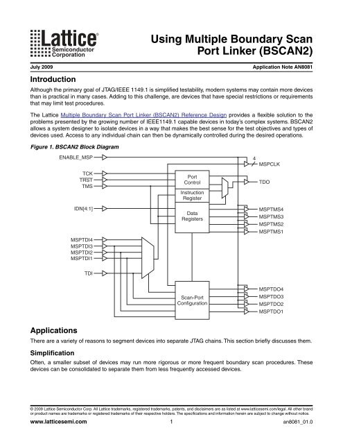
The <strong>Lattice</strong> Multiple Boundary Scan Port Linker (<strong>BSCAN2</strong>) Reference Design provides a flexible solution to the<br />
problems presented by the growing number of IEEE1149.1 capable devices in today’s complex systems. <strong>BSCAN2</strong><br />
allows a system designer to isolate devices in a way that makes the best sense for the test objectives and types of<br />
devices used. Access to any individual chain can then be dynamically controlled during the desired operations.<br />
Figure 1. <strong>BSCAN2</strong> Block Diagram<br />
Applications<br />
There are a variety of reasons to segment devices into separate JTAG chains. This section briefly discusses them.<br />
Simplification<br />
ENABLE_MSP<br />
TCK<br />
TRST<br />
TMS<br />
IDN[4:1]<br />
MSPTDI4<br />
MSPTDI3<br />
MSPTDI2<br />
MSPTDI1<br />
Often, a smaller subset of devices may run more rigorous or more frequent boundary scan procedures. These<br />
devices can be consolidated to separate them from less frequently accessed devices.<br />
© 2009 <strong>Lattice</strong> <strong>Semiconductor</strong> Corp. All <strong>Lattice</strong> trademarks, registered trademarks, patents, and disclaimers are as listed at www.latticesemi.com/legal. All other brand<br />
or product names are trademarks or registered trademarks of their respective holders. The specifications and information herein are subject to change without notice.<br />
www.latticesemi.com<br />
TDI<br />
Using Multiple Boundary Scan<br />
Port Linker (<strong>BSCAN2</strong>)<br />
1<br />
Port<br />
Control<br />
Instruction<br />
Register<br />
Data<br />
Registers<br />
Scan-Port<br />
Configuration<br />
4<br />
MSPCLK<br />
TDO<br />
MSPTMS4<br />
MSPTMS3<br />
MSPTMS2<br />
MSPTMS1<br />
MSPTDO4<br />
MSPTDO3<br />
MSPTDO2<br />
MSPTDO1<br />
an8081_01.0
Using Multiple Boundary Scan<br />
<strong>Lattice</strong> <strong>Semiconductor</strong> Port Linker (<strong>BSCAN2</strong>)<br />
Reduce the Need for Buffering<br />
As the number of devices in a JTAG chain increases, the signals that are distributed in parallel – TCK, TMS and<br />
TRST – require buffering to reduce the effects of fanout. Creating smaller sub-chains reduces this requirement.<br />
Additional I/O buffers can also be used for larger sub-chains to reproduce these signals.<br />
Mixed JTAG Voltages<br />
Handling multiple voltages in a JTAG chain involves careful consideration and often level translators. The flexible<br />
I/O banking structure of <strong>Lattice</strong> PLDs allows multiple I/O voltages within the same device. This allows the system<br />
designer to greatly simplify this task by placing only compatible voltage devices in each sub-chain.<br />
Removable Subsystems<br />
Modular systems ordinarily require separate JTAG chains or the presence of all daughter cards for boundary scan<br />
continuity. Partitioning each sub-chain according to a physical connector allows a flexible method to route around<br />
any portion of the system that is not currently present.<br />
JTAG Chain Faults<br />
The serial nature of JTAG signaling means that a faulty or physically damaged device can render the rest of the<br />
devices in the same chain inaccessible. By creating smaller sub-chains, a problem device can be routed around,<br />
leaving other sub-chains available. Other system testing can be performed in this case, allowing the ability to test<br />
other parts of the system for faults.<br />
Supply Separation<br />
During portions of boundary scan testing, some devices may be desired or required to be fully powered down.<br />
Since an unpowered device disrupts the JTAG chain, separating devices according to supply requirements allows a<br />
flexible solution for partially powered conditions.<br />
Custom Access Requirements<br />
Implementation in a PLD allows flexible configurations to suit custom requirements. It may be desirable to select<br />
between two master JTAG ports, or add provisions to connect to a sub-chain directly externally. By adding simple<br />
logic outside of the <strong>BSCAN2</strong> blocks, alternate access methods are easily achieved.<br />
Low-Speed Devices<br />
The overall TCK rate is limited to the lowest speed allowed by the slowest device in a chain. A device with a low<br />
TCK frequency specification may be a significant bottleneck in performance when other devices are capable of<br />
higher speeds. Partitioning slower devices into separate chains allows disabling of these devices to utilize a higher<br />
test speed for the remaining devices.<br />
Devices with Special Requirements<br />
Although most modern devices have no significant IEEE 1149.1 compliance issues, legacy or more obscure<br />
devices may be present in a system design that limit the capabilities of the overall JTAG chain. These devices can<br />
be isolated to allow a broader range of operation for fully compliant devices.<br />
An example of partitioning a JTAG chain is shown below in Figure 2. In this example, an FPGA, CPLD and an ASIC<br />
device comprise one 3.3V chain. A lower voltage 1.8V chain is assembled in a second, consisting of an ASIC and<br />
another FPGA. A third chain contains processor devices, specifically separated from other devices. The fourth and<br />
final chain in this example is used to isolate one ASIC device that has been determined to have some special<br />
requirements or restrictions.<br />
2
Using Multiple Boundary Scan<br />
<strong>Lattice</strong> <strong>Semiconductor</strong> Port Linker (<strong>BSCAN2</strong>)<br />
Figure 2. Example Chain Setup<br />
<strong>BSCAN2</strong><br />
JTAG<br />
Host<br />
After defining the chain partitions and connecting accordingly, the overall chain is now configurable through<br />
<strong>BSCAN2</strong> register control. Any combination of sub-chains can now be enabled. Figure 3 shows a simplified logical<br />
data path when all LSPs are active.<br />
Figure 3. All Ports Active<br />
<strong>BSCAN2</strong><br />
JTAG<br />
Host<br />
LSP1<br />
LSP2<br />
LSP3<br />
LSP4<br />
LSP1<br />
LSP2<br />
LSP3<br />
LSP4<br />
FPGA<br />
ASIC<br />
CPLD ASIC<br />
FPGA<br />
uP uP<br />
ASIC<br />
FPGA<br />
ASIC<br />
uP<br />
ASIC<br />
For situations where specific inclusion or exclusion of sub-chains is desired, the selection of sub-chains can be<br />
more specific. In the case of programming programmable logic devices, relevant sub-chains can be targeted, as<br />
3<br />
DSP<br />
Processor<br />
FPGA<br />
3.3V Chain<br />
1.8V Chain<br />
Processor Chain<br />
Special Device Chain<br />
CPLD ASIC<br />
uP<br />
DSP<br />
Processor
Using Multiple Boundary Scan<br />
<strong>Lattice</strong> <strong>Semiconductor</strong> Port Linker (<strong>BSCAN2</strong>)<br />
illustrated in Figure 4. In this case, the overall JTAG chain is routed around LSPs three and four, completely excluding<br />
them. The TAP controllers of each of the excluded devices remains in a constant state and no data is presented<br />
to them.<br />
Figure 4. Ports 1 and 2 Active<br />
<strong>BSCAN2</strong><br />
JTAG<br />
Host<br />
LSP1<br />
LSP2<br />
LSP3<br />
LSP4<br />
FPGA<br />
ASIC<br />
Some devices may have special requirements or have JTAG compliance issues that may disturb other, compliant<br />
devices. This problem is easily solved by selection of only the required sub-chain, as shown in Figure 5.<br />
4<br />
CPLD ASIC<br />
FPGA<br />
uP uP<br />
ASIC<br />
DSP<br />
Processor
Using Multiple Boundary Scan<br />
<strong>Lattice</strong> <strong>Semiconductor</strong> Port Linker (<strong>BSCAN2</strong>)<br />
Figure 5. Port 4 Active<br />
<strong>BSCAN2</strong><br />
JTAG<br />
Host<br />
LSP1<br />
LSP2<br />
LSP3<br />
LSP4<br />
FPGA<br />
ASIC<br />
5<br />
CPLD ASIC<br />
FPGA<br />
uP uP<br />
ASIC<br />
DSP<br />
Processor
Using Multiple Boundary Scan<br />
<strong>Lattice</strong> <strong>Semiconductor</strong> Port Linker (<strong>BSCAN2</strong>)<br />
It may be desirable to target some devices only when very specific conditions have been met. Examples of such<br />
devices are microprocessors and microcontrollers that maintain specific functions critical to vital operation of the<br />
system. It may be necessary in this case to put the system in a special state or operate from special power supplies<br />
before proceeding with a boundary scan or JTAG operation. In the example chain, this is shown as Figure 6, where<br />
LSP3 is selected.<br />
Figure 6. Port 3 Active<br />
<strong>BSCAN2</strong><br />
JTAG<br />
Host<br />
LSP1<br />
LSP2<br />
LSP3<br />
LSP4<br />
FPGA CPLD<br />
ASIC<br />
Although boundary scan is often used to perform thorough board-level connectivity tests with great efficiency, it<br />
relies on connectivity of all associated devices in a daisy-chain JTAG configuration. The potential vulnerability in<br />
this scheme is obvious when one device is physically damaged, defective, or installed incorrectly, affecting its JTAG<br />
port or associated logic. In this case, the malfunctioning device blocks the serial communication of otherwise valid<br />
boundary scan commands and data, rendering the test useless.<br />
By partitioning the JTAG devices into smaller sub-chains, the impact of this potential problem is reduced in two<br />
ways. First, the chains with proper JTAG continuity can be tested to their full extent, allowing valid boundary scan<br />
test information to be collected on the rest of the system. Second, it allows the same test methodology to narrow<br />
down which device is malfunctioning, aiding in troubleshooting efforts.<br />
The capability to route around a device’s non-functional JTAG circuitry is illustrated in Figure 7.<br />
ASIC<br />
uP<br />
ASIC<br />
6<br />
FPGA<br />
uP<br />
DSP<br />
Processor
Using Multiple Boundary Scan<br />
<strong>Lattice</strong> <strong>Semiconductor</strong> Port Linker (<strong>BSCAN2</strong>)<br />
Figure 7. Exclusion of a Non-Functioning Device<br />
Design Details<br />
<strong>BSCAN2</strong><br />
JTAG<br />
Host<br />
LSP1<br />
LSP2<br />
LSP3<br />
LSP4<br />
FPGA<br />
ASIC<br />
A more detailed diagram of the data path is illustrated in Figure 8. The conceptual multiplexing scheme as well as<br />
the latency of each LSP is shown. Each LSP, when enabled, adds one TCK cycle of latency before entering the<br />
local sub-chain. This flip-flop aids in meeting register-to-register timing for improved clock frequencies.<br />
One additional register exists at the end of the top_linker module. This register represents either its 8-bit instruction<br />
register, or one of the available data registers. A list of these register lengths is provided in Table 1.<br />
7<br />
CPLD ASIC<br />
FPGA<br />
uP uP<br />
ASIC<br />
DSP<br />
Processor
Using Multiple Boundary Scan<br />
<strong>Lattice</strong> <strong>Semiconductor</strong> Port Linker (<strong>BSCAN2</strong>)<br />
Figure 8. Simplified Functional Diagram of <strong>BSCAN2</strong> 4-Port top_linker Module<br />
TDI<br />
Table 1. <strong>BSCAN2</strong> Register Lengths<br />
tck<br />
Register 4-Port 8-Port Asset 8-Port JTAG<br />
1<br />
Instruction 8 8 8 + 8<br />
1<br />
Select 8 16 8 + 8<br />
1<br />
ID 4 4 4 + 4<br />
1<br />
Bypass 1 1 1 + 1<br />
1.1.8-Port JTAG model has two separate registers. The first is between LSP4 and LSP5, and the second after LSP8.<br />
tck<br />
tck<br />
tck<br />
tck<br />
<strong>BSCAN2</strong> Registers<br />
Instr Length = 8<br />
Bypass Length = 1<br />
The <strong>BSCAN2</strong> module is comprised of a central module named ‘top_linker’ and associated routing and connections<br />
to the device. Tristate buffers are not present within the ‘top_linker’ block to allow flexibility in connection of the signals.<br />
The most straight-forward connection is to simply bring the signals to the device I/O pins, as shown in Figure 9. The<br />
‘TDO_enable’ signal provides an output enable for TDO, allowing it to be active only in the Shift-IR and Shift-DR<br />
TAP controller states for IEEE1149.1 compliance.<br />
The 4-bit IDN bus provides an identification mechanism, allowing the JTAG host to confirm the presence of<br />
<strong>BSCAN2</strong>. This bus can be brought to I/O pins to set externally, or tied to a constant value at the instantiation of the<br />
‘top_linker’ module.<br />
8<br />
MSPTDO1<br />
LSP1<br />
MSPTDI1<br />
MSPTDO2<br />
LSP2<br />
MSPTDI2<br />
MSPTDO3<br />
LSP3<br />
MSPTDI3<br />
MSPTDO4<br />
LSP4<br />
MSPTDI4<br />
TDO
Using Multiple Boundary Scan<br />
<strong>Lattice</strong> <strong>Semiconductor</strong> Port Linker (<strong>BSCAN2</strong>)<br />
Figure 9. Instantiation Connections for <strong>BSCAN2</strong> top_linker Module<br />
Notes:<br />
1. Identification (IDN) inputs may be set from input pins or connected to hard-coded value in top_linker instantiation.<br />
2. TRST input optional. Tie to static high in top_linker instantiation to ignore the effects of this signal.<br />
3. ENABLE_MSP is optional. Driving this input low forces the MSP outputs to tristate, allowing an external device to control the lines.<br />
4. MSPTRST[] outputs are optional. If unused, these I/Os may be removed and the output from the top_linker module left open.<br />
Multiple ‘top_linker’ modules can be chained together to increase the number of available <strong>BSCAN2</strong> ports. This is<br />
accomplished by connecting TDO of one block to another’s TDI, as shown in Figure 10.<br />
Figure 10. Adding Ports by Chaining <strong>BSCAN2</strong> top_linker Modules<br />
TDI<br />
TCK<br />
TMS<br />
TRST<br />
Notes:<br />
1. Identification (IDN) inputs may be set from input pins or connected to hard-coded value in top_linker instantiation.<br />
2. Detailed MSP signal connections to LSPs not shown. Similar to instantiations of one top_linker block.<br />
3. TRST input optional. Tie to static high in top_linker instantiation to ignore the effects of this signal.<br />
4. TDO_enable output logically equivalent from each top_linker block.<br />
References<br />
ENABLE_MSP<br />
MSPTDI[4:1]<br />
IDN[4:1]<br />
TDI<br />
TCK<br />
TMS<br />
TRST<br />
TDI<br />
IDN<br />
MSPTDI[4:1]<br />
IDN[4:1]<br />
TDI<br />
TCK<br />
TMS<br />
TRST<br />
LSP1<br />
LSP2<br />
LSP3<br />
LSP4<br />
LSP5<br />
LSP6<br />
LSP7<br />
LSP8<br />
1 2 3 4 5 6 7 8<br />
top_linker<br />
TDO_enable<br />
<strong>BSCAN2</strong><br />
8-Port Block TDO<br />
(top_linker)<br />
TCK TMS<br />
TRST<br />
MSPTCK[4:1]<br />
MSPTMS[4:1]<br />
MSPTRST[4:1]<br />
MSPTDO[4:1]<br />
TDO_enable<br />
• RD1002, Multiple Boundary Scan Port Linker (<strong>BSCAN2</strong>) Reference Design<br />
• <strong>Lattice</strong> <strong>Semiconductor</strong> <strong>BSCAN2</strong> Webpage – www.latticesemi.com/products/intellectualproperty/referencedesigns/multipleboundaryscanportl.cfm<br />
9<br />
TDO<br />
LSP9<br />
LSP10<br />
LSP11<br />
LSP12<br />
LSP13<br />
LSP14<br />
LSP15<br />
LSP16<br />
1 2 3 4 5 6 7 8<br />
TDO_enable<br />
<strong>BSCAN2</strong><br />
TDI<br />
8-Port Block TDO<br />
IDN (top_linker)<br />
TCK TMS<br />
TRST<br />
MSPTCK[4:1]<br />
MSPTMS[4:1]<br />
MSPTRST[4:1]<br />
MSPTDO[4:1]<br />
TDO<br />
TDO
Using Multiple Boundary Scan<br />
<strong>Lattice</strong> <strong>Semiconductor</strong> Port Linker (<strong>BSCAN2</strong>)<br />
Third-Party Tools<br />
• Asset – www.asset-intertech.com<br />
• Corelis – www.corelis.com<br />
• JTAG Technologies – www.jtag.com<br />
Q & A<br />
Q: How many ports can be supported by <strong>BSCAN2</strong>?<br />
A: The pre-defined models support either 4 or 8 ports. Since the <strong>BSCAN2</strong> modules can be chained, larger implementations<br />
can be easily configured.<br />
Q: Can <strong>BSCAN2</strong> modules be cascaded?<br />
A: Yes. The <strong>BSCAN2</strong> modules can be connected to the LSP ports of other <strong>BSCAN2</strong> modules. This configuration is<br />
useful when there are multiple removable boards in a large system.<br />
Q: What is the 4-bit IDN input used for?<br />
A: This sets an identification register for the <strong>BSCAN2</strong> block. The JTAG host can query this register to ensure the<br />
<strong>BSCAN2</strong> function is present. The JTAG host software will require that you specify this value if this check is performed.<br />
Q: Are there any limitations of the number of devices supported by <strong>BSCAN2</strong>?<br />
A: There is no specific limit for the number of <strong>BSCAN2</strong> devices or number of JTAG devices attached to any LSP.<br />
Signal fanout should be controlled with buffering as necessary. JTAG host software may have limitations for memory<br />
or performance reasons. Check with the vendor for specific limits.<br />
Q: Can other unrelated logic be placed in the same PLD that implements <strong>BSCAN2</strong>?<br />
A: Yes. Other logic can be placed in the PLD, as long as it does not hinder the ability for <strong>BSCAN2</strong> to operate.<br />
Q: Can logic be added to <strong>BSCAN2</strong> within the PLD?<br />
A: Yes. Added logic, such as multiplexers and buffers can be added. Care should be taken to not impact the logical<br />
access of the JTAG host to <strong>BSCAN2</strong>. In the case of multiplexers, the path from the JTAG host to <strong>BSCAN2</strong> and its<br />
LSP connections should be configured when running the host software.<br />
Technical Support Assistance<br />
Hotline: 1-800-LATTICE (North America)<br />
+1-503-268-8001 (Outside North America)<br />
e-mail: techsupport@latticesemi.com<br />
Internet: www.latticesemi.com<br />
Revision History<br />
Date Version Change Summary<br />
July 2009 01.0 Initial release.<br />
10