Dispositivo apontador com interface USB usando ... - Bitbucket
Dispositivo apontador com interface USB usando ... - Bitbucket
Dispositivo apontador com interface USB usando ... - Bitbucket

Create successful ePaper yourself
Turn your PDF publications into a flip-book with our unique Google optimized e-Paper software.
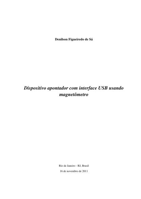
Denilson Figueiredo de Sá<br />
<strong>Dispositivo</strong> <strong>apontador</strong> <strong>com</strong> <strong>interface</strong> <strong>USB</strong> <strong>usando</strong><br />
magnetômetro<br />
Rio de Janeiro - RJ, Brasil<br />
16 de novembro de 2011
Denilson Figueiredo de Sá<br />
<strong>Dispositivo</strong> <strong>apontador</strong> <strong>com</strong> <strong>interface</strong> <strong>USB</strong> <strong>usando</strong><br />
magnetômetro<br />
Orientador:<br />
Nelson Quilula Vasconcelos<br />
Departamento de Ciência da Computação<br />
Instituto de Matemática<br />
Universidade Federal do Rio de Janeiro<br />
Rio de Janeiro - RJ, Brasil<br />
16 de novembro de 2011
<strong>Dispositivo</strong> <strong>apontador</strong> <strong>com</strong> <strong>interface</strong> <strong>USB</strong> <strong>usando</strong> magnetômetro<br />
Denilson Figueiredo de Sá<br />
Projeto Final de Curso submetido ao Departamento de Ciência da Computação do Instituto<br />
de Matemática da Universidade Federal do Rio de Janeiro <strong>com</strong>o parte dos requisitos necessários<br />
para obtenção do grau de Bacharel em Ciência da Computação.<br />
Apresentado por:<br />
Aprovado por:<br />
Denilson Figueiredo de Sá<br />
Prof. Nelson Quilula Vasconcelos<br />
Orientador<br />
Prof. Adriano Joaquim de Oliveira Cruz<br />
Prof a . Silvana Rossetto<br />
Rio de Janeiro - RJ, Brasil<br />
16 de novembro de 2011<br />
i
Agradecimentos<br />
Agradeço aos professores do DCC/UFRJ, em especial aos professores Nelson Quilula<br />
Vasconcelos, Adriano Joaquim de Oliveira Cruz, e Silvana Rossetto por participarem deste<br />
projeto, e aos professores João Carlos Pereira da Silva, Márcia Rosana Cerioli e Monique<br />
Moura Carmona pelo apoio durante esses anos de faculdade.<br />
Agradeço aos amigos de faculdade, em especial Alexandre Araújo Moreira, Luana Pinto<br />
Araújo e Priscila Neves Bilangieri por toda a paciência e apoio nos momentos em que mais<br />
precisei de ajuda.<br />
Agradeço também ao amigo de faculdade Bruno Bottino Ferreira pela paciência durante<br />
as semanas finais deste projeto.<br />
Agradeço aos amigos de trabalho, em especial Claudio Sá de Abreu e Marcelo Salhab<br />
Brogliato pelo apoio e pelo crescimento pessoal e profissional que me proporcionaram.<br />
ii
Resumo<br />
Este projeto tem <strong>com</strong>o objetivo implementar um dispositivo <strong>apontador</strong> <strong>com</strong>patível <strong>com</strong> um<br />
mouse <strong>USB</strong> utilizando um microcontrolador AVR ATmega8 de 8 bits e um magnetômetro. O<br />
dispositivo fruto deste projeto permite o usuário controlar o ponteiro do mouse movendo um<br />
sensor no ar, simplesmente apontando-o para a posição desejada na tela. É uma forma bastante<br />
intuitiva de controlar o ponteiro em situações onde um mouse não é adequado. Pode também ser<br />
usado para fins de acessibilidade, controlando o ponteiro através de movimentos da cabeça ou de<br />
qualquer outra parte do corpo.<br />
iii
Abstract<br />
This project implements a <strong>USB</strong> HID absolute pointing device using an ATmega8 AVR 8-bit<br />
microcontroller and a magnetometer. This device allows the user to control the mouse pointer by<br />
just moving a sensor in the air, pointing it to the desired screen position. It is a very intuitive<br />
way to control the pointer whenever it is not appropriate to use a mouse. It can also be used for<br />
accessibility, controlling the pointer by head movements, or movements of any other part of the<br />
body.<br />
iv
Lista de Figuras<br />
2.1 Fotos da PCB contendo o sensor . . . . . . . . . . . . . . . . . . . . . . . . p. 8<br />
2.2 Conectores do tipo A e do tipo B para <strong>USB</strong> 1.x/2.0 . . . . . . . . . . . . . . p. 9<br />
2.3 Topologia do barramento <strong>USB</strong> . . . . . . . . . . . . . . . . . . . . . . . . . p. 10<br />
3.1 Diagrama <strong>com</strong>pleto do circuito . . . . . . . . . . . . . . . . . . . . . . . . . p. 17<br />
4.1 Medições do sensor antes e depois da calibração do “zero” . . . . . . . . . . p. 36<br />
5.1 Visualização gráfica da saída do programa generate_sphere_vectors.py p. 39<br />
5.2 Exemplo de saída do programa draw_points.py . . . . . . . . . . . . . . . p. 40<br />
5.3 Definição dos vetores 3D . . . . . . . . . . . . . . . . . . . . . . . . . . . . p. 41<br />
5.4 As coordenadas 2D podem ser interpoladas a partir da projeção de P em cada<br />
borda . . . . . . . . . . . . . . . . . . . . . . . . . . . . . . . . . . . . . . p. 42<br />
5.5 O vetor P ′ é a <strong>com</strong>ponente de P contida no plano de A e B . . . . . . . . . . p. 43<br />
5.6 O vetor P pode ser representado <strong>com</strong>o A + x(B − A) + y(D − A) . . . . . . . . p. 45<br />
5.7 Os dois ângulos de abertura para os vetores de calibração . . . . . . . . . . . p. 46<br />
5.8 Cálculo exato de α . . . . . . . . . . . . . . . . . . . . . . . . . . . . . . . p. 46<br />
5.9 Razão entre ângulos . . . . . . . . . . . . . . . . . . . . . . . . . . . . . . . p. 47<br />
5.10 Razão entre distâncias . . . . . . . . . . . . . . . . . . . . . . . . . . . . . . p. 47<br />
5.11 Razão entre senos . . . . . . . . . . . . . . . . . . . . . . . . . . . . . . . . p. 47<br />
5.12 Razão entre cossenos . . . . . . . . . . . . . . . . . . . . . . . . . . . . . . p. 47<br />
5.13 Razão entre tangentes . . . . . . . . . . . . . . . . . . . . . . . . . . . . . . p. 47<br />
5.14 Sistema linear de 3 variáveis . . . . . . . . . . . . . . . . . . . . . . . . . . p. 48<br />
6.1 Fotos de uma PCB <strong>com</strong> cinco contatos disponíveis . . . . . . . . . . . . . . p. 51<br />
v
Lista de Siglas<br />
ADC Analog-to-Digital Converter . . . . . . . . . . . . . . . . . . . . . . . . . . . . . . . . . . . . . . . . . . . . . . . . 8<br />
API Application Programming Interface . . . . . . . . . . . . . . . . . . . . . . . . . . . . . . . . . . . . . . . . . 27<br />
DIP Dual In-line Package . . . . . . . . . . . . . . . . . . . . . . . . . . . . . . . . . . . . . . . . . . . . . . . . . . . . . . . 7<br />
EEPROM Electrically Erasable Programmable Read-Only Memory. . . . . . . . . . . . . . . . . . . . . . .7<br />
HID Human Interface Device . . . . . . . . . . . . . . . . . . . . . . . . . . . . . . . . . . . . . . . . . . . . . . . . . . . 12<br />
I 2 C Inter-Integrated Circuit . . . . . . . . . . . . . . . . . . . . . . . . . . . . . . . . . . . . . . . . . . . . . . . . . . . . . 8<br />
ISP In-System Programmer . . . . . . . . . . . . . . . . . . . . . . . . . . . . . . . . . . . . . . . . . . . . . . . . . . . . 16<br />
LCC Leaded Chip Carrier . . . . . . . . . . . . . . . . . . . . . . . . . . . . . . . . . . . . . . . . . . . . . . . . . . . . . . . 8<br />
LED Light-Emitting Diode . . . . . . . . . . . . . . . . . . . . . . . . . . . . . . . . . . . . . . . . . . . . . . . . . . . . . 16<br />
LKML Linux Kernel Mailing List . . . . . . . . . . . . . . . . . . . . . . . . . . . . . . . . . . . . . . . . . . . . . . . . . 33<br />
NRZI Non-Return-to-Zero Inverted . . . . . . . . . . . . . . . . . . . . . . . . . . . . . . . . . . . . . . . . . . . . . . . . 9<br />
PCB Printed Circuit Board. . . . . . . . . . . . . . . . . . . . . . . . . . . . . . . . . . . . . . . . . . . . . . . . . . . . . . .8<br />
PDIP Plastic Dual In-line Package . . . . . . . . . . . . . . . . . . . . . . . . . . . . . . . . . . . . . . . . . . . . . . . . 7<br />
QFN Quad-Flat No-leads Package . . . . . . . . . . . . . . . . . . . . . . . . . . . . . . . . . . . . . . . . . . . . . . . . 7<br />
QFP Quad Flat Package . . . . . . . . . . . . . . . . . . . . . . . . . . . . . . . . . . . . . . . . . . . . . . . . . . . . . . . . . 7<br />
SCL Serial Clock . . . . . . . . . . . . . . . . . . . . . . . . . . . . . . . . . . . . . . . . . . . . . . . . . . . . . . . . . . . . . . 13<br />
SDA Serial Data . . . . . . . . . . . . . . . . . . . . . . . . . . . . . . . . . . . . . . . . . . . . . . . . . . . . . . . . . . . . . . . 13<br />
SRAM Static Random-Access Memory . . . . . . . . . . . . . . . . . . . . . . . . . . . . . . . . . . . . . . . . . . . . . 7<br />
TWI Two-Wire Interface . . . . . . . . . . . . . . . . . . . . . . . . . . . . . . . . . . . . . . . . . . . . . . . . . . . . . . . . 8<br />
<strong>USB</strong>-IF <strong>USB</strong> Implementers’ Forum . . . . . . . . . . . . . . . . . . . . . . . . . . . . . . . . . . . . . . . . . . . . . . . . 28<br />
<strong>USB</strong> Universal Serial Bus . . . . . . . . . . . . . . . . . . . . . . . . . . . . . . . . . . . . . . . . . . . . . . . . . . . . . . . 9<br />
vi
Sumário<br />
1 Introdução p. 1<br />
1.1 Motivação e objetivos . . . . . . . . . . . . . . . . . . . . . . . . . . . . . . p. 2<br />
1.2 Trabalhos relacionados . . . . . . . . . . . . . . . . . . . . . . . . . . . . . p. 3<br />
1.2.1 Wiimote . . . . . . . . . . . . . . . . . . . . . . . . . . . . . . . . . p. 3<br />
1.2.2 SmartNav, TrackIR, HeadMouse . . . . . . . . . . . . . . . . . . . . p. 3<br />
1.2.3 Projetos baseados em acelerômetro . . . . . . . . . . . . . . . . . . p. 4<br />
1.3 Estrutura da monografia . . . . . . . . . . . . . . . . . . . . . . . . . . . . . p. 4<br />
2 Componentes e protocolos p. 6<br />
2.1 Microcontrolador ATmega8 . . . . . . . . . . . . . . . . . . . . . . . . . . . p. 7<br />
2.2 Sensor HMC5883L . . . . . . . . . . . . . . . . . . . . . . . . . . . . . . . p. 8<br />
2.3 <strong>USB</strong> . . . . . . . . . . . . . . . . . . . . . . . . . . . . . . . . . . . . . . . p. 9<br />
2.3.1 Endpoints . . . . . . . . . . . . . . . . . . . . . . . . . . . . . . . . p. 11<br />
2.4 <strong>USB</strong> HID . . . . . . . . . . . . . . . . . . . . . . . . . . . . . . . . . . . . p. 12<br />
2.5 I 2 C . . . . . . . . . . . . . . . . . . . . . . . . . . . . . . . . . . . . . . . . p. 13<br />
3 Descrição do hardware p. 15<br />
3.1 Visão geral do hardware . . . . . . . . . . . . . . . . . . . . . . . . . . . . p. 16<br />
3.2 Componentes ligados ao microcontrolador . . . . . . . . . . . . . . . . . . . p. 16<br />
3.3 Interface <strong>USB</strong> . . . . . . . . . . . . . . . . . . . . . . . . . . . . . . . . . . p. 18<br />
3.4 Interface <strong>com</strong> o sensor . . . . . . . . . . . . . . . . . . . . . . . . . . . . . p. 19<br />
3.4.1 Alimentação . . . . . . . . . . . . . . . . . . . . . . . . . . . . . . p. 19<br />
vii
3.4.2 Barramento I 2 C . . . . . . . . . . . . . . . . . . . . . . . . . . . . . p. 19<br />
4 Descrição do software p. 21<br />
4.1 Visão geral do software . . . . . . . . . . . . . . . . . . . . . . . . . . . . . p. 22<br />
4.2 Ambiente de desenvolvimento . . . . . . . . . . . . . . . . . . . . . . . . . p. 22<br />
4.3 Boot loader . . . . . . . . . . . . . . . . . . . . . . . . . . . . . . . . . . . p. 22<br />
4.4 Comunicação I 2 C/TWI . . . . . . . . . . . . . . . . . . . . . . . . . . . . . p. 24<br />
4.5 Comunicação <strong>com</strong> o sensor . . . . . . . . . . . . . . . . . . . . . . . . . . . p. 25<br />
4.5.1 Configuração do sensor . . . . . . . . . . . . . . . . . . . . . . . . . p. 26<br />
4.6 Driver V-<strong>USB</strong> . . . . . . . . . . . . . . . . . . . . . . . . . . . . . . . . . . p. 27<br />
4.6.1 Configuração do driver V-<strong>USB</strong> . . . . . . . . . . . . . . . . . . . . p. 27<br />
4.7 Teclado <strong>USB</strong> . . . . . . . . . . . . . . . . . . . . . . . . . . . . . . . . . . p. 28<br />
4.8 Menu de configuração . . . . . . . . . . . . . . . . . . . . . . . . . . . . . . p. 30<br />
4.9 Mouse <strong>USB</strong> . . . . . . . . . . . . . . . . . . . . . . . . . . . . . . . . . . . p. 31<br />
4.9.1 Suavização do movimento . . . . . . . . . . . . . . . . . . . . . . . p. 32<br />
4.9.2 Bug no kernel do Linux . . . . . . . . . . . . . . . . . . . . . . . . p. 33<br />
4.10 Outras funcionalidades . . . . . . . . . . . . . . . . . . . . . . . . . . . . . p. 34<br />
4.10.1 Debouncing dos botões . . . . . . . . . . . . . . . . . . . . . . . . . p. 34<br />
4.10.2 Gravar configurações na EEPROM . . . . . . . . . . . . . . . . . . . p. 34<br />
4.10.3 Calibração do “zero” do sensor . . . . . . . . . . . . . . . . . . . . . p. 35<br />
5 Transformação de coordenadas p. 37<br />
5.1 Ferramentas auxiliares . . . . . . . . . . . . . . . . . . . . . . . . . . . . . p. 38<br />
5.2 Transformação <strong>usando</strong> geometria . . . . . . . . . . . . . . . . . . . . . . . . p. 40<br />
5.3 Transformação <strong>usando</strong> sistema de equações lineares . . . . . . . . . . . . . . p. 44<br />
5.4 Resultados . . . . . . . . . . . . . . . . . . . . . . . . . . . . . . . . . . . . p. 45<br />
6 Conclusões p. 49<br />
viii
6.1 Resultados alcançados . . . . . . . . . . . . . . . . . . . . . . . . . . . . . p. 50<br />
6.2 Trabalhos futuros . . . . . . . . . . . . . . . . . . . . . . . . . . . . . . . . p. 51<br />
Referências Bibliográficas p. 52<br />
Apêndice A -- main.c p. 56<br />
Apêndice B -- buttons.h e buttons.c p. 64<br />
Apêndice C -- <strong>com</strong>mon.h p. 67<br />
Apêndice D -- int_eeprom.h e int_eeprom.c p. 68<br />
Apêndice E -- keyemu.h e keyemu.c p. 71<br />
Apêndice F -- menu.h e menu.c p. 77<br />
Apêndice G -- mouseemu.h e mouseemu.c p. 88<br />
Apêndice H -- sensor.h e sensor.c p. 93<br />
Apêndice I -- hardwareconfig.h e usbconfig.h p. 100<br />
Apêndice J -- Makefile p. 108<br />
Apêndice K -- generate_sphere_vectors.py p. 115<br />
Apêndice L -- convert_coordinates.py p. 118<br />
Apêndice M -- draw_points.py p. 126<br />
Apêndice N -- render_images.sh p. 129<br />
Anexo A -- ATmega8 datasheet p. 130<br />
Anexo B -- HMC5883L datasheet p. 152<br />
ix
Anexo C -- 3V Tips ’n Tricks p. 173<br />
Anexo D -- Bi-directional level shifter for I 2 C-bus and other systems p. 176<br />
Anexo E -- Level shifting techniques in I 2 C-bus design p. 182<br />
x
1 Introdução<br />
“The world is moving so fast these days that the man who says it can’t be done is generally<br />
1<br />
interrupted by someone doing it.”<br />
Elbert Green Hubbard<br />
Neste capítulo são apresentados a motivação e os objetivos deste projeto, uma lista de<br />
trabalhos relacionados e a estrutura da monografia.
1.1 Motivação e objetivos<br />
Este projeto apresenta uma implementação de um dispositivo <strong>USB</strong> do tipo absolute poin-<br />
ting device que pode ser utilizado para controlar o ponteiro do mouse na tela do <strong>com</strong>putador<br />
seguindo os movimentos de um sensor. Dentre outras aplicações, este dispositivo pode ser muito<br />
conveniente em apresentações que usem um <strong>com</strong>putador ligado a um projetor.<br />
O sensor empregado neste projeto é um magnetômetro, também conhecido <strong>com</strong>o bússola<br />
digital, o qual permite medir a direção e a intensidade do campo magnético. Desta forma, é<br />
possível saber a direção (em relação à Terra) para onde o sensor está sendo apontado. A partir<br />
dessa informação é calculada a posição desejada para o ponteiro do mouse.<br />
Todos os cálculos são realizados por um microcontrolador ATmega8, no qual também foi<br />
implementado o protocolo <strong>USB</strong> HID. Assim, o dispositivo fruto deste projeto pode ser usado<br />
em qualquer <strong>com</strong>putador sem a necessidade da instalação de drivers específicos no sistema<br />
operacional.<br />
A ideia para este projeto surgiu da apresentação “Google I/O 2011: The Secrets of Google<br />
Pac-Man: A Game Show”, na qual o palestrante Marcin Wichary utiliza um iPod touch 1 preso ao<br />
seu pulso para controlar um objeto no telão através dos movimentos de seu braço [1]. O software<br />
que rodava no iPod touch durante a palestra era uma página escrita em HTML5 e JavaScript,<br />
a qual se <strong>com</strong>unicava <strong>com</strong> um servidor NodeJS através de uma conexão Wi-Fi. Conforme ele<br />
movia seu braço, os dados do acelerômetro eram enviados para o servidor, que por sua vez os<br />
repassava para o <strong>com</strong>putador que estava ligado ao projetor.<br />
Um iPod touch é um equipamento bastante poderoso, mas também é relativamente grande e<br />
caro 2 . Não é muito prático deixar um dispositivo desse tamanho preso ao braço ou a qualquer<br />
outra parte do corpo. Além disso, não é possível controlar um <strong>com</strong>putador diretamente através<br />
dele, é necessário instalar tanto no iPod <strong>com</strong>o no <strong>com</strong>putador algum software específico para<br />
essa funcionalidade.<br />
Diante dessas observações este projeto foi iniciado, objetivando ser mais barato, menor e<br />
mais simples de usar.<br />
Uma vez concluído e posteriormente refinado, este projeto pode ser aplicado para diversos<br />
fins. Estas são algumas das aplicações possíveis:<br />
1 iPod touch é um reprodutor multimídia portátil bastante similar ao telefone celular iPhone, porém sem todos os<br />
recursos deste. O iPod touch possui um acelerômetro e um giroscópio embutidos, mas não possui um magnetômetro.<br />
2 R$ 729,00 no site do fabricante [2].<br />
2
• Pode ser utilizado durante apresentações, permitindo ao palestrante apontar regiões do<br />
telão através do gesto natural de se apontar <strong>com</strong> a mão.<br />
• Pode ser utilizado em situações onde um mouse não é viável, situações onde não há um<br />
apoio para um mouse convencional.<br />
• Pode ser utilizado em exposições interativas, entretenimento e jogos.<br />
• Pode ser utilizado por pessoas que não podem ou não conseguem movimentar um mouse.<br />
O pequeno sensor pode ser preso à cabeça ou qualquer outra parte do corpo.<br />
Todo o material desenvolvido neste projeto está também disponível online em repositórios<br />
Mercurial e Git:<br />
https://bitbucket.org/denilsonsa/atmega8-magnetometer-usb-mouse<br />
https://github.<strong>com</strong>/denilsonsa/atmega8-magnetometer-usb-mouse<br />
1.2 Trabalhos relacionados<br />
1.2.1 Wiimote<br />
Wiimote é o nome dado aos controles do vídeo-game Wii, fabricado pela Nintendo. É um<br />
controle sem fio <strong>com</strong> acelerômetro embutido, capaz de detectar movimentos, e também funciona<br />
<strong>com</strong>o um <strong>apontador</strong> dentro da <strong>interface</strong> do vídeo-game, bastando apontá-lo para a tela. Para<br />
isso, é necessário colocar acima ou abaixo da tela uma sensor bar, que nada mais é do que um<br />
conjunto de LEDs infravermelhos [3].<br />
Cada Wiimote possui uma câmera infravermelha na sua região frontal. A posição do ponteiro<br />
é calculada através da posição dos LEDs, capturada pela câmera do controle.<br />
O funcionamento esperado do dispositivo implementado neste projeto – controlar o ponteiro<br />
na tela simplesmente apontando um dispositivo de hardware para a posição desejada – é muito<br />
similar ao Wiimote, embora <strong>com</strong> tecnologias distintas.<br />
1.2.2 SmartNav, TrackIR, HeadMouse<br />
A empresa NaturalPoint criou um produto chamado SmartNav [4] para controlar o ponteiro<br />
do mouse através de gestos. O produto é <strong>com</strong>posto de uma câmera colocada acima do monitor e<br />
um software proprietário para Windows ou Mac OS X. A câmera possui LEDs infravermelhos<br />
3
embutidos e consegue captar os pontos onde essa luz foi refletida. O usuário deve colar um<br />
pequeno pedaço de papel reflexivo em sua cabeça, boné, ou qualquer outra parte do corpo. O<br />
software no <strong>com</strong>putador, então, processa a imagem da câmera e a transforma em movimentos do<br />
ponteiro do mouse.<br />
A mesma empresa também lançou um produto chamado TrackIR [5] que funciona de<br />
maneira similar, porém é voltado para o mercado de jogos. Neste caso, em vez de controlar o<br />
ponteiro do mouse, os movimentos da cabeça são enviados diretamente para o jogo, onde são<br />
traduzidos para movimentos da câmera virtual dentro do ambiente simulado. Para obter seis<br />
graus de liberdade nos movimentos, o usuário precisa colocar na cabeça uma armação contendo<br />
três pontos reflexivos ou três LEDs infravermelhos.<br />
Ambos os produtos exigem que o usuário fique na frente de uma câmera e exigem um<br />
software proprietário instalado e configurado na máquina. O produto TrackIR está à venda a<br />
partir de US$ 99,95, enquanto o SmartNav está à venda a partir de US$ 399,00<br />
A empresa Origin Instruments tem um produto chamado HeadMouse [6] cujo funcionamento<br />
é muito similar ao SmartNav, mas não requer nenhum software instalado. Esse produto se<br />
identifica <strong>com</strong>o um mouse <strong>USB</strong> e portanto funciona em qualquer sistema. Está à venda por<br />
US$ 995,00.<br />
1.2.3 Projetos baseados em acelerômetro<br />
WiSHABI [7] é um projeto de dispositivo sem fio <strong>USB</strong> que pode funcionar <strong>com</strong>o teclado ou<br />
mouse e faz leituras a partir de um acelerômetro. Foi implementado <strong>usando</strong> dois microcontrola-<br />
dores ATmega8.<br />
“<strong>USB</strong> Wireless Tilt Mouse + Minesweeper” [8] é um outro projeto de mouse sem fio baseado<br />
num acelerômetro. Utiliza microcontroladores ATmega32 ou ATmega644.<br />
TiltStick [9] é um projeto que implementa um joystick <strong>USB</strong> baseado em leituras de um<br />
acelerômetro.<br />
Em <strong>com</strong>um, todos esses projetos usam microcontroladores de 8 bits da família AVR e<br />
implementam um dispositivo <strong>USB</strong> HID através do driver V-<strong>USB</strong>.<br />
1.3 Estrutura da monografia<br />
O capítulo 2 descreve os <strong>com</strong>ponentes e protocolos usados para a realização deste trabalho.<br />
4
O capítulo 3 descreve o hardware do dispositivo.<br />
O capítulo 4 descreve o firmware (software) do dispositivo.<br />
O capítulo 5 descreve o problema de transformação de coordenadas, apresentando as aborda-<br />
gens experimentadas e seus resultados.<br />
O capítulo 6 apresenta as conclusões deste trabalho, <strong>com</strong> os resultados alcançados e as<br />
limitações encontradas, assim <strong>com</strong>o sugestões para trabalhos futuros.<br />
5
2 Componentes e protocolos<br />
“I loved music, and in my ninth year at MIT, I decided to buy a hi-fi set. I figured that all I<br />
needed to do was look at the specifications. So I bought what looked like the best one, turned it<br />
on, and turned it off in five minutes, the sound was so poor.”<br />
6<br />
Amar Gopal Bose<br />
Neste capítulo são apresentados o microcontrolador ATmega8 e o sensor HMC5883L, assim<br />
<strong>com</strong>o os protocolos <strong>USB</strong> e <strong>USB</strong> HID, usados na <strong>com</strong>unicação do microcontrolador <strong>com</strong> o<br />
<strong>com</strong>putador, e o protocolo I 2 C, usado na <strong>com</strong>unicação do microcontrolador <strong>com</strong> o sensor.
2.1 Microcontrolador ATmega8<br />
ATmega8 é um microcontrolador de 8 bits da família AVR, fabricado pela Atmel Corporation.<br />
Suas características principais são [10]:<br />
• Arquitetura Harvard, <strong>com</strong> espaços de endereçamento distintos para instruções e para<br />
variáveis.<br />
• 8192 bytes de memória Flash para guardar o programa.<br />
• 512 bytes de memória Electrically Erasable Programmable Read-Only Memory (EEPROM)<br />
para guardar parâmetros de configuração do programa.<br />
• 1024 bytes de memória Static Random-Access Memory (SRAM) volátil para as variáveis.<br />
• Voltagem de operação de 4,5V a 5,5V.<br />
• Clock máximo de 16MHz <strong>usando</strong> um cristal externo.<br />
• Interface de <strong>com</strong>unicação serial I 2 C/TWI.<br />
• Disponível no encapsulamento PDIP 1 de 28 pinos, assim <strong>com</strong>o QFP e QFN 2 de 32 pinos.<br />
A arquitetura dos processadores AVR foi projetada em conjunto <strong>com</strong> os desenvolvedores<br />
do <strong>com</strong>pilador de C da IAR Systems. Como consequência, o conjunto de instruções do AVR foi<br />
pensado de modo a minimizar o overhead durante a execução de programas que tenham sido<br />
escritos em linguagens de alto nível [11].<br />
Além disso, as instruções são executadas num pipeline de dois estágios, permitindo um<br />
desempenho máximo de uma instrução por ciclo de clock. Nem sempre esse desempenho é<br />
alcançado, pois algumas instruções (<strong>com</strong>o as que acessam a memória SRAM e os desvios)<br />
demoram pelo menos dois ciclos [10].<br />
Todas as instruções da arquitetura AVR ocupam 16 ou 32 bits (2 ou 4 bytes). Por esse motivo,<br />
a memória Flash é endereçada por words de 16 bits. Podemos dizer que o ATmega8 possui<br />
8192 bytes de memória Flash, ou de maneira equivalente, 4096 words. A memória SRAM e a<br />
memória EEPROM são endereçadas por bytes [10].<br />
1 O encapsulamento do tipo Plastic Dual In-line Package (PDIP), também chamado de Dual In-line Package<br />
(DIP), é o ideal para se trabalhar numa protoboard, pois o circuito integrado pode ser diretamente encaixado nela.<br />
2 Para o produto final, em ambiente de produção industrial, o ideal é usar um encapsulamento mais <strong>com</strong>pacto,<br />
<strong>com</strong>o Quad Flat Package (QFP) ou Quad-Flat No-leads Package (QFN)<br />
7
O microcontrolador ATmega8 inclui um módulo de <strong>com</strong>unicação serial Inter-Integrated<br />
Circuit (I 2 C), porém, para evitar problemas de patentes e licenças, a Atmel Corporation usa o<br />
nome Two-Wire Interface (TWI) para sua implementação dessa <strong>interface</strong> [12].<br />
Embora existam alguns modelos de microcontrolador AVR <strong>com</strong> controlador <strong>USB</strong> embutido<br />
[13], o microcontrolador ATmega8 usado neste projeto não possui nenhum tipo de hardware<br />
dedicado para essa função. Para tal, foi usado um driver que implementa o protocolo <strong>USB</strong> via<br />
software, diretamente no firmware do microcontrolador. Essa solução será descrita em mais<br />
detalhes na seção 4.6.<br />
2.2 Sensor HMC5883L<br />
HMC5883L é um magnetômetro fabricado pela Honeywell. Um magnetômetro é também<br />
conhecido <strong>com</strong>o “bússola digital” ou “bússola eletrônica”.<br />
Esse sensor trabalha de 2,16V a 3,6V e é capaz de medir a intensidade do campo magnético<br />
<strong>usando</strong> o efeito magnetorresistivo em três eixos perpendiculares (X, Y, Z) e converte essas<br />
medidas para um formato digital através de um Analog-to-Digital Converter (ADC) de 12 bits,<br />
chegando a uma precisão de 1 ◦ a 2 ◦ . Sua <strong>interface</strong> de <strong>com</strong>unicação é I 2 C [14].<br />
11mm × 11mm<br />
Figura 2.1: Fotos da PCB contendo o sensor<br />
O circuito integrado possui encapsulamento Leaded Chip Carrier (LCC) e tem apenas<br />
3,0 × 3,0 × 0,9mm de tamanho. É impossível trabalhar manualmente <strong>com</strong> algo tão minúsculo,<br />
por isso foi adquirida uma Printed Circuit Board (PCB) já contendo o sensor e alguns capacitores<br />
[15]. Essa placa possui quatro contatos, sendo metade deles para alimentação (GND e VDD) e a<br />
outra metade para <strong>com</strong>unicação I 2 C (SDA e SCL). Essa PCB pode ser vista na figura 2.1.<br />
8
2.3 <strong>USB</strong><br />
A partir do ano de 1994, as empresas Compaq, Hewlett-Packard, Intel, Lucent, Microsoft,<br />
NEC e Philips desenvolveram um protocolo chamado Universal Serial Bus (<strong>USB</strong>). Essa iniciativa<br />
foi motivada pela inexistência de um barramento bidirecional de baixo custo para periféricos<br />
de baixa e média velocidade. Além disso, a falta de flexibilidade dos barramentos até então<br />
existentes não permitia reutilizá-los para outros periféricos, pois eram projetados para usos<br />
bastante específicos [16].<br />
A primeira versão do <strong>USB</strong>, conhecida <strong>com</strong>o “<strong>USB</strong> 1.0”, foi oficialmente lançada em janeiro<br />
de 1996 e definiu duas velocidades: low speed (1,5Mbit/s) e full speed (12Mbit/s). Alguns<br />
anos depois, em setembro de 1998, foi lançada sua primeira revisão, “<strong>USB</strong> 1.1”, que resolveu<br />
alguns problemas da versão anterior mas não introduziu nenhuma mudança significativa.<br />
A primeira grande revisão do protocolo foi lançada em abril de 2000, <strong>com</strong> o nome de “<strong>USB</strong><br />
2.0”. Esta versão introduziu uma terceira velocidade – high speed (480Mbit/s) – mas manteve<br />
total <strong>com</strong>patibilidade <strong>com</strong> a revisão anterior do protocolo: dispositivos <strong>USB</strong> 1.x funcionam em<br />
hosts <strong>USB</strong> 2.0, e dispositivos <strong>USB</strong> 2.0 funcionam em hosts <strong>USB</strong> 1.x (porém limitados a full<br />
speed).<br />
Figura 2.2: Conectores do tipo A e do tipo B para <strong>USB</strong> 1.x/2.0<br />
Uma conexão <strong>USB</strong> é formada por quatro vias (conforme pode ser visto na figura 2.2), sendo<br />
duas para alimentação (VBUS = 5V e GND) e duas para <strong>com</strong>unicação (D+ e D-). Os dados são<br />
transmitidos <strong>usando</strong> a codificação Non-Return-to-Zero Inverted (NRZI) <strong>com</strong> bit stuffing (um<br />
“zero” é inserido após seis bits “um” consecutivos) [16] [17].<br />
A velocidade de um dispositivo é determinada por hardware, de acordo <strong>com</strong> a posição do<br />
resistor de pull-up 3 nas vias de dados. <strong>Dispositivo</strong>s low speed possuem um resistor de pull-up<br />
3 Resistores de pull-up ou de pull-down servem para manter uma via de dados num nível lógico conhecido<br />
enquanto nenhuma transferência ocorre. Normalmente possuem um valor relativamente alto (de 1,5kΩ a 10kΩ)<br />
para drenar pouca corrente. Um resistor de pull-up conecta a via ao VDD e a mantém no nível lógico 1, enquanto<br />
9
ligado ao D-, enquanto dispositivos full speed possuem um resistor de pull-up ligado ao D+. Se<br />
não há nenhum resistor de pull-up, assume-se que não há nenhum dispositivo conectado [16]<br />
[17].<br />
<strong>Dispositivo</strong>s high speed, introduzidos no <strong>USB</strong> 2.0, inicialmente se identificam <strong>com</strong>o full<br />
speed (<strong>com</strong> um resistor de pull-up ligado ao D+), mas removem o resistor após uma negociação<br />
realizada durante o <strong>USB</strong> reset, caso o host também suporte high speed. Caso contrário, o<br />
resistor será mantido e o dispositivo funcionará em full speed. Essa negociação incial permite a<br />
<strong>com</strong>patibilidade entre dispositivos <strong>USB</strong> 2.0 high speed e hosts <strong>USB</strong> 1.x [16] [17].<br />
Hub 2<br />
Host<br />
RootHub<br />
Hub 1<br />
Func<br />
Hub 3 Hub 4 Func<br />
Func<br />
Hub 5 Func<br />
Hub 6 Hub 7<br />
Host (Tier 1)<br />
Func<br />
Func<br />
Func<br />
Tier 2<br />
Tier 3<br />
Compound Device<br />
Tier 4<br />
Figura 2.3: Topologia do barramento <strong>USB</strong><br />
Tier 5<br />
Tier 6<br />
Tier 7<br />
A conexão de equipamentos <strong>USB</strong> segue uma topologia de estrela em camadas, que também<br />
pode ser entendida <strong>com</strong>o uma árvore (conforme figura 2.3). No centro da estrela (ou na raiz da<br />
árvore) temos obrigatoriamente o host, que normalmente é um <strong>com</strong>putador. Por definição, o<br />
host contém um root hub. Cada cabo <strong>USB</strong> é uma conexão ponto-a-ponto que liga um hub da<br />
camada imediatamente acima a um dispositivo na camada imediatamente abaixo. Um dispositivo<br />
pode ser um outro hub ou então uma função. Por limitações de tempo de propagação, o número<br />
máximo de camadas é sete, incluindo a camada que contém o host [16].<br />
A especificação <strong>USB</strong> define dois tipos de conectores (ilustrados na figura 2.2). Um cabo<br />
<strong>USB</strong> possui uma ponta de cada tipo, sendo que o plugue do tipo A é conectado ao hub da camada<br />
acima, e o plugue do tipo B é conectado ao dispositivo da camada abaixo. Posteriormente, foram<br />
um resistor de pull-down conecta a via ao GND e a mantém no nível lógico 0.<br />
10
também especificados conectores de tamanho mais reduzido (Mini e Micro), mas os conceitos<br />
continuam os mesmos.<br />
O protocolo de <strong>com</strong>unicação do <strong>USB</strong> pode ser entendido <strong>com</strong>o uma arquitetura master/slave,<br />
na qual o host é o master e os dispositivos têm o papel de slave. Só há um host por barramento<br />
<strong>USB</strong> e ele é responsável por iniciar e gerenciar cada transação. Como consequência, a maior<br />
parte da lógica está centralizada no host, simplificando bastante a implementação de dispositivos<br />
que se conectam ao barramento <strong>USB</strong> [17].<br />
Em novembro de 2008, foi lançada a especificação do <strong>USB</strong> 3.0, que introduziu uma quarta ve-<br />
locidade: super speed (5Gbit/s). A quantidade de mudanças para suportar essa nova velocidade<br />
é grande e foge do escopo deste trabalho.<br />
2.3.1 Endpoints<br />
Um endpoint pode ser visto <strong>com</strong>o um endereço lógico que pode receber dados do host ou<br />
enviar dados para ele. Todo dispositivo <strong>USB</strong> possui o endpoint 0, usado pelo próprio protocolo<br />
para mensagens de controle e de status [17].<br />
Além do endpoint 0, um dispositivo <strong>USB</strong> normalmente possui pelo menos mais um endpoint,<br />
usado para o objetivo fim do dispositivo.<br />
Control<br />
Há quatro tipos de endpoints: [17]<br />
Interrupt<br />
Bidirecional, usado durante a inicialização do dispositivo para <strong>com</strong>andos de controle do<br />
próprio protocolo <strong>USB</strong>.<br />
Unidirecional, latência garantida.<br />
Isochronous<br />
Bulk<br />
Unidirecional, latência e largura de banda garantidas, sem garantia de entrega, detecção de<br />
erros sem tentativa de reenvio. Apenas para dispositivos full speed e high speed.<br />
Unidirecional, sem garantia de latência ou de banda, porém <strong>com</strong> entrega garantida e<br />
recuperação de erros. Apenas para dispositivos full speed e high speed.<br />
Endpoints do tipo bulk são usados quando é importante transmitir dados corretamente, sem<br />
11
preocupação <strong>com</strong> o tempo necessário para concluir a transmissão. <strong>Dispositivo</strong>s de armazena-<br />
mento (<strong>com</strong>o pen drives) e scanners de fotos fazem uso deste tipo de endpoint.<br />
Endpoints do tipo isochronous são usados principalmente por dispositivos de streaming<br />
multimídia (audio e vídeo), nos quais há um fluxo constante de dados e o tempo de entrega é<br />
crítico.<br />
Endpoints do tipo interrupt são usados para notificar o host de eventos do dispositivo, ou<br />
para notificar o dispositivo a respeito de eventos do host. Normalmente são mensagens curtas.<br />
<strong>Dispositivo</strong>s de <strong>interface</strong> <strong>com</strong> o usuário, descritos na seção 2.4, fazem uso deste tipo de endpoint.<br />
Quando as mensagens são enviadas do host para o dispositivo, o endpoint é chamado de<br />
OUT. Quando são do dispositivo para o host, o endpoint é chamado de IN.<br />
É importante observar que um mesmo dispositivo pode ter múltiplos endpoints de tipos<br />
diferentes. Por exemplo, um scanner pode ter um endpoint do tipo bulk-in para transferir as<br />
imagens e um endpoint do tipo interrupt-in para notificar o host quando o botão do dispositivo é<br />
apertado.<br />
2.4 <strong>USB</strong> HID<br />
De modo a permitir a existência de dispositivos plug-and-play – que funcionam assim que<br />
são ligados ao host, sem necessidade de configurações feitas pelo usuário ou de instalação de<br />
drivers específicos – foram definidas algumas classes de dispositivos. Por exemplo, os populares<br />
pen drives, que substituíram os disquetes e CDs regraváveis para transferência de arquivos,<br />
pertencem à classe <strong>USB</strong> Mass Storage, e os sistemas operacionais modernos já incluem suporte<br />
nativo a dispositivos dessa classe.<br />
<strong>Dispositivo</strong>s de <strong>interface</strong> <strong>com</strong> seres humanos fazem parte da classe <strong>USB</strong> Human Interface<br />
Device (HID) e abrangem principalmente teclados, mouses e joysticks. No entanto, essa classe foi<br />
projetada de forma genérica e inclui outros tipos de dispositivos <strong>com</strong> necessidades similares, tais<br />
<strong>com</strong>o medidores de temperatura, controles de um painel (botões, alavancas, ajustes), volantes,<br />
pedais, leitores de códigos de barra, ou ainda novos dispositivos que não foram previstos<br />
inicialmente na especificação [18].<br />
A classe <strong>USB</strong> HID tem <strong>com</strong>o objetivos ser <strong>com</strong>pacta (para reduzir o espaço necessário<br />
no firmware do dispositivo), ser flexível e extensível, ser genérica e auto-descritiva (de modo<br />
que cada dispositivo descreva suas características de forma padronizada para o host). O driver<br />
da classe <strong>USB</strong> HID, presente no sistema operacional, é capaz de se <strong>com</strong>unicar <strong>com</strong> qualquer<br />
12
dispositivo dessa classe [18].<br />
Eventos do dispositivo (e.g., um botão foi pressionado ou o mouse foi movimentado) são<br />
enviados ao host através de um interrupt-in endpoint. Mensagens geradas pelo host e que devem<br />
ser enviadas para o dispositivo (e.g., acender ou apagar um dos indicadores do teclado) podem<br />
utilizar um interrupt-out endpoint ou o control endpoint [18].<br />
Essas mensagens enviadas ou recebidas pelo dispositivo são chamadas de reports. O formato<br />
delas é definido pelo próprio dispositivo, através do report descriptor, o qual é enviado ao host<br />
durante a negociação inicial do protocolo <strong>USB</strong> [18].<br />
A primeira versão da especificação do <strong>USB</strong> HID foi lançada em janeiro de 1996 (versão<br />
1.0). Sua primeira revisão ficou disponível em abril de 1999 (versão 1.1). Sua segunda revisão,<br />
que também é a mais recente, foi lançada em junho de 2001 (versão 1.11). Apesar desta<br />
versão ter sido lançada após o <strong>USB</strong> 2.0, a especificação do <strong>USB</strong> HID menciona apenas as duas<br />
velocidades de dispositivos presentes no <strong>USB</strong> 1.x, e incorretamente chama dispositivos full speed<br />
de high-speed [18].<br />
2.5 I 2 C<br />
Inter-Integrated Circuit (I 2 C) é um protocolo de <strong>com</strong>unicação serial bidirecional desenvol-<br />
vido em 1982 pela Philips Semiconductors (atual NXP Semiconductors). Foi projetado <strong>com</strong>o um<br />
protocolo simples e eficiente para <strong>com</strong>unicação entre circuitos integrados. Utiliza apenas duas<br />
vias: Serial Clock (SCL) e Serial Data (SDA) [19].<br />
A arquitetura do I 2 C é baseada no modelo master/slave, sendo que qualquer um dos disposi-<br />
tivos do barramento pode assumir o papel de master, e inclusive o papel pode mudar ao longo<br />
do tempo. O protocolo permite também múltiplos masters no mesmo barramento [19] [10]. No<br />
entanto, para este trabalho foi necessário apenas ligar dois dispositivos: o microcontrolador<br />
ATmega8 (funcionando sempre <strong>com</strong>o master) e o sensor HMC5883L (funcionando sempre <strong>com</strong>o<br />
slave).<br />
Tanto a via de dados SDA <strong>com</strong>o a via de clock SCL são bidirecionais. O master é responsável<br />
por gerar o sinal de clock, mas o dispositivo slave pode esticar o período de clock em determinadas<br />
situações, indicando que ainda não está pronto para responder [19].<br />
A <strong>com</strong>unicação no I 2 C é baseada em bytes. O master envia um sinal de START, seguido de<br />
um byte de endereço. Nesse byte, sete bits, indicam o endereço do slave e o oitavo bit indica o<br />
tipo de <strong>com</strong>unicação (escrita ou leitura). Após a transmissão desse byte, o master libera a linha<br />
13
de dados e o slave envia um bit zero durante próximo pulso de clock, sinalizando que recebeu o<br />
byte (acknowledge) [20].<br />
Logo após o byte de endereço, inicia-se a transmissão dos bytes de dados. Caso seja uma<br />
escrita, o master envia os bytes de dados exatamente da mesma forma <strong>com</strong>o enviou o byte de<br />
endereço, esperando pelo bit de acknowledge após cada byte enviado. Caso seja uma leitura, o<br />
master é responsável por gerar o clock (conforme já mencionado anteriormente), e o slave envia<br />
um bit a cada pulso do clock. Após cada oito bits recebidos (ou seja, após cada byte), o master<br />
deve enviar um bit de acknowledge para o slave. Em outras palavras, cada byte transmitido numa<br />
direção é sempre seguido de um bit de acknowledge transmitido na direção contrária [20].<br />
O master finaliza uma transmissão enviando um sinal STOP, ou então enviando um novo<br />
sinal START para iniciar uma nova transmissão imediatamente (condição conhecida <strong>com</strong>o<br />
REPEATED START) [10].<br />
Pode-se também observar que a quantidade total de bytes transferidos é uma escolha do<br />
master, e o slave não tem <strong>com</strong>o saber inicialmente quantos bytes serão requisitados.<br />
14
3 Descrição do hardware<br />
“It’s hardware that makes a machine fast. It’s software that makes a fast machine slow.”<br />
15<br />
Craig Bruce<br />
Neste capítulo são detalhados todos os <strong>com</strong>ponentes eletrônicos usados neste projeto.
3.1 Visão geral do hardware<br />
O núcleo do circuito é o microcontrolador ATmega8, o qual é responsável por ler os dados<br />
do sensor, fazer cálculos para converter os valores lidos, e enviar as coordenadas via <strong>USB</strong>.<br />
A seção 3.2 descreve <strong>com</strong>o todos os <strong>com</strong>ponentes são ligados ao microcontrolador.<br />
A seção 3.3 detalha a <strong>interface</strong> entre o microcontrolador e a porta <strong>USB</strong>.<br />
A seção 3.4 detalha a <strong>interface</strong> entre o microcontrolador e o sensor.<br />
Um diagrama do circuito <strong>com</strong>pleto pode ser visto na figura 3.1.<br />
3.2 Componentes ligados ao microcontrolador<br />
Um cristal de 12MHz, ligado aos pinos 9 e 10, define o clock do microcontrolador. O driver<br />
usado para a implementação do protocolo <strong>USB</strong>, descrito na seção 4.6, permite o uso de cristais<br />
de 12MHz, 15MHz, 16MHz ou 20MHz. A escolha pelo cristal de 12MHz foi arbitrária.<br />
O pino 1 (RESET) possui um resistor de pull-up (ligado ao VCC) e um botão ligado ao<br />
GND. Quando o botão é pressionado, o nível lógico do pino cai para zero e o microcontrolador é<br />
reiniciado. Esse botão de reset se mostrou bastante útil durante o desenvolvimento, mas não é<br />
necessário para o funcionamento deste projeto.<br />
Há três Light-Emitting Diodes (LEDs) ligados aos pinos 11, 12 e 13 (PORTD5, PORTD6,<br />
PORTD7), montados de modo a acender quando o valor lógico 1 é escrito. Foram usados para<br />
fins de depuração, mas não são essenciais para o funcionamento deste projeto.<br />
Há três botões ligados aos pinos 23, 24 e 25 (PORTC0, PORTC1, PORTC2), e ainda uma<br />
chave ligada ao pino 26 (PORTC3). Quando pressionados, o nível lógico de cada pino cai para<br />
zero. Cada pino possui internamente um resistor de pull-up, o qual foi habilitado pelo firmware,<br />
dispensando o uso de resistores externos.<br />
Os pinos 17, 18 e 19 (MOSI, MISO, SCK), juntamente <strong>com</strong> o pino 1 (RESET) são usados<br />
para In-System Programmer (ISP). Por simplicidade e por falta de necessidade, decidiu-se não<br />
usá-los para nenhuma outra função.<br />
Por fim, os pinos 2 e 4 (PD0 e PD2) estão ligados às vias <strong>USB</strong> D- e <strong>USB</strong> D+, e serão<br />
detalhados na seção 3.3; e os pinos 27 e 28 (SDA e SCL) estão ligados ao sensor através de um<br />
barramento I 2 C, e serão detalhados na seção 3.4.2.<br />
16
<strong>USB</strong> +5V<br />
10K Ω<br />
1K5 Ω<br />
D-<br />
D+<br />
470 Ω<br />
5V → 3.3V<br />
VCC GND<br />
1 2 3 4<br />
4.7µF<br />
68 Ω<br />
100nF<br />
22pF 12MHz<br />
22pF<br />
3V3<br />
3V6<br />
3V6<br />
+3.3V<br />
2K2 Ω<br />
2K2 Ω<br />
2K2 Ω<br />
68 Ω<br />
<strong>USB</strong> <strong>interface</strong><br />
GND<br />
VCC<br />
SDA<br />
Sensor<br />
SCL<br />
1 PC6<br />
(RESET)<br />
2 PD0<br />
(RXD)<br />
3 PD1<br />
(TXD)<br />
4 PD2<br />
(INT0)<br />
5 PD3<br />
(INT1)<br />
6 PD4<br />
(XCK/T0)<br />
7 VCC<br />
8 GND<br />
9 PB6<br />
10 PB7<br />
11 PD5<br />
12 PD6<br />
13 PD7<br />
14 PB0<br />
ATmega8<br />
(XTAL1/TOSC1)<br />
(XTAL2/TOSC2)<br />
(T1)<br />
(AIN0)<br />
(AIN1)<br />
(ICP1)<br />
2K2 Ω<br />
2K2 Ω<br />
+3.3V<br />
<strong>USB</strong> +5V<br />
+3.3V<br />
<strong>USB</strong> +5V<br />
PC5 28<br />
(ADC5/SCL)<br />
PC4 27<br />
(ADC4/SDA)<br />
PC3 26<br />
(ADC3)<br />
PC2 25<br />
(ADC2)<br />
PC1 24<br />
(ADC1)<br />
PC0 23<br />
(ADC0)<br />
GND 22<br />
AREF 21<br />
AVCC 20<br />
PB5 19<br />
(SCK)<br />
PB4 18<br />
(MISO)<br />
PB3 17<br />
(MOSI/OC2)<br />
PB2 16<br />
(SS/OC1B)<br />
PB1 15<br />
(OC1A)<br />
I²C Level-shifting<br />
G<br />
S D<br />
2K2 Ω<br />
I²C Level-shifting<br />
G<br />
S D<br />
2K2 Ω<br />
Figura 3.1: Diagrama <strong>com</strong>pleto do circuito<br />
<strong>USB</strong> +5V<br />
17
3.3 Interface <strong>USB</strong><br />
Uma porta <strong>USB</strong> fornece 5V na via VBUS, porém a especificação limita as vias de dados D+<br />
e D- ao intervalo de 2,8V a 3,6V [16].<br />
Uma solução seria usar um microcontrolador que possa funcionar a tensões mais baixas<br />
e colocar um circuito para reduzir a alimentação para dentro do intervalo desejado. Modelos<br />
mais recentes da linha AVR permitem o uso dessa solução [21]. No entanto, o microcontrolador<br />
ATmega8 usado neste projeto não trabalha <strong>com</strong> tensões inferiores a 4,5V [10].<br />
Uma outra solução é manter o microcontrolador alimentado <strong>com</strong> 5V e adicionar um circuito<br />
para reduzir a saída dos pinos do AVR para a tensão desejada. Esta foi a solução empregada<br />
neste projeto.<br />
O circuito usado para reduzir a tensão nas linhas de dados segue o mesmo esquema usado<br />
no projeto <strong>USB</strong>asp [22], também disponível no arquivo circuits/with-zener.png do driver<br />
V-<strong>USB</strong> [23]. É <strong>com</strong>posto de um diodo Zener de 3,6V ligando a linha de dados ao GND e um<br />
resistor de 68Ω entre o microcontrolador e o diodo Zener.<br />
Quando o microcontrolador escreve o nível lógico 1, seu pino sobe para 5V. Como essa<br />
tensão é maior que a tensão de ruptura do Zener, este <strong>com</strong>eça a conduzir, limitando a tensão<br />
da linha de dados. A diferença de 5 − 3,6 = 1,4V fica no resistor, resultando numa corrente de<br />
1,4V/68Ω = 20,6mA, que é abaixo do limite de 40mA para cada pino do microcontrolador<br />
[10].<br />
Além disso, conforme mencionado na seção 2.3, é preciso adicionar um resistor de pull-up à<br />
linha D-, indicando que este dispositivo é low speed. A especificação do <strong>USB</strong> 2.0 define que<br />
esse resistor deve ter 1,5kΩ [16]. O projeto <strong>USB</strong>asp, no entanto, usa um resistor de 2,2kΩ [22],<br />
que, mesmo fora da especificação, também funcionou.<br />
Por fim, para o funcionamento correto do driver V-<strong>USB</strong>, é necessário que a linha <strong>USB</strong> D+<br />
esteja ligada ao pino INT0 do microcontrolador. Além disso, é preciso que as duas vias de dados<br />
estejam ligadas a pinos que pertençam à mesma porta do microcontrolador [23]. Portanto, a<br />
linha D+ foi ligada ao pino 4 (PD2/INT0), e a linha D- foi ligada ao pino 2 (PD0).<br />
18
3.4 Interface <strong>com</strong> o sensor<br />
3.4.1 Alimentação<br />
O sensor HMC5883L trabalha <strong>com</strong> alimentação de 2,16V a 3,6V [14]. Como a <strong>USB</strong> fornece<br />
5V, é necessário adicionar um circuito para reduzir a tensão até um nível adequado.<br />
A solução aqui empregada utiliza um diodo Zener de 3,3V e um resistor de 470Ω [24]. É<br />
bastante similar àquela descrita na seção 3.3, mudando apenas os valores dos <strong>com</strong>ponentes.<br />
O diodo Zener e o resistor estão ligados em série entre VCC e GND, drenando constantemente<br />
uma corrente de (5V − 3,3V)/470Ω = 3,6mA e mantendo a tensão de 3,3V em relação ao GND<br />
entre esses dois <strong>com</strong>ponentes.<br />
Considerando que o sensor drena apenas 0,1mA quando em uso [14], a queda de tensão na<br />
alimentação quando em carga é desprezível, e portanto essa solução é bastante adequada para<br />
este propósito.<br />
3.4.2 Barramento I 2 C<br />
Se o microcontrolador e o sensor trabalhassem na mesma tensão, o barramento I 2 C seria<br />
apenas um par de fios ligando os pinos correspondentes dos dois <strong>com</strong>ponentes, e dois resistores<br />
de pull-up, um em cada fio.<br />
Todavia, os dois <strong>com</strong>ponentes não trabalham na mesma tensão. A primeira abordagem<br />
para este problema é verificar em suas especificações elétricas se as tensões de cada um estão<br />
dentro da faixa aceitável para o outro [25]. A tensão máxima de alimentação para o sensor é de<br />
3,6V [14], e tensão máxima tolerada no pino de alimentação é de 4,8V [14], que é abaixo da<br />
tensão de 5V do microcontrolador. Isso significa que não é prudente ligar os dois <strong>com</strong>ponentes<br />
diretamente.<br />
Neste caso, faz-se necessário adicionar um circuito para converter o nível lógico 1 entre 5V<br />
e 3,3V. Essa conversão precisa funcionar nas duas direções, pois o barramento é bidirecional.<br />
A solução adotada utiliza dois resistores de pull-up e um transistor MOSFET de canal<br />
N para cada uma das vias do barramento. É uma solução proposta pela própria Philips/NXP,<br />
desenvolvedora do padrão I 2 C [25] [26]. Vários modelos diferentes de transistor MOSFET<br />
podem ser usados para este fim. Neste projeto, foi usado o modelo 2N7000. Os resistores de<br />
pull-up usados foram de 2,2kΩ.<br />
19
Para entender <strong>com</strong>o essa solução funciona, é preciso analisá-la em três estados: [25] [26]<br />
Nenhum dos dois dispositivos está puxando o barramento para zero<br />
O lado de baixa tensão está em 3,3V devido ao resistor de pull-up. A diferença de potencial<br />
entre os terminais gate e source do transistor é zero, e portanto ele não está conduzindo.<br />
Desta forma, o lado de tensão mais alta está em 5V devido ao resistor de pull-up. Neste<br />
estado, os dois lados do barramento estão no nível lógico 1, apesar das tensões diferentes.<br />
O dispositivo de menor tensão está puxando o barramento para zero<br />
A diferença de potencial entre os terminais gate e source é 3,3V, e o transistor entra em<br />
condução. O lado de tensão mais alta é também puxado para zero, através do transistor em<br />
condução.<br />
O dispositivo de maior tensão está puxando o barramento para zero<br />
O lado de menor tensão é também puxado para baixo através do diodo interno do transistor<br />
MOSFET. Isso ocorre até que a diferença de potencial entre gate e source fique grande o<br />
suficiente, quando então o transistor entra em condução e o lado de menor tensão é puxado<br />
para zero através do transistor.<br />
20
4 Descrição do software<br />
21<br />
“Premature optimization is the root of all evil.”<br />
Donald Ervin Knuth<br />
Neste capítulo é detalhado o firmware deste projeto, assim <strong>com</strong>o o ambiente de desenvolvi-<br />
mento e algumas das dificuldades encontradas.
4.1 Visão geral do software<br />
Essencialmente, o trabalho do microcontrolador deste projeto é receber medições do sensor,<br />
aplicar um algoritmo de transformação de coordenadas e enviar para o <strong>com</strong>putador as novas<br />
coordenadas do ponteiro. Para que isso pudesse ser alcançado, o firmware foi dividido em três<br />
grandes partes.<br />
A primeira parte é a <strong>com</strong>unicação <strong>com</strong> o sensor, descrita nas seções 4.4 e 4.5.<br />
A segunda parte é transformar os medições do sensor em coordenadas na tela do <strong>com</strong>putador.<br />
Um estudo das diferentes abordagens para esse problema e seus resultados é apresentado no<br />
capítulo 5.<br />
A terceira parte é a <strong>com</strong>unicação <strong>com</strong> o <strong>com</strong>putador, alcançada através da implementação<br />
de um <strong>USB</strong> HID e descrita nas seções de 4.6 a 4.9.<br />
4.2 Ambiente de desenvolvimento<br />
O firmware deste projeto foi desenvolvido em ambiente Linux x86_64, utilizando o <strong>com</strong>pi-<br />
lador AVR-GCC versão 4.5.3, a biblioteca AVR-Libc versão 1.7.0 e as ferramentas do projeto<br />
Binutils versão 2.21.1. O código-fonte foi escrito na linguagem C e é facilmente portável para<br />
outros microcontroladores da família AVR. Para gravação do firmware no microcontrolador, foi<br />
usado o programa AVRDUDE.<br />
Todo o ambiente de desenvolvimento usado (AVR-GCC, Binutils, AVR-Libc, AVRDUDE) é<br />
<strong>com</strong>posto por software livre e está disponível para os principais sistemas operacionais (FreeBSD,<br />
Linux, Mac OS X e Windows) [27].<br />
O firmware deste projeto pode ser <strong>com</strong>pilado em qualquer sistema operacional que tenha as<br />
ferramentas citadas, mesmo em outras versões, embora alguns ajustes no Makefile possam ser<br />
necessários.<br />
4.3 Boot loader<br />
Durante o início do projeto, o ciclo de desenvolvimento podia ser resumido nestas etapas:<br />
1. Compilar o código-fonte.<br />
2. Desconectar a protoboard da <strong>USB</strong>.<br />
22
3. Conectar o gravador de AVR na <strong>USB</strong>.<br />
4. Gravar a nova versão do firmware.<br />
5. Desconectar o gravador de AVR.<br />
6. Reconectar a protoboard na <strong>USB</strong>.<br />
Rapidamente esse processo se mostrou bastante demorado e ineficiente, atrasando os testes<br />
e a depuração do código recém-escrito, e portanto atrasando o desenvolvimento. Além disso,<br />
também causava um desgaste mecânico desnecessário na porta <strong>USB</strong>. Embora esse desgaste seja<br />
desprezível a curto prazo, poderia se tornar um problema real para projetos de longo prazo.<br />
Visando agilizar e simplificar o ciclo de desenvolvimento, foi gravado um boot loader na<br />
região de boot do microcontrolador.<br />
Foi usado o <strong>USB</strong>aspLoader [28] <strong>com</strong>o boot loader. Ele foi escolhido por ser open source e<br />
por também usar o driver V-<strong>USB</strong>, o qual será descrito em mais detalhes na seção 4.6.<br />
Um boot loader é gravado nos endereços mais altos da memória Flash. O microcontrolador<br />
ATmega8 tem suporte a boot loaders de tamanhos 256, 512, 1024 e 2048 bytes [10]. Após<br />
<strong>com</strong>pilado, o <strong>USB</strong>aspLoader possui 2028 bytes, e portanto ocupa os 2048 bytes superiores da<br />
memória Flash.<br />
Logo após um reset, o ATmega8 normalmente <strong>com</strong>eçaria a execução do programa a partir<br />
do endereço mais baixo da memória. No entanto, quando se ativa o boot loader (através dos fuse<br />
bits do microcontrolador [10]), a execução <strong>com</strong>eça no endereço da região de boot.<br />
Portanto, ao iniciar o microcontrolador, o <strong>USB</strong>aspLoader é executado antes do firmware<br />
principal. Se uma determinada condição (configurável) for verdadeira, então o <strong>USB</strong>aspLoader<br />
assume o controle e se identifica <strong>com</strong>o um gravador <strong>USB</strong>asp 1 . Caso essa condição seja falsa<br />
(antes ou durante a execução do <strong>USB</strong>aspLoader), então o firmware principal é executado.<br />
Com o uso deste boot loader, o ciclo de desenvolvimento foi reduzido para:<br />
1. Compilar o código-fonte.<br />
2. Deixar ligada a chave conectada ao pino 26 (PORTC3) do microcontrolador.<br />
3. Apertar o botão de reset.<br />
1 <strong>USB</strong>asp é um gravador de AVR <strong>com</strong> conexão <strong>USB</strong> que é implementado <strong>usando</strong> um microcontrolador ATmega8<br />
ou similar [22].<br />
23
4. Gravar a nova versão do firmware.<br />
Após receber uma nova versão do firmware principal, o <strong>USB</strong>aspLoader automaticamente<br />
inicia a execução desse firmware recém-gravado.<br />
Com o uso de um boot loader, o ciclo de desenvolvimento tornou-se notavelmente mais<br />
rápido e dinâmico. Testar mudanças no firmware passou a ser fácil, e os testes se tornaram mais<br />
frequentes.<br />
Como desvantagem, o espaço disponível na memória Flash do microcontrolador foi reduzido<br />
de 8192 para 6144 bytes.<br />
4.4 Comunicação I 2 C/TWI<br />
O microcontrolador ATmega8 possui um hardware dedicado para <strong>com</strong>unicação I 2 C (cha-<br />
mada de TWI, conforme citado na seção 2.1). No entanto, seu uso é relativamente burocrático,<br />
tendo que implementar uma máquina de estados para gerenciar os registradores do módulo de<br />
TWI e a transmissão de dados [10]. O exemplo de código disponível na página 170 do datasheet<br />
do ATmega8 utiliza a técnica de busy-wait e não é adequado para o firmware deste projeto.<br />
De maneira geral, a técnica de busy-wait (espera ocupada) deve ser evitada porque bloqueia<br />
a execução do restante do código por tempo indeterminado, durante o qual nenhum tipo de<br />
trabalho útil pode ser realizado. Uma das possíveis consequências é causar um watchdog reset,<br />
reiniciando a execução do código do firmware. Além disso, a espera ocupada não garantiria que<br />
a função usbPoll() fosse chamada em intervalos menores que 50ms, conforme descrito na<br />
seção 4.6.1.<br />
Reconhecendo a dificuldade de usar esse módulo de maneira eficiente, a própria Atmel<br />
publicou um documento e o código-fonte de um driver 2 que utiliza o módulo TWI de maneira<br />
mais eficiente [20].<br />
Para este projeto, foi usado o driver disponível na application note “AVR315: Using the TWI<br />
module as I 2 C master”. Seu funcionamento é baseado em interrupções, e portanto pode realizar a<br />
transmissão de vários bytes de maneira assíncrona (não-bloqueante), uma característica altamente<br />
desejável. A rotina de tratamento da interrupção basicamente implementa uma máquina de<br />
estados [20].<br />
2 Neste contexto, “driver” significa um pedaço de software dentro do firmware que controla um módulo de<br />
hardware do microcontrolador. Não confundir <strong>com</strong> drivers do sistema operacional.<br />
24
O driver possui um buffer interno para armazenar os dados a serem enviados ou os dados<br />
sendo recebidos. O tamanho desse buffer é configurável em tempo de <strong>com</strong>pilação, através da<br />
linha:<br />
#define TWI_BUFFER_SIZE 7<br />
O código-fonte estava originalmente escrito para o <strong>com</strong>pilador IAR. Adaptá-lo para o<br />
<strong>com</strong>pilador GCC foi uma tarefa bastante simples, bastando apenas trocar os cabeçalhos e trocar<br />
a sintaxe da declaração da rotina de interrupção [29].<br />
// IAR:<br />
#include "ioavr.h"<br />
#include "inavr.h"<br />
// IAR syntax:<br />
#pragma vector=TWI_vect<br />
__interrupt void TWI_ISR(void)<br />
{<br />
...<br />
}<br />
4.5 Comunicação <strong>com</strong> o sensor<br />
// GCC:<br />
#include <br />
#include <br />
// GCC syntax:<br />
ISR(TWI_vect)<br />
{<br />
...<br />
}<br />
O sensor HMC5883L possui treze registradores de 8 bits que podem ser acessados pela<br />
<strong>com</strong>unicação serial, mais um registrador interno chamado de address pointer, o qual aponta para<br />
algum dos outros registradores e cujo valor não pode ser lido [14].<br />
Quando o master inicia uma escrita, o primeiro byte recebido pelo sensor é considerado o<br />
endereço de um registrador, e esse endereço é salvo no address pointer. Caso um segundo byte<br />
seja recebido, esse valor é salvo no registrador apontado pelo address pointer.<br />
Assim, para escrever num dos registradores de configuração do sensor, o firmware do<br />
microcontrolador prepara um vetor de três bytes: o endereço do sensor (juntamente <strong>com</strong> o bit que<br />
define uma operação de escrita), o número do registrador de configuração que será modificado, e<br />
o valor a ser escrito no registrador. Esse vetor é repassado ao driver de TWI (descrito na seção<br />
4.4), o qual copia esses bytes para um buffer interno e inicia a <strong>com</strong>unicação assincronamente.<br />
Quando o master inicia uma leitura, o sensor envia um byte <strong>com</strong> o valor contido no re-<br />
gistrador apontado pelo address pointer e incrementa o address pointer para apontar para o<br />
próximo registrador. Caso outro byte seja requisitado (ainda na mesma transmissão, ou em outra<br />
transmissão), o processo se repete, enviado o valor contido no registrador apontado pelo address<br />
25
pointer e incrementando-o. Desta forma, é possível ler o conteúdo de vários registradores<br />
adjacentes de maneira bem eficiente, <strong>com</strong> overhead de <strong>com</strong>unicação mínimo.<br />
No entanto, a implementação do sensor não é perfeita, e em certos casos o auto-incremento<br />
do address pointer não funciona <strong>com</strong>o esperado. Por exemplo, uma tentativa de ler todos os<br />
registradores (<strong>usando</strong> o auto-incremento para iterar automaticamente por todos eles) retorna<br />
valores diferentes (e inválidos) daqueles retornados por leituras individuais. De maneira geral, o<br />
auto-incremento funciona corretamente apenas para a leitura dos três registradores de identifica-<br />
ção do sensor e para a leitura dos seis registradores de dados, não atrapalhando o uso normal do<br />
sensor.<br />
Para ler os valores X, Y, Z do sensor, o microcontrolador <strong>com</strong>eça realizando uma escrita no<br />
sensor, enviando o valor 0x03 <strong>com</strong>o endereço do registrador. A seguir, realiza uma leitura de<br />
seis bytes consecutivos. Por fim, esses seis bytes lidos são convertidos numa struct de três<br />
variáveis inteiras de 16 bits.<br />
4.5.1 Configuração do sensor<br />
Durante a inicialização do firmware do microcontrolador, os registradores de configuração<br />
do sensor são escritos.<br />
O sensor foi configurado para atualizar os registradores de dados 75 vezes por segundo,<br />
sendo que cada valor é a média de oito amostras. O ganho do sensor foi configurado para ±1,3G,<br />
o que corresponde a 1090 bits por gauss 3 , ou 0,92mG por bit. Este ganho foi escolhido por<br />
permitir a maior precisão possível das medidas sem causar overflow no sensor.<br />
O sensor foi configurado para o modo de medição contínua, i.e., está continuamente medindo<br />
o campo magnético e atualizando os registradores de dados (75 vezes por segundo), mesmo que<br />
o microcontrolador não faça a leitura dessas medidas.<br />
Por limitação do sensor, o modo de medição contínua permite obter medições a uma taxa<br />
máxima de 75Hz. Apesar disso, é possível obter medições a até 160Hz se for configurado para<br />
o modo de medições individuais e o pino DRDY for monitorado [14]. Este pino normalmente<br />
fica no nível lógico 1, porém cai para 0 por 250µs assim que uma nova medida é colocada nos<br />
registradores de dados [14]. Portanto, seria possível ligar esse pino DRDY a algum dos pinos<br />
de interrupção do microcontrolador e escrever uma rotina que leia os dados e inicie a próxima<br />
medição.<br />
3 O símbolo G corresponde à unidade de densidade de fluxo magnético “gauss” [30]. O datasheet do sensor, no<br />
entanto, utiliza Ga <strong>com</strong>o símbolo para essa unidade.<br />
26
Todavia, a PCB usada neste projeto (figura 2.1) não possui um contato para o pino DRDY, e<br />
portanto não foi possível se aproveitar dessa técnica.<br />
4.6 Driver V-<strong>USB</strong><br />
O driver V-<strong>USB</strong> foi desenvolvido pela Objective Development Software GmbH. e é uma<br />
implementação em software do protocolo <strong>USB</strong>, funcionando em diversos microcontroladores da<br />
família AVR que não possuem um controlador <strong>USB</strong> embutido [23].<br />
Por ser implementado em software, o tempo de execução das rotinas do driver é crucial, e<br />
essas rotinas foram implementadas (pelos autores do driver) em assembly para clocks de 12MHz,<br />
15MHz, 16MHz ou 20MHz <strong>usando</strong> cristal, ou 12,8MHz ou 16,5MHz <strong>usando</strong> o oscilador<br />
interno do microcontrolador. Não é possível usar o driver <strong>com</strong> frequências diferentes destas<br />
[23].<br />
Apesar das rotinas internas estarem escritas em assembly, o driver disponibiliza uma<br />
Application Programming Interface (API) bastante simples em linguagem C.<br />
O driver implementa um dispositivo <strong>USB</strong> 1.1 low speed, mas possui algumas limitações.<br />
Uma delas é assumir que não há erros durante a <strong>com</strong>unicação, pois não há tempo de CPU<br />
suficiente para implementar checagem de erros via software. Além disso, as características<br />
elétricas dos pinos do microcontrolador não atendem estritamente a especificação <strong>USB</strong> [23].<br />
A especificação <strong>USB</strong> também define que os dispositivos devem implementar um modo<br />
suspend, no qual não devem consumir mais que 500µA [17]. O driver não implementa esse<br />
modo, mas explica em linhas gerais <strong>com</strong>o seria possível implementá-lo [23]. Para este projeto,<br />
não foi implementado o suporte ao modo suspend, pois não é uma tarefa trivial e está fora do<br />
escopo deste trabalho.<br />
Considerando as limitações citadas nos parágrafos anteriores, o dispositivo fruto deste<br />
projeto não é totalmente conformante <strong>com</strong> a especificação <strong>USB</strong>, mas isso não causou problemas<br />
nos <strong>com</strong>putadores onde o dispositivo foi testado, conforme resultados no capítulo 6. Além disso,<br />
essas limitações não impediram que mais de cem projetos tenham sido criados <strong>com</strong> sucesso [31].<br />
4.6.1 Configuração do driver V-<strong>USB</strong><br />
Toda a configuração do driver V-<strong>USB</strong> é feita no arquivo usbconfig.h. Como a maior parte<br />
da configuração é <strong>com</strong>partilhada <strong>com</strong> o boot loader, foi criado um arquivo hardwareconfig.h<br />
27
que contém as configurações <strong>com</strong>partilhadas entre o firmware principal e o boot loader (tais<br />
<strong>com</strong>o em quais pinos estão ligadas as linhas D- e D+), enquanto as configurações específicas<br />
foram mantidas no arquivo usbconfig.h.<br />
Para o firmware principal, foi habilitado um interrupt-in endpoint <strong>com</strong> intervalo polling de<br />
10ms (o menor valor possível para dispositivos low speed). Também foram definidos outros<br />
parâmetros, <strong>com</strong>o o nome do dispositivo, o nome do fabricante, o vendor-id e o product-id.<br />
Para um produto <strong>USB</strong> ser <strong>com</strong>ercializado, o fabricante precisa adquirir um vendor-id<br />
juntamente <strong>com</strong> o <strong>USB</strong> Implementers’ Forum (<strong>USB</strong>-IF), e pode escolher o product-id que<br />
quiser. Para projetos criados por hobby ou para fins acadêmicos, o custo e a burocracia para<br />
se adquirir tal número não é viável. 4 Portanto, para este projeto foi usado um par de vendor-<br />
id:product-id <strong>com</strong>partilhado pela Objective Development Software GmbH. 5 .<br />
Uma vez configurados os parâmetros necessários nos cabeçalhos do driver, usar sua API na<br />
linguagem C foi bastante simples. É necessário chamar a função usbInit() na inicialização<br />
do firmware, antes de habilitar as interrupções do microcontrolador, e é preciso chamar a<br />
função usbPoll() dentro do loop principal do firmware. É importante chamar essa função em<br />
intervalos menores que 50ms para que o driver funcione corretamente. Por fim, também foi<br />
necessário implementar a função usbFunctionSetup(), responsável por responder a algumas<br />
das mensagens recebidas no control endpoint 0 (as outras mensagens são respondidas diretamente<br />
pelo driver) [34].<br />
4.7 Teclado <strong>USB</strong><br />
Logo no início do projeto foi necessário testar se a <strong>com</strong>unicação <strong>USB</strong> estava funcionando<br />
corretamente, validando o software e o hardware. Além disso, embora alguns LEDs fossem<br />
suficientes para os testes iniciais de <strong>com</strong>unicação <strong>com</strong> o sensor, era preciso ter alguma forma de<br />
output para exibir os dados lidos.<br />
A solução foi implementar um teclado <strong>USB</strong> no microcontrolador. Essa implementação<br />
simula teclas sendo pressionadas de modo a escrever strings na tela do <strong>com</strong>putador. Em outras<br />
palavras, foi uma forma de se implementar o <strong>com</strong>ando print dentro do firmware.<br />
4 O logotipo <strong>USB</strong>, é uma marca registrada do <strong>USB</strong>-IF, e só pode ser usado em produtos que passaram nos testes<br />
dessa organização. [32] O custo para se adquirir um vendor-id é de pelo menos US$ 2.000,00 [33].<br />
5 Este projeto se identifica <strong>com</strong>o um dispositivo híbrido, funcionando ao mesmo tempo <strong>com</strong>o mouse e teclado.<br />
Não há nenhum par <strong>com</strong>partilhado de vendor-id:product-id que seja adequado a este projeto [23]. Após uma breve<br />
troca de e-mails <strong>com</strong> a Objective Development Software GmbH., e sabendo que o uso era para fins acadêmicos, foi<br />
sugerido usar valores quaisquer, aleatórios para esses campos.<br />
28
Teclados e mouses <strong>USB</strong> podem ser implementados <strong>com</strong>o dispositivos de boot. Tais dispositi-<br />
vos possuem um report descriptor predeterminado, definido no padrão <strong>USB</strong> HID. Isso foi criado<br />
para permitir o uso de teclados e mouses mesmo nos estágios iniciais do boot do <strong>com</strong>putador,<br />
quando pode ser inviável ter uma implementação <strong>com</strong>pleta da especificação HID [18].<br />
O protocolo boot obriga que o dispositivo se identifique ou <strong>com</strong>o um teclado ou <strong>com</strong>o<br />
um mouse, mas não <strong>com</strong>o os dois [18]. Além disso, ele define um report descriptor que<br />
suporta até seis teclas pressionadas simultaneamente, além das teclas modificadoras [18], o que<br />
é desnecessário para um teclado que vai apenas escrever strings. Por todos esses motivos, foi<br />
decidido implementar um teclado que não suporta o protocolo boot.<br />
O teclado implementado neste projeto utiliza o report descriptor mostrado na listagem 4.1,<br />
o qual foi baseado no projeto HIDKeys [35]. O código do report descriptor foi escrito utilizando<br />
a ferramenta HID Descriptor Tool [36], disponível no próprio site do <strong>USB</strong>-IF.<br />
0x05 , 0x01 , // USAGE_PAGE (Generic Desktop)<br />
0x09 , 0x06 , // USAGE (Keyboard)<br />
0xa1 , 0x01 , // COLLECTION (Application)<br />
0x85 , 0x01 , // REPORT_ID (1)<br />
// Modifier keys<br />
0x05 , 0x07 , // USAGE_PAGE (Keyboard)<br />
0x19 , 0xe0 , // USAGE_MINIMUM (Keyboard LeftControl)<br />
0x29 , 0xe7 , // USAGE_MAXIMUM (Keyboard Right GUI)<br />
0x15 , 0x00 , // LOGICAL_MINIMUM (0)<br />
0x25 , 0x01 , // LOGICAL_MAXIMUM (1)<br />
0x75 , 0x01 , // REPORT_SIZE (1)<br />
0x95 , 0x08 , // REPORT_COUNT (8)<br />
0x81 , 0x02 , // INPUT (Data ,Var ,Abs)<br />
// Normal keys<br />
0x05 , 0x07 , // USAGE_PAGE (Keyboard)<br />
0x19 , 0x00 , // USAGE_MINIMUM (Reserved (no event indicated))<br />
0x29 , 0x65 , // USAGE_MAXIMUM (Keyboard Application)<br />
0x15 , 0x00 , // LOGICAL_MINIMUM (0)<br />
0x25 , 0x65 , // LOGICAL_MAXIMUM (101)<br />
0x75 , 0x08 , // REPORT_SIZE (8)<br />
0x95 , 0x01 , // REPORT_COUNT (1)<br />
0x81 , 0x00 , // INPUT (Data ,Ary ,Abs)<br />
0xc0 , // END_COLLECTION<br />
Listagem 4.1: Report descriptor do teclado <strong>USB</strong><br />
O report usado por este teclado possui três bytes. O primeiro deles é o Report ID e tem valor<br />
1, identificando que este report corresponde ao report descriptor do teclado 6 . No segundo byte,<br />
cada um dos 8 bits corresponde a uma tecla modificadora, embora o firmware utilize apenas a<br />
tecla left shift. O terceiro byte é a tecla sendo pressionada.<br />
Internamente, o teclado virtual do microcontrolador possui um buffer de tamanho fixo que<br />
6 Na seção 4.9, o Report ID do mouse é definido <strong>com</strong> o valor 2.<br />
29
armazena a string a ser digitada, e um ponteiro indicando o próximo caractere do buffer que deve<br />
ser digitado. No loop principal do firmware, é checado se o interrupt-in endpoint está pronto<br />
para enviar dados. Se estiver, e houver algum caractere ainda não digitado, o firmware converte<br />
o caractere para o código da tecla correspondente e envia o report.<br />
Letras maiúsculas e alguns símbolos ligam o bit correspondente à tecla left shift, enquanto os<br />
outros caracteres desligam esse bit. Além disso, foi necessário detectar caracteres consecutivos<br />
que são convertidos para a mesma tecla (e.g., letras repetidas), e neste caso é enviado um report<br />
indicando nenhuma tecla pressionada antes de enviar o report correspondente ao caractere.<br />
A especificação <strong>USB</strong> HID Usage Tables define que o código de uma tecla mantém-se o<br />
mesmo, independente do que estiver impresso na tecla. Isto significa que a tecla “Z” de um<br />
teclado QWERTZ envia o mesmo código que a tecla “Y” de um teclado QWERTY [37]. Em<br />
outras palavras, a interpretação do código da tecla é de inteira responsabilidade do sistema<br />
operacional, através da configuração do layout do teclado. O teclado implementado neste projeto<br />
supõe estar configurado <strong>com</strong> layout US ou BR-ABNT2.<br />
Por fim, foram implementadas no firmware algumas funções para converter números inteiros<br />
em strings, seja na base decimal ou na base hexadecimal. Algumas dessas rotinas utilizam outras<br />
funções já implementadas na AVR-Libc.<br />
As rotinas do teclado <strong>USB</strong> foram usadas para fins de depuração e também <strong>com</strong>o base para o<br />
menu de configuração do dispositivo, descrito na seção 4.8.<br />
4.8 Menu de configuração<br />
Conforme mais funcionalidades estavam sendo implementadas no firmware (algumas delas<br />
para fins de depuração), a quantidade delas superou rapidamente o número de botões presentes<br />
no circuito. Como consequência, ficou cada vez mais difícil de adicionar outra funcionalidade<br />
ou mesmo usar as já existentes. Foi sentida a necessidade de uma <strong>interface</strong> melhor, mais prática<br />
e mais intuitiva para o uso do firmware.<br />
Essa foi a motivação para implementar um sistema de menus interativos. Esse sistema<br />
<strong>com</strong>bina o teclado virtual <strong>USB</strong> previamente implementado (descrito na seção 4.7) <strong>com</strong> os três<br />
botões presentes na protoboard (descritos na seção 3.1).<br />
Um dos botões foi escolhido para funcionar <strong>com</strong>o “confirma”, enquanto os outros dois<br />
funcionam <strong>com</strong>o “próximo item” e “item anterior”.<br />
O sistema de menus é iniciado apertando o botão “confirma”, o item atualmente selecionado<br />
30
é digitado na tela <strong>usando</strong> a funcionalidade do teclado <strong>USB</strong> (já descrito na seção 4.7). Todas as<br />
principais funcionalidades do firmware podem ser acessadas através dos menus, simplificando o<br />
uso do dispositivo (tanto para o usuário final quanto para o desenvolvedor).<br />
4.9 Mouse <strong>USB</strong><br />
O objetivo final deste projeto é controlar o ponteiro do mouse na tela do <strong>com</strong>putador, e para<br />
isso foi preciso implementar um mouse <strong>USB</strong> no microcontrolador de maneira similar ao teclado<br />
<strong>USB</strong> descrito na seção 4.7.<br />
Todavia, o mouse deste projeto tem uma diferença fundamental em relação aos mouses<br />
convencionais. A transformação de coordenadas, descrita no capítulo 5, obtém <strong>com</strong>o resultado<br />
um par de coordenadas (x,y) em relação à tela. Essas coordenadas são absolutas, no sentido<br />
de indicar uma posição específica da tela. Um mouse convencional, no entanto, detecta apenas<br />
movimentos e obtém coordenadas relativas (∆x,∆y), indicando a nova posição em relação à<br />
posição atual do ponteiro. Devido a essa diferença, o dispositivo implementado neste projeto é<br />
na verdade considerado um absolute pointing device 7 .<br />
A especificação <strong>USB</strong> HID define um report descriptor para mouses que implementem o<br />
protocolo boot [18]. Assim <strong>com</strong>o a implementação do teclado (seção 4.7), este dispositivo não<br />
tem suporte ao protocolo boot e utiliza o report descriptor mostrado na listagem 4.2.<br />
O report usado por este mouse possui seis bytes. O primeiro deles é o Report ID e tem valor<br />
2, identificando que este report corresponde ao report descriptor do mouse 8 . Os quatro bytes<br />
seguintes correspondem à posição (x,y), onde cada uma das duas coordenadas é representada<br />
por um número inteiro de 16 bits dentro do intervalo de 0 a 32767. Valores fora desse intervalo<br />
são considerados null values e devem ser ignorados pelo host [18]. O último byte representa os<br />
botões do mouse, sendo que os três bits menos significativos correspondem aos três botões, e os<br />
cinco bits restantes são ignorados.<br />
O algoritmo de transformação de coordenadas implementado no microcontrolador foi a<br />
abordagem <strong>usando</strong> um sistema de três equações lineares (seção 5.3). Essa solução foi escolhida<br />
por ser a mais simples e portanto ocupar pouco espaço na memória bastante limitada do micro-<br />
controlador 9 . Os cálculos utilizam variáveis float de 32 bits [38], e a resolução do sistema<br />
7 Apesar de na verdade ser um absolute pointing device, o nome mouse, por ser mais simples, mais curto e mais<br />
fácil de entender, é usado em todo o projeto.<br />
8 Na seção 4.7, o Report ID do teclado é definido <strong>com</strong> o valor 1.<br />
9 Outras abordagens mais <strong>com</strong>plexas podem ser implementadas caso microcontrolador ATmega8 seja substituído<br />
por outro <strong>com</strong> mais memória Flash.<br />
31
0x05 , 0x01 , // USAGE_PAGE (Generic Desktop)<br />
0x09 , 0x02 , // USAGE (Mouse)<br />
0xa1 , 0x01 , // COLLECTION (Application)<br />
0x85 , 0x02 , // REPORT_ID (2)<br />
0x09 , 0x01 , // USAGE (Pointer)<br />
0xa1 , 0x00 , // COLLECTION (Physical)<br />
// X, Y movement<br />
0x09 , 0x30 , // USAGE (X)<br />
0x09 , 0x31 , // USAGE (Y)<br />
0x15 , 0x00 , // LOGICAL_MINIMUM (0)<br />
0x26 , 0xff , 0x7f , // LOGICAL_MAXIMUM (32767)<br />
0x75 , 0x10 , // REPORT_SIZE (16)<br />
0x95 , 0x02 , // REPORT_COUNT (2)<br />
0x81 , 0x42 , // INPUT (Data ,Var ,Abs ,Null)<br />
0xc0 , // END_COLLECTION<br />
// Buttons<br />
0x05 , 0x09 , // USAGE_PAGE (Button)<br />
0x19 , 0x01 , // USAGE_MINIMUM (Button 1)<br />
0x29 , 0x03 , // USAGE_MAXIMUM (Button 3)<br />
0x15 , 0x00 , // LOGICAL_MINIMUM (0)<br />
0x25 , 0x01 , // LOGICAL_MAXIMUM (1)<br />
0x75 , 0x01 , // REPORT_SIZE (1)<br />
0x95 , 0x03 , // REPORT_COUNT (3)<br />
0x81 , 0x02 , // INPUT (Data ,Var ,Abs)<br />
// Padding for the buttons<br />
0x75 , 0x01 , // REPORT_SIZE (1)<br />
0x95 , 0x05 , // REPORT_COUNT (5)<br />
0x81 , 0x03 , // INPUT (Cnst ,Var ,Abs)<br />
0xc0 // END_COLLECTION<br />
linear utiliza o método de Gauss-Jordan [39].<br />
Listagem 4.2: Report descriptor do mouse <strong>USB</strong><br />
Para o funcionamento desse algoritmo de transformação de coordenadas é necessário primei-<br />
ramente calibrar os cantos da tela. Foi implementado um item no menu (seção 4.8) para essa<br />
finalidade.<br />
Do ponto de vista do usuário final, a calibração dos cantos é bastante simples. O usuário<br />
aponta o sensor na direção de um dos cantos e ativa o item do menu correspondente a esse<br />
canto. Nesse momento, é feita uma leitura do sensor, e o vetor lido é salvo na EEPROM e está<br />
imediatamente disponível para uso do algoritmo.<br />
4.9.1 Suavização do movimento<br />
O resultado do primeiro teste após a implementação do mouse <strong>USB</strong> e da transformação<br />
de coordenadas foi insatisfatório. Embora o algoritmo funcionasse corretamente e o ponteiro<br />
a<strong>com</strong>panhasse os movimentos do sensor, a posição do ponteiro não era estável. Mesmo <strong>com</strong> o<br />
32
sensor parado, o ponteiro oscilava significativamente na tela, indicando um ruído nas medições.<br />
Esse ruído pode ser consequência da interferência magnética de aparelhos elétricos e ele-<br />
trônicos, ou apenas uma limitação da precisão do sensor (que, conforme descrito na seção 2.2,<br />
possui um ADC de 12 bits). As razões exatas para tal ruído não são conhecidas.<br />
Foi então implementado um filtro de suavização de segunda ordem. O filtro é aplicado após<br />
a transformação de coordenadas, mas antes de preencher o report. O valor final das coordenadas<br />
na tela é uma média ponderada calculada desta forma:<br />
x ′ t = (1 − γ)x ′ t−1 + γxt<br />
x ′′<br />
t = (1 − γ)x ′′<br />
t−1 + γx′ t<br />
Onde xt é o resultado da transformação de coordenadas, x ′ t<br />
de primeira e segunda ordem, e x ′ t−1<br />
O valor final da coordenada x do ponteiro na tela é x ′′<br />
t<br />
coordenada y.<br />
e x′′<br />
t<br />
33<br />
são o resultado dos filtros<br />
e x′′<br />
t−1 são os resultados dos filtros após a medição anterior.<br />
. Um cálculo análogo é efetuado para a<br />
Experimentalmente foi escolhido γ = 0.125, considerando um balanço entre o tempo de<br />
resposta e a intensidade do filtro. Foi também observado que valores menores para γ, <strong>com</strong>o<br />
γ = 0.0625, introduziram um atraso perceptível para o usuário.<br />
4.9.2 Bug no kernel do Linux<br />
Durante os testes do mouse <strong>USB</strong>, foi descoberto um bug na implementação do suporte a<br />
<strong>USB</strong> HID no kernel do Linux.<br />
A especificação <strong>USB</strong> HID define que valores fora dos limites lógicos para um campo de<br />
um report devem ser ignorados [18]. Neste projeto, conforme descrito na seção 4.9, cada<br />
coordenada é representada por um inteiro de 16 bits dentro do intervalo de 0 a 32767. Valores<br />
fora desse intervalo, porém ainda representáveis em 16 bits, deveriam ser ignorados pelo sistema<br />
operacional. No entanto, foi observado que esses valores eram interpretados pelo sistema e<br />
causavam movimento indevido do ponteiro do mouse.<br />
O código do firmware foi então adaptado para não enviar valores fora desse intervalo. Não<br />
houve nenhuma perda de funcionalidade causada por essa adaptação.<br />
O bug foi reportado na Linux Kernel Mailing List (LKML) [40] e possivelmente será
corrigido na versão 3.3 ou posterior [41].<br />
4.10 Outras funcionalidades<br />
4.10.1 Debouncing dos botões<br />
Um problema bem conhecido na eletrônica é o fenômeno de bouncing. Botões são inerente-<br />
mente mecânicos, e, ao serem pressionados, demora uma fração de segundo até que o contato<br />
seja estabilizado. Isso ocorre devido às características elásticas dos materiais que os <strong>com</strong>põem.<br />
Nesse curto intervalo de tempo, o botão oscila rapidamente entre os estados de aberto e fechado.<br />
Conhecendo esse problema, faz-se necessário aplicar alguma técnica de debouncing. A<br />
solução empregada neste projeto foi inspirada na solução adotada pelo projeto TiltStick [9].<br />
Consiste em considerar a mudança de estado do botão apenas caso tenham-se passadas oito<br />
leituras consecutivas no novo estado. Isso foi implementado <strong>usando</strong> um byte para cada botão. A<br />
cada leitura, o valor do byte é deslocado um bit para a esquerda e a leitura atual é guardada no<br />
bit menos significativo. Caso o valor do byte seja igual a 0x00, considera-se que o botão não<br />
está pressionado. Caso o valor seja igual a 0xFF, considera-se que o botão está pressionado 10 .<br />
Qualquer outro valor é ignorado, e o botão mantém o estado anterior.<br />
4.10.2 Gravar configurações na EEPROM<br />
A biblioteca AVR-Libc já inclui funções para leitura e gravação de dados na EEPROM.<br />
Essas funções são implementadas <strong>usando</strong> a técnica de busy-wait, e portanto podem bloquear a<br />
execução do firmware por tanto tempo quanto demorar a leitura ou escrita dos bytes requisitados<br />
[42].<br />
O tempo total para a leitura de um byte da EEPROM no ATmega8 é de quatro ou cinco ciclos<br />
de clock 11 , enquanto a escrita de cada byte demora aproximadamente 8,5ms [10]. Portanto, a<br />
leitura é rápida o suficiente para não causar nenhum tipo de problema, mas a escrita é bastante<br />
demorada, e realizar escritas através da técnica de busy-wait não é adequado pelos mesmos<br />
motivos já citados na seção 4.4.<br />
Foi então necessário implementar um tipo de escrita não bloqueante. A própria Atmel<br />
10 No hardware, o nível lógico 0 representa um botão pressionado. Como é mais intuitivo pensar que 1 representa<br />
o botão pressionado e 0 botão solto, o valor lido pelo hardware é invertido pela rotina de leitura dos botões.<br />
11 O datasheet não é claro, informando que o acesso à EEPROM demora apenas um ciclo, mas também que a<br />
CPU fica parada por quatro ciclos antes que a instrução seguinte seja executada.<br />
34
publicou uma solução para esse problema na application note “AVR104: Buffered Interrupt<br />
Controlled EEPROM Writes” [43]. Sua implementação é bastante <strong>com</strong>pleta e inclui um buffer<br />
de escritas bastante poderoso, permitindo que múltiplas escritas para endereços arbitrários na<br />
EEPROM sejam empilhadas simultaneamente. Além disso, também tem suporte aos diferentes<br />
sleep modes do microcontrolador [10].<br />
Embora seja uma excelente solução para o caso geral, essa implementação é grande demais<br />
para as necessidades deste projeto. Sabendo que firmware não usa sleep modes e que não ocorrerá<br />
o caso de mais de uma gravação simultânea, foi possível simplificar bastante o código dessa<br />
implementação.<br />
Apenas um trecho da rotina de tratamento da interrupção foi aproveitada dessa application<br />
note, todo o restante foi reescrito ou simplesmente apagado. O código final empregado no<br />
firmware utiliza um buffer simples que permite gravar uma sequência de bytes numa posição<br />
contígua da EEPROM.<br />
4.10.3 Calibração do “zero” do sensor<br />
Durante o desenvolvimento do projeto foi observado que os vetores correspondentes às<br />
medições do campo magnético estavam enviesados, i.e., não eram centralizados ao redor das<br />
coordenadas (0,0,0).<br />
Não se sabe se esse efeito é uma característica intrínseca do sensor, ou se é causado por<br />
fatores externos. O datasheet do sensor tem algumas re<strong>com</strong>endações sobre o projeto da PCB<br />
na qual o sensor será montado. Em especial, re<strong>com</strong>enda afastar <strong>com</strong>ponentes que contenham<br />
materiais ferrosos, assim <strong>com</strong>o evitar trilhas condutoras embaixo ou próximo do sensor [14].<br />
Não foi possível descobrir se o fabricante da PCB adquirida (figura 2.1 na seção 2.2) tomou tais<br />
precauções.<br />
Para resolver esse problema, foi implementado um item no menu para a calibração do “zero”<br />
do sensor. Durante a calibração, o sensor deve ser movido em todas as direções, de modo a<br />
descobrir os valores máximo e mínimo para cada um dos eixos. Uma vez concluída a calibração,<br />
o viés é calculado <strong>com</strong>o a média entre os valores máximo e o mínimo, e é então gravado na<br />
EEPROM. Após calibrado, todas as leituras do sensor são <strong>com</strong>pensadas via software, <strong>usando</strong> o<br />
valor calibrado. O resultado pode ser visto na figura 4.1.<br />
35
300<br />
200<br />
100<br />
0<br />
100<br />
200<br />
300<br />
300 200 100 0 100 200 300<br />
300 200 100 0 100 200 300<br />
Figura 4.1: Medições do sensor antes e depois da calibração do “zero”<br />
300<br />
200<br />
100<br />
0<br />
100<br />
200<br />
300<br />
36
5 Transformação de coordenadas<br />
“Models are a bunch of equations; physics is what happens when you drop a hammer on your<br />
37<br />
big toe. They are not the same. Just ask your big toe.”<br />
Ken Matusow<br />
Neste capítulo é apresentado o problema de transformação de coordenadas, as abordagens<br />
experimentadas e os resultados observados em cada abordagem.
5.1 Ferramentas auxiliares<br />
O principal desafio teórico deste projeto foi transformar os vetores tridimensionais lidos do<br />
sensor em coordenadas bidimensionais na tela do <strong>com</strong>putador. Não existe uma única solução<br />
para este problema e foi preciso explorar algumas abordagens antes de decidir qual delas seria<br />
implementada no microcontrolador.<br />
Com o objetivo de experimentar e avaliar as diferentes abordagens para a transformação<br />
de coordenadas, foram desenvolvidas algumas ferramentas na linguagem Python. A escolha<br />
da linguagem foi motivada pela facilidade e rapidez de se escrever protótipos e pela extensa e<br />
abrangente biblioteca disponível.<br />
A primeira ferramenta foi chamada de generate_sphere_vectors.py e serve para simu-<br />
lar leituras do sensor. Esta ferramenta imprime na saída padrão uma lista de vetores 3D que<br />
cobrem pouco menos da metade da superfície de uma esfera. Também imprime quatro vetores<br />
correspondentes aos cantos da tela, os quais são usados nos cálculos explicados nas seções 5.2 e<br />
5.3. A listagem 5.1 mostra um trecho da saída desta ferramenta.<br />
topleft<br />
172 69 75<br />
topright<br />
172 -69 75<br />
bottomright<br />
172 -69 -75<br />
bottomleft<br />
172 69 -75<br />
0 141 141<br />
2 141 141<br />
5 141 141<br />
7 141 141<br />
10 141 141<br />
Listagem 5.1: Primeiras linhas da saída do programa generate_sphere_vectors.py<br />
A figura 5.1 mostra um gráfico dos vetores 3D impressos por esta ferramenta. Esse gráfico<br />
corresponde à região de −90 ◦ a 90 ◦ de longitude e −45 ◦ a 45 ◦ de latitude. Há um espaçamento<br />
de 1 ◦ de longitude e 2 ◦ de latitude entre os vetores.<br />
A segunda ferramenta foi chamada de convert_coordinates.py e implementa os algorit-<br />
mos de transformação de coordenadas explicados nas seções 5.2 e 5.3. Esta ferramenta lê vetores<br />
3D a partir da entrada padrão e imprime na saída padrão as coordenadas 2D correspondentes,<br />
calculadas de acordo <strong>com</strong> o algoritmo selecionado. Um exemplo de entrada e saída para esta<br />
ferramenta pode ser visto na listagem 5.2<br />
38
Figura 5.1: Visualização gráfica da saída do programa generate_sphere_vectors.py<br />
topleft<br />
172 69 75<br />
topright<br />
172 -69 75<br />
bottomright<br />
172 -69 -75<br />
bottomleft<br />
172 69 -75<br />
198 24 -3 0.348924 0.517374<br />
198 -3 24 0.518884 0.36101<br />
190 -44 45 0.788635 0.228421<br />
Listagem 5.2: Entrada para o programa convert_coordinates.py e a saída correspondente<br />
A terceira ferramenta foi chamada de draw_points.py e serve para visualizar graficamente<br />
as coordenadas 2D. Esta ferramenta desenha um ponto na tela para cada par de coordenadas lido<br />
da entrada padrão. A figura 5.2 mostra a saída desta ferramenta para os três pontos da listagem<br />
5.2.<br />
Essas três ferramentas podem ser usadas separadamente ou encadeadas através de um<br />
pipeline 1 .<br />
1 Pipeline significa ligar a saída padrão de um programa à entrada padrão do programa seguinte.<br />
39
Figura 5.2: Exemplo de saída do programa draw_points.py<br />
5.2 Transformação <strong>usando</strong> geometria<br />
Para esta abordagem é necessário calibrar os quatro cantos da tela, i.e., definir quatro vetores<br />
no espaço tais que:<br />
• O vetor A aponta na direção do canto superior esquerdo da tela.<br />
• O vetor B aponta na direção do canto superior direito da tela.<br />
• O vetor C aponta na direção do canto inferior direito da tela.<br />
• O vetor D aponta na direção do canto inferior esquerdo da tela.<br />
Também é definido o vetor P <strong>com</strong>o sendo a direção apontada pelo usuário. O objetivo da<br />
transformação de coordenadas é mapear o vetor P em coordenadas (x,y) contidas no plano da tela<br />
do <strong>com</strong>putador. As magnitudes dos vetores não são importantes, apenas a direção é considerada.<br />
Todos esses vetores podem ser vistos na figura 5.3<br />
Uma vez definido o problema, a etapa seguinte foi quebrá-lo em subproblemas. Em vez<br />
de tentar calcular diretamente as coordenadas 2D relativas ao vetor P, calcula-se a projeção de<br />
P em cada uma das bordas da tela, para a seguir interpolar as coordenadas (x,y) a partir das<br />
bordas, conforme a figura 5.4. Essa decisão foi tomada porque o quadrilátero ABCD não é<br />
necessariamente um retângulo.<br />
Para calcular essa projeção de P, primeiramente calcula-se o vetor unitário N (5.1), normal<br />
ao plano de A e B. São então calculados PN (5.2), a <strong>com</strong>ponente de P paralela ao vetor N; e P ′<br />
(5.3), a <strong>com</strong>ponente de P contida no plano de A e B. Isso é ilustrado na figura 5.5.<br />
40
D<br />
A B<br />
Figura 5.3: Definição dos vetores 3D<br />
N =<br />
A × B<br />
||A × B||<br />
P<br />
C<br />
41<br />
(5.1)<br />
PN = (N · P)N (5.2)<br />
P ′ = P − PN<br />
(5.3)<br />
Uma vez tendo P ′ , a etapa final é calcular sua posição na borda delimitada por A e B. Essa<br />
posição é definida <strong>com</strong>o um escalar α entre 0 e 1, sendo que 0 indica que P ′ é coincidente <strong>com</strong> o<br />
vetor A, e 1 indica que P ′ é coincidente <strong>com</strong> o vetor B. Valores fora desse intervalo indicam que<br />
P ′ está fora do setor angular delimitado por A e B.<br />
Como A, B e P ′ estão no mesmo plano, o valor exato de α pode ser calculado através de um<br />
sistema linear de duas variáveis α e β, o qual pode ser representado <strong>com</strong> a equação vetorial (5.4).<br />
A + α(B − A) = βP ′<br />
(5.4)<br />
As bases do espaço bidimensional correspondente ao plano dos vetores A, B e P ′ podem<br />
ser definidas <strong>com</strong>o os vetores X e Y ortonormais (5.5). Todos os pontos desse plano podem ser<br />
representados por uma <strong>com</strong>binação linear entre os vetores X e Y.
D<br />
A B<br />
Figura 5.4: As coordenadas 2D podem ser interpoladas a partir da projeção de P em cada borda<br />
X = A<br />
||A||<br />
A × N<br />
Y =<br />
||A × N||<br />
P<br />
C<br />
42<br />
(5.5)<br />
Definidas as bases do espaço bidimensional, as <strong>com</strong>ponentes de A, (B− A) e P ′ nesse espaço<br />
podem ser calculadas <strong>usando</strong> produto interno. (5.6)<br />
AX = A · X AY = A · Y (5.6)<br />
(B − A)X = (B − A) · X (B − A)Y = (B − A) · Y<br />
P ′ X = P′ · X P ′ Y = P′ · Y<br />
A equação vetorial (5.4) pode ser reescrita <strong>com</strong>o duas equações escalares (5.7), utilizando<br />
as <strong>com</strong>ponentes definidas em (5.6).<br />
AX + α(B − A)X = βP ′ X<br />
AY + α(B − A)Y = βP ′ Y<br />
(5.7)
N<br />
Figura 5.5: O vetor P ′ é a <strong>com</strong>ponente de P contida no plano de A e B<br />
Por fim, resolvendo o sistema linear definido em (5.4) e (5.7), obtemos o valor exato de α<br />
correspondente a uma das bordas da tela.<br />
Repetindo os cálculos para as outras bordas, podemos calcular (x,y) através de uma interpo-<br />
lação linear (5.8).<br />
onde<br />
A<br />
P<br />
P'<br />
B<br />
x(y) = y(DC − AB) + AB (5.8)<br />
y(x) = x(BC − AD) + AD<br />
x =<br />
AD(DC − AB) + AB<br />
1 − (BC − AD)(DC − AB)<br />
AB, BC, DC, AD = valor de α para cada borda<br />
Além do cálculo do valor exato de α, também foram experimentados cálculos aproximados<br />
para α, <strong>usando</strong> razão entre ângulos (5.9), razão entre distâncias (5.10), razão entre senos (5.11),<br />
razão entre cossenos (5.12), razão entre tangentes (5.13). Os resultados de cada abordagem estão<br />
listados na seção 5.4.<br />
43
α = ang(A, P′ )<br />
ang(A, B)<br />
�<br />
�<br />
� A P′<br />
�<br />
� −<br />
|A| |P<br />
α =<br />
′ �<br />
�<br />
�<br />
�<br />
| �<br />
�<br />
�<br />
�<br />
� A B �<br />
�<br />
� −<br />
�<br />
�<br />
|A| |B| �<br />
α = sin(ang(A, P′ ))<br />
sin(ang(A, B))<br />
α = cos(ang(A, P′ ))<br />
cos(ang(A, B))<br />
α = tan(ang(A, P′ ))<br />
tan(ang(A, B))<br />
O ângulo entre dois vetores pode ser calculado <strong>com</strong>o mostrado em (5.14).<br />
44<br />
(5.9)<br />
(5.10)<br />
(5.11)<br />
(5.12)<br />
(5.13)<br />
ang(A, B) = arccos(cos(θ)) (5.14)<br />
� �<br />
A · B<br />
= arccos<br />
|A||B|<br />
5.3 Transformação <strong>usando</strong> sistema de equações lineares<br />
Para esta abordagem é necessário calibrar três dos quatro cantos da tela. São definidos três<br />
vetores no espaço tais que:<br />
• O vetor A aponta na direção do canto superior esquerdo da tela.<br />
• O vetor B aponta na direção do canto superior direito da tela.<br />
• O vetor D aponta na direção do canto inferior esquerdo da tela.<br />
Também é definido o vetor P <strong>com</strong>o sendo a direção apontada pelo usuário. Esta abordagem<br />
transforma o vetor P diretamente em coordenadas (x,y) contidas no plano da tela do <strong>com</strong>putador<br />
através da solução de um sistema linear de três variáveis.<br />
Esse sistema decorre da observação de que qualquer ponto da tela pode ser representado<br />
<strong>com</strong>o ponto A somado de um deslocamento horizontal na direção B − A e um deslocamento<br />
vertical na direção D − A, conforme figura 5.6.
D-A<br />
A<br />
Figura 5.6: O vetor P pode ser representado <strong>com</strong>o A + x(B − A) + y(D − A)<br />
O sistema pode ser representado na forma vetorial conforme equações (5.15) e (5.16). As<br />
coordenadas (x,y), já no plano da tela do <strong>com</strong>putador, são a solução desse sistema. A <strong>com</strong>ponente<br />
z é descartada.<br />
5.4 Resultados<br />
B-A<br />
P<br />
A + x(B − A) + y(D − A) = zP (5.15)<br />
x(B − A) + y(D − A) − zP = −A (5.16)<br />
As abordagens descritas nas seções 5.2 e 5.3 foram testadas experimentalmente <strong>usando</strong> o<br />
conjunto de ferramentas da seção 5.1.<br />
Cada uma das abordagens foi testada cinco vezes <strong>usando</strong> o conjunto de vetores gerados pela<br />
ferramenta generate_sphere_vectors.py – ferramenta descrita na seção 5.1, cujos vetores<br />
estão representados na figura 5.1 –, variando apenas a calibração do cantos da tela entre cada<br />
teste. Isso permitiu analisar o <strong>com</strong>portamento de cada algoritmo sob diferentes condições.<br />
Os vetores de calibração escolhidos para cada teste possuem aberturas de 30 ◦ , 45 ◦ , 60 ◦ , 75 ◦<br />
e 85 ◦ , tanto na latitude <strong>com</strong>o na longitude. Essa abertura é ilustrada na figura 5.7.<br />
As figuras de 5.8 a 5.14 mostram o resultado de cada abordagem sendo testada <strong>com</strong> cada<br />
uma das cinco aberturas citadas. Foram produzidas encadeando as três ferramentas auxiliares<br />
45
descritas na seção 5.1 e mostram as deformações introduzidas por cada abordagem, lembrando<br />
que o espaço entre os pontos é de 1 ◦ horizontalmente e 2 ◦ verticalmente.<br />
Longitude<br />
Latitude<br />
Figura 5.7: Os dois ângulos de abertura para os vetores de calibração<br />
É possível observar que, <strong>com</strong> exceção da razão entre cossenos (5.12), todas as abordagens<br />
tiveram um bom resultado para aberturas pequenas, de até 30 ◦ ou 45 ◦ . As distorções somente<br />
são acentuadas para aberturas maiores, a partir de 30 ◦ ou 60 ◦ .<br />
A razão entre ângulos (5.9) e a razão entre distâncias (5.10) apresentaram <strong>com</strong>portamentos<br />
muito parecidos. A região central da tela sofreu pouca deformação, enquanto as regiões próximas<br />
das bordas apresentaram distorções bastante acentuadas.<br />
A razão entre senos (5.11) apresentou um <strong>com</strong>portamento próximo da razão entre ângulos e<br />
da razão entre distâncias, porém <strong>com</strong> deformações mais acentuadas tanto na região central <strong>com</strong>o<br />
na região periférica.<br />
As coordenadas transformadas <strong>usando</strong> a razão entre cossenos (5.12) apresentaram uma<br />
rotação de 15 ◦ a 25 ◦ em todas as aberturas testadas. Por outro lado, foi a abordagem <strong>com</strong> menor<br />
Figura 5.8: Cálculo exato de α<br />
46
Figura 5.9: Razão entre ângulos<br />
Figura 5.10: Razão entre distâncias<br />
Figura 5.11: Razão entre senos<br />
Figura 5.12: Razão entre cossenos<br />
Figura 5.13: Razão entre tangentes<br />
47
distorção nas bordas.<br />
Figura 5.14: Sistema linear de 3 variáveis<br />
A razão entre tangentes (5.13) só obteve bons resultados para aberturas pequenas. Para<br />
aberturas maiores, as distorções são extremamente acentuadas. Isso não é surpresa, visto que a<br />
função tangente tende para o infinito quando a abertura tende para 90 ◦ .<br />
O cálculo exato do escalar α obteve o melhor resultado geral, apresentando muito pouca<br />
deformação na região central assim <strong>com</strong>o uma área de distorções periféricas relativamente<br />
pequena, significativamente menor que a área das outras abordagens.<br />
Por fim, a abordagem <strong>usando</strong> um sistema linear de três equações (5.14) apresentou distorções<br />
cada vez mais acentuadas conforme os ângulos de abertura ficavam maiores. Essas distorções<br />
ocorrem por se mapear uma região da esfera num plano, e portanto são relativamente pequenas<br />
quando a região da esfera é suficientemente reduzida.<br />
48
6 Conclusões<br />
49<br />
“ This was a triumph.<br />
I’m making a note here:<br />
HUGE SUCCESS.<br />
It’s hard to overstate<br />
my satisfaction. ”<br />
Jonathan Coulton<br />
Música final do jogo Portal<br />
Neste capítulo são apresentados os resultados alcançados, as limitações encontradas e<br />
sugestões para trabalhos futuros.
6.1 Resultados alcançados<br />
De maneira geral, o projeto obteve grande sucesso em seus objetivos. O dispositivo funciona<br />
<strong>com</strong>o esperado e é fácil de usar.<br />
O boot loader (seção 4.3) se mostrou extremamente prático durante o desenvolvimento, e é<br />
uma excelente ferramenta para ser usada em projetos futuros.<br />
O driver V-<strong>USB</strong> (seção 4.6) se confirmou <strong>com</strong>o uma opção bastante prática para desenvolver<br />
dispositivos <strong>USB</strong> low speed. A implementação de um <strong>USB</strong> HID neste projeto funcionou<br />
<strong>com</strong>o esperado: o <strong>com</strong>portamento foi plug-and-play, funcionando imediatamente nos sistemas<br />
operacionais testados – Linux, Mac OS X e Windows – sem precisar de qualquer intervenção<br />
manual.<br />
A escolha de um microcontrolador AVR também foi bem sucedida, considerando a quanti-<br />
dade e a qualidade das ferramentas disponíveis para essa arquitetura.<br />
Por outro lado, a escolha do microcontrolador ATmega8 foi um pouco restritiva devido à sua<br />
memória Flash relativamente pequena. Foi necessário desabilitar partes do firmware durante<br />
o desenvolvimento para que ele pudesse coexistir <strong>com</strong> o boot loader na memória. Ao final do<br />
projeto, alguns itens menos importantes do menu de configurações foram desabilitados para que<br />
o firmware pudesse caber inteiro na memória.<br />
Apesar da implementação de um menu (seção 4.8) ter aumentado substancialmente o<br />
tamanho do firmware, ele foi fundamental para tornar intuitiva a configuração dos parâmetros<br />
do dispositivo. Dado que se tenha espaço suficiente, pode-se até incluir instruções de uso no<br />
sistema de menus, dispensando quase que totalmente a necessidade de um manual de instruções<br />
para o usuário.<br />
Limitações nas medidas do sensor puderam ser observadas <strong>com</strong>o oscilações na posição do<br />
ponteiro do mouse. Mesmo depois de implementado um algoritmo de suavização (seção 4.9.1),<br />
o ponteiro ainda oscilava de maneira perceptível, embora <strong>com</strong> amplitude bastante reduzida.<br />
Por fim, o uso individual de um magnetômetro para controlar o ponteiro do mouse possui<br />
suas limitações. Como o campo magnético da Terra é aproximadamente paralelo à superfície<br />
(exceto nos pólos), o dispositivo deste projeto só funciona satisfatoriamente se o usuário estiver<br />
de frente para o Norte ou para o Sul. Caso o usuário esteja de frente para o Leste ou Oeste,<br />
os movimentos verticais serão altamente <strong>com</strong>prometidos. Isso acontece porque esse tipo de<br />
movimento será provocado por uma rotação do sensor num eixo paralelo ao campo magnético, e<br />
esse tipo de movimento não causa variação na leitura do sensor (ou causa uma variação muito<br />
50
pequena).<br />
6.2 Trabalhos futuros<br />
Apesar deste projeto funcionar <strong>com</strong>o esperado, ainda pode ser refinado de várias formas.<br />
A <strong>com</strong>unicação <strong>com</strong> o sensor foi implementada <strong>usando</strong> um conjunto de fios e o protocolo<br />
I 2 C. Substituir essa <strong>interface</strong> por uma <strong>com</strong>unicação sem fio tornaria o dispositivo muito mais<br />
prático para o usuário.<br />
O sensor usado neste projeto, conforme descrito na seção 4.5.1, permite no máximo 75<br />
medições por segundo no modo de medição contínua. Seria possível alcançar até 160 medições<br />
por segundo caso a PCB onde o sensor foi colocado tivesse um contato para o pino DRDY, <strong>com</strong>o<br />
mostra a figura 6.1.<br />
15mm × 13mm<br />
Figura 6.1: Fotos de uma PCB <strong>com</strong> cinco contatos disponíveis<br />
Outra opção de trabalho futuro é trocar o sensor HMC5883L por algum outro <strong>com</strong> medições<br />
mais precisas. Isso tem potencial de diminuir as oscilações do ponteiro, aumentando a precisão<br />
durante o uso do dispositivo.<br />
Podem ainda ser feitos estudos teóricos e experimentais sobre diferentes algoritmos de<br />
transformação de coordenadas. Com um microcontrolador <strong>com</strong> mais memória, seria possível<br />
implementar algoritmos mais <strong>com</strong>plexos.<br />
Finalmente, a adição de um segundo sensor do tipo acelerômetro ou giroscópio eliminaria a<br />
restrição de estar virado para o Norte ou para o Sul. Seria necessário estudar novas abordagens<br />
para a transformação de coordenadas, visto que as abordagens investigadas neste projeto utilizam<br />
dados vindos de apenas um sensor.<br />
51
Referências Bibliográficas<br />
[1] Marcin Wichary; Ryan Germick. Google I/O 2011: The Secrets of Google Pac-Man: A<br />
Game Show. 11 maio 2011. Trecho do vídeo entre 2min46s e 4min40s. Disponível em:<br />
. Acesso em: 2011-10-27.<br />
[2] IPOD touch - Apple Store (Brasil). Disponível em: . Acesso em: 2011-11-02.<br />
[3] Wikipedia. Wiimote. Disponível em: .<br />
Acesso em: 2011-11-02.<br />
[4] NaturalPoint. SmartNav. Disponível em: . Acesso em: 2011-11-02.<br />
[5] NaturalPoint. TrackIR. Disponível em: .<br />
Acesso em: 2011-11-02.<br />
[6] Origin Instruments Corporation. HeadMouse. Disponível em: . Acesso em: 2011-11-02.<br />
[7] Jadon Clews. WiSHABI - Wireless, Single Handed, Accelerometer-Based, <strong>USB</strong>-HID Compliant,<br />
PC Interface. 31 out. 2008. Disponível em: . Acesso em: 2011-11-02.<br />
[8] Skyler Schneider, J. <strong>USB</strong> Wireless Tilt Mouse + Minesweeper. 2010. Disponível<br />
em: . Acesso em: 2011-11-02.<br />
[9] Till Harbaum. <strong>USB</strong> TiltStick. 2008. Versão 20080207. Disponível em: . Acesso em: 2011-10-30.<br />
[10] Atmel Corporation. ATmega8 datasheet. 2001–2011. 9, 17–19, 21, 33, 158, 161, 168, 213,<br />
216, 235, 282 p. Rev. 2486Z. Disponível em: . Acesso em: 2011-10-27.<br />
[11] Gaute Myklebust. The AVR Microcontroller and C Compiler Co-Design. Disponível<br />
em: . Acesso em: 2011-10-28.<br />
[12] AVR Libc. Example using the two-wire <strong>interface</strong> (TWI). 16 fev. 2011. Versão 1.7.1. Disponível<br />
em: . Acesso em: 2011-10-27.<br />
[13] ATMEL AVR 8- and 32-bit Microcontrollers > megaAVR > Overview. Disponível<br />
em: . Acesso em: 2011-10-28.<br />
52
[14] Honeywell. HMC5883L datasheet. 2010. 3-Axis Digital Compass IC. Disponível em:<br />
. Acesso em: 2011-10-27.<br />
[15] HMC5883L HMC5883 Triple Axis Magnetometer Sensor<br />
board. Disponível em: .<br />
Acesso em: 2011-05-29.<br />
[16] COMPAQ et al. Universal Serial Bus Specification Revision 2.0. 27 abr. 2000. 16, 141–<br />
142, 157, 178–180 p. Disponível em: . Acesso em: 2011-10-27.<br />
[17] Beyond Logic. <strong>USB</strong> in a NutShell. 2001–2010. Disponível em: . Acesso em: 2011-10-27.<br />
[18] <strong>USB</strong> Implementers’ Forum. Device Class Definition for Human Interface Devices (HID).<br />
27 jun. 2001. 1–2, 9–10, 20, 59–61 p. Versão 1.11. Disponível em: . Acesso em: 2011-10-27.<br />
[19] Philips Semiconductors. UM10204: I2C-bus specification and user manual. 19 jun. 2007.<br />
6, 13 p. Rev. 03. Disponível em: . Acesso em: 2011-10-28.<br />
[20] Atmel Corporation. AVR315: Using the TWI module as I2C master. 2010. 3, 13 p. Disponível<br />
em: .<br />
Acesso em: 2011-10-27.<br />
[21] Atmel Corporation. ATmega48A/PA/88A/PA/168A/PA/328/P datasheet. 2009–2011.<br />
322 p. Rev. 8271D. Disponível em: . Acesso em: 2011-10-28.<br />
[22] Thomas Fischl. <strong>USB</strong>asp - <strong>USB</strong> programmer for Atmel AVR controllers. 2005–2011. Disponível<br />
em: . Acesso em: 2011-10-27.<br />
[23] Objective Development Software GmbH. V-<strong>USB</strong> - A Firmware-Only <strong>USB</strong> Driver for Atmel<br />
AVR Microcontrollers. 2008–2010. Versão 20100715. Disponível em: . Acesso em: 2011-10-27.<br />
[24] Microchip Technology Inc. 3V Tips ’n Tricks. 2008. Disponível em: . Acesso em: 2011-10-27.<br />
[25] Herman Schutte. Bi-directional level shifter for I2C-bus and other systems. 4 ago. 1997.<br />
9–10 p. Disponível em: . Acesso em: 2011-10-27.<br />
[26] NXP Semiconductors. Level shifting techniques in I2C-bus design. 18 jun. 2007. 4 p. Disponível<br />
em: .<br />
Acesso em: 2011-10-27.<br />
[27] AVR Libc. Toolchain Overview. 16 fev. 2011. Versão 1.7.1. Disponível em: . Acesso em: 2011-10-29.<br />
53
[28] Objective Development Software GmbH. <strong>USB</strong>aspLoader - Bootloader Emulating <strong>USB</strong>asp.<br />
2008–2010. Versão 20100727. Disponível em: . Acesso em: 2011-10-27.<br />
[29] AVR Libc. Porting From IAR to AVR GCC. 16 fev. 2011. Versão 1.7.1. Disponível<br />
em: . Acesso em:<br />
2011-10-27.<br />
[30] Bureau International des Poids et Mesures. The International System of Units (SI).<br />
2006. 128 p. 8 a ed. Disponível em: . Acesso em: 2011-10-30.<br />
[31] Objective Development Software GmbH. All Projects Based on V-<strong>USB</strong>. Disponível em:<br />
. Acesso em: 2011-10-30.<br />
[32] <strong>USB</strong> Implementers’ Forum. <strong>USB</strong>-IF Logo Trademark License Agreement and Usage Guidelines.<br />
Disponível em: . Acesso<br />
em: 2011-10-30.<br />
[33] <strong>USB</strong> Implementers’ Forum. Getting a Vendor ID. Disponível em: . Acesso em: 2011-10-30.<br />
[34] DRIVER API - V-<strong>USB</strong>. 21 abr. 2009. Disponível em: . Acesso em: 2011-10-30.<br />
[35] Objective Development Software GmbH. HIDKeys - An Example <strong>USB</strong> HID. 2006–2007.<br />
Versão 20070329. Disponível em: . Acesso em: 2011-10-30.<br />
[36] HID Descriptor Tool. Disponível em: . Acesso em: 2011-10-27.<br />
[37] <strong>USB</strong> Implementers’ Forum. HID Usage Tables. 28 out. 2004. 53 p. Versão 1.12. Disponível<br />
em: . Acesso<br />
em: 2011-10-27.<br />
[38] AVR Libc. Frequently Asked Questions. 16 fev. 2011. Versão 1.7.1. Disponível em: . Acesso em: 2011-10-27.<br />
[39] J. Elonen. Simple Gauss-Jordan elimination in Python. abr. 2005. Reimplementado em C.<br />
Disponível em: . Acesso em: 2011-11-02.<br />
[40] Denilson Figueiredo de Sá. Linux <strong>USB</strong> HID should ignore values outside Logical Minimum/Maximum<br />
range. 22 out. 2011. Disponível em: . Acesso em: 2011-11-02.<br />
[41] Jiri Kosina. Re: Linux <strong>USB</strong> HID should ignore values outside Logical Minimum/Maximum<br />
range. 31 out. 2011. Disponível em: .<br />
Acesso em: 2011-11-02.<br />
54
[42] AVR Libc. : EEPROM handling. 16 fev. 2011. Versão 1.7.1. Disponível<br />
em: . Acesso em: 2011-11-02.<br />
[43] Atmel Corporation. AVR104: Buffered Interrupt Controlled EEPROM Writes. 2003. Disponível<br />
em: . Acesso em: 2011-10-27.<br />
55
APÊNDICE A -- main.c<br />
1 /* Name: main.c<br />
2 * Project: atmega8 -magnetometer -usb -mouse<br />
3 * Author: Denilson Figueiredo de Sa<br />
4 * Creation Date: 2011-08-29<br />
5 * Tabsize: 4<br />
6 * License: GNU GPL v2 or GNU GPL v3<br />
7 *<br />
8 * Includes third -party code:<br />
9 *<br />
10 * - V-<strong>USB</strong> from OBJECTIVE DEVELOPMENT Software GmbH<br />
11 * http://www.obdev.at/products/vusb/index.html<br />
12 *<br />
13 * - <strong>USB</strong>aspLoader from OBJECTIVE DEVELOPMENT Software GmbH<br />
14 * http://www.obdev.at/products/vusb/usbasploader.html<br />
15 *<br />
16 * - AVR315 TWI Master Implementation from Atmel<br />
17 *<br />
http://www.atmel.<strong>com</strong>/dyn/products/documents.asp?category_id =163& family_id =607& sub<br />
18 */<br />
19<br />
20 // Headers from AVR -Libc<br />
21 #include <br />
22 #include <br />
23 #include <br />
24 #include <br />
25 #include <br />
26 #include <br />
27<br />
28 // V-<strong>USB</strong> driver from http://www.obdev.at/products/vusb/<br />
29 #include "usbdrv.h"<br />
30<br />
31 // It’s also possible to include "usbdrv.c" directly , if we also add<br />
32 // this definition at the top of this file:<br />
33 // #define <strong>USB</strong>_PUBLIC static<br />
34 // However , this only saved 10 bytes.<br />
35<br />
36 // I’m not using serial -line debugging<br />
37 //#include "oddebug.h"<br />
38<br />
39 // AVR315 Using the TWI module as I2C master<br />
40 #include "avr315/TWI_Master.h"<br />
41<br />
42 // Non -blocking interrupt -based EEPROM writing.<br />
43 #include "int_eeprom.h"<br />
44<br />
45 // Sensor <strong>com</strong>munication over I2C (TWI)<br />
46 #include "sensor.h"<br />
47<br />
48 // Button handling code<br />
49 #include "buttons.h"<br />
50<br />
51<br />
52 #if ENABLE_KEYBOARD<br />
53<br />
54 // Keyboard emulation code<br />
55 #include "keyemu.h"<br />
56
56 // Menu user <strong>interface</strong> for configuring the device<br />
57 #include "menu.h"<br />
58<br />
59 #endif<br />
60<br />
61<br />
62 #if ENABLE_MOUSE<br />
63<br />
64 // Mouse emulation code<br />
65 #include "mouseemu.h"<br />
66<br />
67 #endif<br />
68<br />
69<br />
70 ////////////////////////////////////////////////////////////<br />
71 // Hardware description {{{<br />
72<br />
73 /* ATmega8 pin assignments:<br />
74 * PB0: (not used)<br />
75 * PB1: (not used)<br />
76 * PB2: (not used)<br />
77 * PB3: (not used - MOSI)<br />
78 * PB4: (not used - MISO)<br />
79 * PB5: (not used - SCK)<br />
80 * PB6: 12MHz crystal<br />
81 * PB7: 12MHz crystal<br />
82 *<br />
83 * PC0: Button 1<br />
84 * PC1: Button 2<br />
85 * PC2: Button 3<br />
86 * PC3: Switch button (if held to GND during power -on, starts the<br />
bootloader)<br />
87 * PC4: I2C - SDA<br />
88 * PC5: I2C - SCL<br />
89 * PC6: Reset pin (with an external 10K pull -up to VCC)<br />
90 *<br />
91 * PD0: <strong>USB</strong> -<br />
92 * PD1: (not used - debug tx)<br />
93 * PD2: <strong>USB</strong>+ (int0)<br />
94 * PD3: (not used)<br />
95 * PD4: (not used)<br />
96 * PD5: red debug LED<br />
97 * PD6: yellow debug LED<br />
98 * PD7: green debug LED<br />
99 *<br />
100 * If you change the ports , remember to update:<br />
101 * - main.c: hardware_init()<br />
102 * - buttons.c: update_button_state()<br />
103 * - buttons.h and menu.c: BUTTON_* definitions<br />
104 * - mouseemu.c: mouse_update_buttons()<br />
105 *<br />
106 * If the Switch is ON, runs the "mouseemu" code. In this mode , buttons 1,<br />
107 * 2 and 3 emulate mouse click.<br />
108 * If the Switch is OFF , runs the "keyemu" code. In this mode , there is an<br />
109 * interactive menu system to configure and debug the sensor. Buttons 1 and<br />
110 * 2 are next/prev item , and button 3 is "confirm".<br />
111 */<br />
112<br />
113 #define LED_TURN_ON(led) do { PORTD |= (led); } while(0)<br />
114 #define LED_TURN_OFF(led) do { PORTD &= ~(led); } while(0)<br />
115 #define LED_TOGGLE(led) do { PORTD ^= (led); } while(0)<br />
116<br />
117 // Bit masks for each LED (in PORTD)<br />
118 #define RED_LED (1
126 // <strong>USB</strong> HID Report Descriptor {{{<br />
127<br />
128 // If this HID report descriptor is changed , remember to update<br />
129 // <strong>USB</strong>_CFG_HID_REPORT_DESCRIPTOR_LENGTH from usbconfig.h<br />
130 PROGMEM char usbHidReportDescriptor[<strong>USB</strong>_CFG_HID_REPORT_DESCRIPTOR_LENGTH]<br />
131 __attribute__((externally_visible))<br />
132 = {<br />
133 // Keyboard<br />
134 0x05 , 0x01 , // USAGE_PAGE (Generic Desktop)<br />
135 0x09 , 0x06 , // USAGE (Keyboard)<br />
136 0xa1 , 0x01 , // COLLECTION (Application)<br />
137 0x85 , 0x01 , // REPORT_ID (1)<br />
138 // Modifier keys (they must <strong>com</strong>e BEFORE the real keys)<br />
139 0x05 , 0x07 , // USAGE_PAGE (Keyboard)<br />
140 0x19 , 0xe0 , // USAGE_MINIMUM (Keyboard LeftControl)<br />
141 0x29 , 0xe7 , // USAGE_MAXIMUM (Keyboard Right GUI)<br />
142 0x15 , 0x00 , // LOGICAL_MINIMUM (0)<br />
143 0x25 , 0x01 , // LOGICAL_MAXIMUM (1)<br />
144 0x75 , 0x01 , // REPORT_SIZE (1)<br />
145 0x95 , 0x08 , // REPORT_COUNT (8)<br />
146 0x81 , 0x02 , // INPUT (Data ,Var ,Abs)<br />
147 // Normal keys<br />
148 // 0x05 , 0x07 , // USAGE_PAGE (Keyboard)<br />
149 0x19 , 0x00 , // USAGE_MINIMUM (Reserved (no event<br />
indicated))<br />
150 0x29 , 0x65 , // USAGE_MAXIMUM (Keyboard Application)<br />
151 // 0x15 , 0x00 , // LOGICAL_MINIMUM (0)<br />
152 0x25 , 0x65 , // LOGICAL_MAXIMUM (101)<br />
153 0x75 , 0x08 , // REPORT_SIZE (8)<br />
154 0x95 , 0x01 , // REPORT_COUNT (1)<br />
155 0x81 , 0x00 , // INPUT (Data ,Ary ,Abs)<br />
156 0xc0 , // END_COLLECTION<br />
157<br />
158 // Mouse<br />
159 0x05 , 0x01 , // USAGE_PAGE (Generic Desktop)<br />
160 0x09 , 0x02 , // USAGE (Mouse)<br />
161 0xa1 , 0x01 , // COLLECTION (Application)<br />
162 0x85 , 0x02 , // REPORT_ID (2)<br />
163 // 0x05 , 0x01 , // USAGE_PAGE (Generic Desktop)<br />
164 0x09 , 0x01 , // USAGE (Pointer)<br />
165 0xa1 , 0x00 , // COLLECTION (Physical)<br />
166 // X, Y movement<br />
167 // 0x05 , 0x01 , // USAGE_PAGE (Generic Desktop)<br />
168 0x09 , 0x30 , // USAGE (X)<br />
169 0x09 , 0x31 , // USAGE (Y)<br />
170 // 0x15 , 0x00 , // LOGICAL_MINIMUM (0)<br />
171 0x26 , 0xff , 0x7f , // LOGICAL_MAXIMUM (32767)<br />
172 // 0x35 , 0x00 , // PHYSICAL_MINIMUM (0)<br />
173 // 0x46 , 0xff , 0x7f , // PHYSICAL_MAXIMUM (32767)<br />
174 0x75 , 0x10 , // REPORT_SIZE (16)<br />
175 0x95 , 0x02 , // REPORT_COUNT (2)<br />
176 0x81 , 0x42 , // INPUT (Data ,Var ,Abs ,Null)<br />
177 0xc0 , // END_COLLECTION<br />
178 // Buttons<br />
179 0x05 , 0x09 , // USAGE_PAGE (Button)<br />
180 0x19 , 0x01 , // USAGE_MINIMUM (Button 1)<br />
181 0x29 , 0x03 , // USAGE_MAXIMUM (Button 3)<br />
182 // 0x15 , 0x00 , // LOGICAL_MINIMUM (0)<br />
183 0x25 , 0x01 , // LOGICAL_MAXIMUM (1)<br />
184 0x75 , 0x01 , // REPORT_SIZE (1)<br />
185 0x95 , 0x03 , // REPORT_COUNT (3)<br />
186 0x81 , 0x02 , // INPUT (Data ,Var ,Abs)<br />
187 // Padding for the buttons<br />
188 // 0x75 , 0x01 , // REPORT_SIZE (1)<br />
189 0x95 , 0x05 , // REPORT_COUNT (5)<br />
190 0x81 , 0x03 , // INPUT (Cnst ,Var ,Abs)<br />
191 0xc0 // END_COLLECTION<br />
192 };<br />
193<br />
194 // This device does not support BOOT protocol from HID specification.<br />
58
195 //<br />
196 // The keyboard portion is very limited , when <strong>com</strong>pared to actual keyboards ,<br />
197 // but it’s perfect for a simple <strong>com</strong>munication from the firmware to the<br />
198 // user. It supports the <strong>com</strong>mon keyboard modifiers (although the firmware<br />
199 // only uses the left shift), and supports only one key at time. This is<br />
200 // enough for writing the "menu" <strong>interface</strong> , and uses only 2 bytes (plus the<br />
201 // report ID).<br />
202 //<br />
203 // The mouse portion is actually an absolute pointing device , and not a<br />
204 // standard mouse (that instead sends relative movements). It supports 2<br />
205 // axes (X and Y) with 16-bit for each one , although it doesn’t use the<br />
206 // full 16-bit range. It also has 3 buttons. That means 2+2+1=5 bytes for<br />
207 // the report (plus 1 byte for the report ID).<br />
208 //<br />
209 // Redundant entries (such as LOGICAL_MINIMUM and USAGE_PAGE) have been<br />
210 // <strong>com</strong>mented out where possible , in order to save a few bytes.<br />
211 //<br />
212 // PHYSICAL_MINIMUM and PHYSICAL_MAXIMUM , when undefined , assume the same<br />
213 // values as LOGICAL_MINIMUM and LOGICAL_MAXIMUM.<br />
214 //<br />
215 // Note about where the buttons are located in the Report Descriptor:<br />
216 // The buttons are placed outside the "Physical" collection just because in<br />
217 // this project the buttons are on the breadboard , while the sensor is more<br />
218 // than one meter away from the buttons.<br />
219 // However , putting these buttons inside or outside that collection makes<br />
220 // no difference at all for the software , feel free to move them around.<br />
221 //<br />
222 // Also note that ENABLE_KEYBOARD and ENABLE_MOUSE options don’t change the<br />
223 // HID Descriptor. Instead , they only enable/disable the code that<br />
224 // implements the keyboard or the mouse.<br />
225<br />
226 // }}}<br />
227<br />
228 ////////////////////////////////////////////////////////////<br />
229 // Main code {{{<br />
230<br />
231 // Disabling idle rate because it is useless here. And because it saves<br />
quite<br />
232 // a few bytes.<br />
233 #define ENABLE_IDLE_RATE 0<br />
234<br />
235 #if ENABLE_IDLE_RATE<br />
236 // As defined in section 7.2.4 Set_Idle Request<br />
237 // of Device Class Definition for Human Interface Devices (HID) version<br />
238 // 1.11 pages 52 and 53 (or 62 and 63) of HID1_11.pdf<br />
239 //<br />
240 // Set/Get IDLE defines how long the device should keep "quiet" if the<br />
241 // state has not changed.<br />
242 // Re<strong>com</strong>mended default value for keyboard is 500ms, and infinity for<br />
243 // joystick and mice.<br />
244 //<br />
245 // This value is measured in multiples of 4ms.<br />
246 // A value of zero means indefinite/infinity.<br />
247 static uchar idle_rate;<br />
248 #endif<br />
249<br />
250 static void hardware_init(void) { // {{{<br />
251 // Configuring Watchdog to about 2 seconds<br />
252 // See pages 43 and 44 from ATmega8 datasheet<br />
253 // See also<br />
http://www.nongnu.org/avr -libc/user -manual/group__avr__watchdog.html<br />
254 wdt_enable(WDTO_2S);<br />
255<br />
256 PORTB = 0xff; // activate all pull -ups<br />
257 DDRB = 0; // all pins input<br />
258 PORTC = 0xff; // activate all pull -ups<br />
259 DDRC = 0; // all pins input<br />
260<br />
261 // From usbdrv.h:<br />
262 //#define <strong>USB</strong>MASK ((1
264 // activate pull -ups , except on <strong>USB</strong> lines and LED pins<br />
265 PORTD = 0xFF ^ (<strong>USB</strong>MASK | ALL_LEDS);<br />
266 // LED pins as output , the other pins as input<br />
267 DDRD = 0 | ALL_LEDS;<br />
268<br />
269 // Doing a <strong>USB</strong> reset<br />
270 // This is done here because the device might have been reset<br />
271 // by the watchdog or some condition other than power -up.<br />
272 //<br />
273 // A reset is done by holding both D+ and D- low (setting the<br />
274 // pins as output with value zero) for longer than 10ms.<br />
275 //<br />
276 // See page 145 of usb_20.pdf<br />
277 // See also http://www.beyondlogic.org/usbnutshell/usb2.shtml<br />
278<br />
279 DDRD |= <strong>USB</strong>MASK; // Setting as output<br />
280 PORTD &= ~<strong>USB</strong>MASK; // Setting as zero<br />
281<br />
282 _delay_ms (15); // Holding this state for at least 10ms<br />
283<br />
284 DDRD &= ~<strong>USB</strong>MASK; // Setting as input<br />
285 //PORTD &= ~<strong>USB</strong>MASK; // Pull -ups are already disabled<br />
286<br />
287 // End of <strong>USB</strong> reset<br />
288<br />
289 // Disabling Timer0 Interrupt<br />
290 // It’s disabled by default , anyway , so this shouldn’t be needed<br />
291 TIMSK &= ~(TOIE0);<br />
292<br />
293 // Configuring Timer0 (with main clock at 12MHz)<br />
294 // 0 = No clock (timer stopped)<br />
295 // 1 = Prescaler = 1 => 0.0213333ms<br />
296 // 2 = Prescaler = 8 => 0.1706666ms<br />
297 // 3 = Prescaler = 64 => 1.3653333ms<br />
298 // 4 = Prescaler = 256 => 5.4613333ms<br />
299 // 5 = Prescaler = 1024 => 21.8453333ms<br />
300 // 6 = External clock source on T0 pin (falling edge)<br />
301 // 7 = External clock source on T0 pin (rising edge)<br />
302 // See page 72 from ATmega8 datasheet.<br />
303 // Also thanks to<br />
http://frank.circleofcurrent.<strong>com</strong>/cache/avrtimercalc.htm<br />
304 TCCR0 = 3;<br />
305<br />
306 // I’m using Timer0 as a 1.365ms ticker. Every time it overflows , the<br />
TOV0<br />
307 // flag in TIFR is set.<br />
308<br />
309 // I’m not using serial -line debugging<br />
310 //odDebugInit();<br />
311<br />
312 LED_TURN_ON(YELLOW_LED);<br />
313 } // }}}<br />
314<br />
315<br />
316 uchar<br />
317 __attribute__((externally_visible))<br />
318 usbFunctionSetup(uchar data[8]) { // {{{<br />
319 usbRequest_t *rq = (void *)data;<br />
320<br />
321 if ((rq->bmRequestType & <strong>USB</strong>RQ_TYPE_MASK) == <strong>USB</strong>RQ_TYPE_CLASS) {<br />
322 // class request type<br />
323<br />
324 if (rq->bRequest == <strong>USB</strong>RQ_HID_GET_REPORT){<br />
325 // wValue: ReportType (highbyte), ReportID (lowbyte)<br />
326 // we only have one report type , so don’t look at wValue<br />
327<br />
328 // This seems to be called as one of the final initialization<br />
329 // steps of the device , after the ReportDescriptor has been<br />
sent.<br />
330 // Returns the initial state of the device.<br />
331 LED_TURN_OFF(GREEN_LED);<br />
332<br />
60
333 #if ENABLE_KEYBOARD<br />
334 if (rq->wValue.bytes[0] == 1) {<br />
335 // Keyboard report<br />
336<br />
337 // Not needed as I the struct already has sane values<br />
338 // build_report_from_char(’\0’);<br />
339<br />
340 usbMsgPtr = (void*) &keyboard_report;<br />
341 return sizeof(keyboard_report);<br />
342 }<br />
343 #endif<br />
344<br />
345 #if ENABLE_MOUSE<br />
346 if (rq->wValue.bytes[0] == 2) {<br />
347 // Mouse report<br />
348 usbMsgPtr = (void*) &mouse_report;<br />
349 return sizeof(mouse_report);<br />
350 }<br />
351 #endif<br />
352<br />
353 #if ENABLE_IDLE_RATE<br />
354 } else if (rq->bRequest == <strong>USB</strong>RQ_HID_GET_IDLE) {<br />
355 usbMsgPtr = &idle_rate;<br />
356 return 1;<br />
357<br />
358 } else if (rq->bRequest == <strong>USB</strong>RQ_HID_SET_IDLE) {<br />
359 idle_rate = rq->wValue.bytes[1];<br />
360 #endif<br />
361 }<br />
362<br />
363 } else {<br />
364 /* no vendor specific requests implemented */<br />
365 }<br />
366 return 0;<br />
367 } // }}}<br />
368<br />
369<br />
370 void<br />
371 __attribute__ ((noreturn))<br />
372 main(void) { // {{{<br />
373 uchar sensor_probe_counter = 0;<br />
374 uchar timer_overflow = 0;<br />
375<br />
376 #if ENABLE_IDLE_RATE<br />
377 int idle_counter = 0;<br />
378 #endif<br />
379<br />
380 cli();<br />
381<br />
382 hardware_init();<br />
383<br />
384 #if ENABLE_KEYBOARD<br />
385 init_keyboard_emulation();<br />
386 init_ui_system();<br />
387 #endif<br />
388 #if ENABLE_MOUSE<br />
389 init_mouse_emulation();<br />
390 #endif<br />
391<br />
392 TWI_Master_Initialise();<br />
393 usbInit();<br />
394 init_int_eeprom();<br />
395 init_button_state();<br />
396<br />
397 wdt_reset();<br />
398 sei();<br />
399<br />
400 // Sensor initialization must be done with interrupts enabled!<br />
401 // It uses I2C (TWI) to configure the sensor.<br />
402 sensor_init_configuration();<br />
403<br />
61
404 LED_TURN_ON(GREEN_LED);<br />
405<br />
406 for (;;) { // main event loop<br />
407 wdt_reset();<br />
408 usbPoll();<br />
409<br />
410 if (TIFR & (1
473 if (idle_counter > 0){<br />
474 idle_counter --;<br />
475 } else {<br />
476 // idle_counter counts how many Timer0 overflows are<br />
477 // required before sending another report.<br />
478 // The exact formula is:<br />
479 // idle_counter = (idle_rate * 4)/1.365;<br />
480 // But it’s better to avoid floating point math.<br />
481 // 4/1.365 = 2.93, so let’s just multiply it by 3.<br />
482 idle_counter = idle_rate * 3;<br />
483<br />
484 //keyDidChange = 1;<br />
485 LED_TOGGLE(YELLOW_LED);<br />
486 // TODO: Actually implement idle rate... Should re-send<br />
487 // the current status.<br />
488 }<br />
489 }<br />
490 } // }}}<br />
491 #endif<br />
492<br />
493 // MAIN code. Code that emulates the mouse or implements the menu<br />
494 // system.<br />
495 if (button.state & BUTTON_SWITCH) {<br />
496 // Code for when the switch is held down<br />
497 // Should read data and do things<br />
498<br />
499 #if ENABLE_MOUSE<br />
500 // nothing here<br />
501 #endif<br />
502 } else {<br />
503 // Code for when the switch is "off"<br />
504 // Basically , this is the menu system (implemented as keyboard)<br />
505<br />
506 #if ENABLE_KEYBOARD<br />
507 ui_main_code();<br />
508 #endif<br />
509 }<br />
510<br />
511 // Sending <strong>USB</strong> Interrupt -in report<br />
512 if(usbInterruptIsReady()) {<br />
513 if (0) {<br />
514 // This useless "if" is here to make all the following<br />
515 // conditionals an "else if", and thus making it a lot<br />
516 // easier to add/remove them using preprocessor directives.<br />
517 }<br />
518 #if ENABLE_KEYBOARD<br />
519 else if(string_output_pointer != NULL){<br />
520 // Automatically send keyboard report if there is something<br />
521 // in the buffer<br />
522 send_next_char();<br />
523 usbSetInterrupt((void*) &keyboard_report ,<br />
sizeof(keyboard_report));<br />
524 }<br />
525 #endif<br />
526 #if ENABLE_MOUSE<br />
527 else if (button.state & BUTTON_SWITCH) {<br />
528 if (mouse_prepare_next_report()) {<br />
529 usbSetInterrupt((void*) &mouse_report ,<br />
sizeof(mouse_report));<br />
530 }<br />
531 }<br />
532 #endif<br />
533 }<br />
534 }<br />
535 } // }}}<br />
536<br />
537 // }}}<br />
538<br />
539 // vim:noexpandtab tabstop=4 shiftwidth=4 foldmethod=marker<br />
foldmarker ={{{,}}}<br />
63
APÊNDICE B -- buttons.h e buttons.c<br />
1 /* Name: buttons.h<br />
2 *<br />
3 * See the .c file for more information<br />
4 */<br />
5<br />
6 #ifndef __buttons_h_included__<br />
7 #define __buttons_h_included__<br />
8<br />
9 #include "<strong>com</strong>mon.h"<br />
10<br />
11<br />
12 typedef struct ButtonState {<br />
13 // "Public" vars , already filtered for debouncing<br />
14 uchar state;<br />
15 uchar changed;<br />
16<br />
17 // This is used to "freeze" the pointer movement for a short while ,<br />
right<br />
18 // after a click , in order to avoid accidentally dragging the clicked<br />
19 // object. This is useful because the sensor captures a lot of noise.<br />
20 uchar recent_state_change;<br />
21<br />
22 // "Private" button debouncing state<br />
23 uchar debouncing [4]; // We have 4 buttons/switches<br />
24 } ButtonState;<br />
25<br />
26 extern ButtonState button;<br />
27<br />
28<br />
29 // Bit masks for each button (in PORTC and PINC)<br />
30 // (also used in button.state and button.changed vars)<br />
31 #define BUTTON_1 (1
1 /* Name: buttons.c<br />
2 * Project: atmega8 -magnetometer -usb -mouse<br />
3 * Author: Denilson Figueiredo de Sa<br />
4 * Creation Date: 2011-10-18<br />
5 * Tabsize: 4<br />
6 * License: GNU GPL v2 or GNU GPL v3<br />
7 */<br />
8<br />
9<br />
10 #include <br />
11<br />
12 #include "buttons.h"<br />
13<br />
14<br />
15 ButtonState button;<br />
16<br />
17<br />
18 /*<br />
19 void init_button_state() { // {{{<br />
20 // According to avr -libc FAQ , the <strong>com</strong>piler automatically initializes<br />
21 // all variables with zero.<br />
22 memset(&button , 0, sizeof(button));<br />
23 } // }}}<br />
24 */<br />
25<br />
26<br />
27 void update_button_state(uchar timer_overflow) { // {{{<br />
28 // This function implements debouncing code.<br />
29 // It should be called at every iteration of the main loop.<br />
30<br />
31 uchar filtered_state;<br />
32<br />
33 ButtonState *button_ptr = &button;<br />
34 FIX_POINTER(button_ptr);<br />
35<br />
36 filtered_state = button_ptr ->state;<br />
37<br />
38 // Timer is set to 1.365ms<br />
39 if (timer_overflow) {<br />
40 uchar raw_state;<br />
41 uchar i;<br />
42<br />
43 // Buttons are on PC0 , PC1 , PC2 , PC3<br />
44 // Buttons are ON when connected to GND , and read as zero<br />
45 // Buttons are OFF when open , internal pull -ups make them read as<br />
one<br />
46<br />
47 // The low nibble of PINC maps to the 4 buttons<br />
48 raw_state = (~PINC) & 0x0F;<br />
49 // "raw_state" has the button state , with 1 for pressed and 0 for<br />
released.<br />
50 // Still needs debouncing...<br />
51<br />
52 // This debouncing solution is inspired by tiltstick -20080207<br />
firmware.<br />
53 //<br />
54 // Poll the buttons into a shift register for de-bouncing.<br />
55 // A button is considered pressed when the register reaches 0xFF.<br />
56 // A button is considered released when the register reaches 0x00.<br />
57 // Any intermediate value does not change the button state.<br />
58 //<br />
59 // 8 * 1.365ms = ~11ms without interruption<br />
60 for (i=0; idebouncing[i] =<br />
62 (button_ptr ->debouncing[i]
70 filtered_state |= (1recent_state_change --;<br />
76 }<br />
77 }<br />
78<br />
79 // Storing the final , filtered , updated state<br />
80 button_ptr ->changed = button_ptr ->state ^ filtered_state;<br />
81 button_ptr ->state = filtered_state;<br />
82<br />
83 // If any button has been pressed<br />
84 if (button_ptr ->changed & filtered_state) {<br />
85 // This value was choosen empirically.<br />
86 // 64 * 1.365ms = 87.36ms = 11.45Hz<br />
87 button_ptr ->recent_state_change = 64;<br />
88 }<br />
89 } // }}}<br />
90<br />
91<br />
92 // vim:noexpandtab tabstop=4 shiftwidth=4 foldmethod=marker<br />
foldmarker ={{{,}}}<br />
66
APÊNDICE C -- <strong>com</strong>mon.h<br />
1 /* Name: <strong>com</strong>mon.h<br />
2 *<br />
3 * Random useful things that I don’t want to repeat everywhere.<br />
4 */<br />
5<br />
6 #ifndef __<strong>com</strong>mon_h_included__<br />
7 #define __<strong>com</strong>mon_h_included__<br />
8<br />
9<br />
10 #ifndef uchar<br />
11 #define uchar unsigned char<br />
12 #endif<br />
13<br />
14<br />
15 // http://www.tty1.net/blog/2008-04-29-avr -gcc -optimisations_en.html<br />
16 #define FIX_POINTER(_ptr) __asm__ __volatile__("" : "=b" (_ptr) : "0"<br />
(_ptr))<br />
17<br />
18<br />
19 #endif // __<strong>com</strong>mon_h_included__<br />
20<br />
21 // vim:noexpandtab tabstop=4 shiftwidth=4 foldmethod=marker<br />
foldmarker ={{{,}}}<br />
67
APÊNDICE D -- int_eeprom.h e int_eeprom.c<br />
1 /* Name: int_eeprom.h<br />
2 *<br />
3 * See the .c file for more information<br />
4 */<br />
5<br />
6 #ifndef __int_eeprom_h_included__<br />
7 #define __int_eeprom_h_included__<br />
8<br />
9<br />
10 // Maximum block that can be written (at once) to the EEPROM<br />
11 // (measured in bytes)<br />
12 // 1 boolean zero_<strong>com</strong>pensation (1 bytes)<br />
13 // 1 XYZVector for the zero value (6 bytes)<br />
14 // 4 XYZVectors for the calibration corners (6 bytes each)<br />
15 // Total of 31<br />
16 #define INT_EEPROM_BUFFER_SIZE 32<br />
17<br />
18<br />
19 // Init does nothing<br />
20 #define init_int_eeprom() do{ }while(0)<br />
21<br />
22 void int_eeprom_write_block(<br />
23 const void * src ,<br />
24 void* address ,<br />
25 unsigned char size);<br />
26<br />
27<br />
28 #endif // __int_eeprom_h_included____<br />
29<br />
30 // vim:noexpandtab tabstop=4 shiftwidth=4 foldmethod=marker<br />
foldmarker ={{{,}}}<br />
68
1 /* Name: int_eeprom.c<br />
2 * Project: atmega8 -magnetometer -usb -mouse<br />
3 * Author: Denilson Figueiredo de Sa<br />
4 * Creation Date: 2011-10-05<br />
5 * Tabsize: 4<br />
6 * License: GNU GPL v2 or GNU GPL v3<br />
7 *<br />
8 * Non -blocking interrupt -based EEPROM writing code.<br />
9 * For reading from the EEPROM , use the avr -libc functions.<br />
10 *<br />
11 * The interrupt handler code is loosely based on "AVR104 Buffered<br />
Interrupt<br />
12 * Controlled EEPROM Writes on tinyAVR and megaAVR devices".<br />
13 */<br />
14<br />
15<br />
16 #include <br />
17 #include <br />
18 #include <br />
19<br />
20 #include "int_eeprom.h"<br />
21<br />
22<br />
23 // EEPROM destination address<br />
24 static void* eeprom_address;<br />
25 // Buffer for writing the EEPROM<br />
26 static unsigned char eeprom_buffer[INT_EEPROM_BUFFER_SIZE];<br />
27 // The size of the block currently in the buffer<br />
28 static unsigned char eeprom_block_size;<br />
29 // The index of the next byte to be written<br />
30 static unsigned char eeprom_next_byte;<br />
31<br />
32<br />
33 #define ENABLE_EE_RDY_INTERRUPT() do { EECR |= (1
70<br />
71 EECR |= (1
APÊNDICE E -- keyemu.h e keyemu.c<br />
1 /* Name: keyemu.h<br />
2 *<br />
3 * See the .c file for more information<br />
4 */<br />
5<br />
6 #ifndef __keyemu_h_included__<br />
7 #define __keyemu_h_included__<br />
8<br />
9 #include "<strong>com</strong>mon.h"<br />
10 #include "sensor.h"<br />
11<br />
12<br />
13 typedef struct KeyboardReport {<br />
14 uchar report_id;<br />
15 uchar modifier;<br />
16 uchar key;<br />
17 } KeyboardReport;<br />
18<br />
19<br />
20 extern KeyboardReport keyboard_report;<br />
21<br />
22<br />
23 // Copies a string from PGM to string_output_buffer and also sets<br />
24 // string_output_pointer.<br />
25 #define output_pgm_string(str) do { \<br />
26 strcpy_P(string_output_buffer , str); \<br />
27 string_output_pointer = string_output_buffer; \<br />
28 } while(0)<br />
29<br />
30<br />
31 #define STRING_OUTPUT_BUFFER_SIZE 100<br />
32 extern uchar *string_output_pointer;<br />
33 extern uchar string_output_buffer[STRING_OUTPUT_BUFFER_SIZE];<br />
34<br />
35<br />
36 void init_keyboard_emulation();<br />
37 void build_report_from_char(uchar c);<br />
38 uchar send_next_char();<br />
39<br />
40 uchar nibble_to_hex(uchar n);<br />
41 void uchar_to_hex(uchar v, uchar *str);<br />
42 void int_to_hex(int v, uchar *str);<br />
43 uchar* int_to_dec(int v, uchar *str);<br />
44 uchar* append_newline_to_str(uchar *str);<br />
45 uchar* array_to_hexdump(uchar *data , uchar len , uchar *str);<br />
46 uchar* XYZVector_to_string(XYZVector* vector , uchar *str);<br />
47<br />
48<br />
49 #endif // __keyemu_h_included____<br />
50<br />
51 // vim:noexpandtab tabstop=4 shiftwidth=4 foldmethod=marker<br />
foldmarker ={{{,}}}<br />
71
1 /* Name: keyemu.c<br />
2 * Project: atmega8 -magnetometer -usb -mouse<br />
3 * Author: Denilson Figueiredo de Sa<br />
4 * Creation Date: 2011-10-18<br />
5 * Tabsize: 4<br />
6 * License: GNU GPL v2 or GNU GPL v3<br />
7 */<br />
8<br />
9<br />
10 // For NULL definition<br />
11 #include <br />
12<br />
13 #include <br />
14 #include <br />
15 #include <br />
16<br />
17 #include "<strong>com</strong>mon.h"<br />
18 #include "keyemu.h"<br />
19<br />
20<br />
21 // HID report<br />
22 KeyboardReport keyboard_report;<br />
23<br />
24 // Pointer to RAM for the string being typed.<br />
25 uchar *string_output_pointer = NULL;<br />
26<br />
27 // Shared output buffer , other functions are free to use this as needed.<br />
28 uchar string_output_buffer[STRING_OUTPUT_BUFFER_SIZE];<br />
29<br />
30<br />
31 // Keyboard usage values {{{<br />
32 // See chapter 10 (Keyboard/Keypad Page) from "<strong>USB</strong> HID Usage Tables"<br />
33 // (page 53 of Hut1_12v2.pdf)<br />
34<br />
35 #define MOD_CONTROL_LEFT (1
71 #define KEY_2 31<br />
72 #define KEY_3 32<br />
73 #define KEY_4 33<br />
74 #define KEY_5 34<br />
75 #define KEY_6 35<br />
76 #define KEY_7 36<br />
77 #define KEY_8 37<br />
78 #define KEY_9 38<br />
79 #define KEY_0 39<br />
80 #define KEY_ENTER 40<br />
81 #define KEY_ESCAPE 41<br />
82 #define KEY_TAB 43<br />
83 #define KEY_SPACE 44<br />
84 #define KEY_MINUS 45<br />
85 #define KEY_EQUAL 46<br />
86 #define KEY_SEMICOLON 51<br />
87 #define KEY_COMMA 54<br />
88 #define KEY_PERIOD 55<br />
89 #define KEY_F1 58<br />
90 #define KEY_F2 59<br />
91 #define KEY_F3 60<br />
92 #define KEY_F4 61<br />
93 #define KEY_F5 62<br />
94 #define KEY_F6 63<br />
95 #define KEY_F7 64<br />
96 #define KEY_F8 65<br />
97 #define KEY_F9 66<br />
98 #define KEY_F10 67<br />
99 #define KEY_F11 68<br />
100 #define KEY_F12 69<br />
101<br />
102 // }}}<br />
103<br />
104<br />
105 // Mapping between chars and their keyboard codes {{{<br />
106<br />
107 typedef struct KeyAndModifier {<br />
108 uchar key;<br />
109 uchar modifier;<br />
110 } KeyAndModifier;<br />
111<br />
112<br />
113 // Warning: ’;:’ key is c-cedilla in BR-ABNT2 layout<br />
114 // Warning: ’/?’ key is ’;:’ in BR-ABNT2 layout<br />
115 // Other characters not in this lookup table:<br />
116 // \t \n A-Z a-z [\] ^_‘ {|} ~<br />
117 static KeyAndModifier char_to_key[] PROGMEM = { // {{{<br />
118 {KEY_SPACE , 0 }, // SPACE<br />
119 {KEY_1 , MOD_SHIFT_LEFT}, // !<br />
120 {0 , 0 }, // "<br />
121 {KEY_3 , MOD_SHIFT_LEFT}, // #<br />
122 {KEY_4 , MOD_SHIFT_LEFT}, // $<br />
123 {KEY_5 , MOD_SHIFT_LEFT}, // %<br />
124 {KEY_7 , MOD_SHIFT_LEFT}, // &<br />
125 {0 , 0 }, // ’<br />
126 {KEY_9 , MOD_SHIFT_LEFT}, // (<br />
127 {KEY_0 , MOD_SHIFT_LEFT}, // )<br />
128 {KEY_8 , MOD_SHIFT_LEFT}, // *<br />
129 {KEY_EQUAL , MOD_SHIFT_LEFT}, // +<br />
130 {KEY_COMMA , 0 }, // ,<br />
131 {KEY_MINUS , 0 }, // -<br />
132 {KEY_PERIOD , 0 }, // .<br />
133 {0 , 0 }, // /<br />
134 {KEY_0 , 0 }, // 0<br />
135 {KEY_1 , 0 }, // 1<br />
136 {KEY_2 , 0 }, // 2<br />
137 {KEY_3 , 0 }, // 3<br />
138 {KEY_4 , 0 }, // 4<br />
139 {KEY_5 , 0 }, // 5<br />
73
140 {KEY_6 , 0 }, // 6<br />
141 {KEY_7 , 0 }, // 7<br />
142 {KEY_8 , 0 }, // 8<br />
143 {KEY_9 , 0 }, // 9<br />
144 {KEY_SEMICOLON , MOD_SHIFT_LEFT}, // :<br />
145 {KEY_SEMICOLON , 0 }, // ;<br />
146 {KEY_COMMA , MOD_SHIFT_LEFT}, // <<br />
147 {KEY_EQUAL , 0 }, // =<br />
148 {KEY_PERIOD , MOD_SHIFT_LEFT}, // ><br />
149 {0 , 0 }, // ?<br />
150 {KEY_2 , MOD_SHIFT_LEFT} // @<br />
151 }; // }}}<br />
152<br />
153 // }}}<br />
154<br />
155<br />
156 void init_keyboard_emulation() { // {{{<br />
157 // According to avr -libc FAQ , the <strong>com</strong>piler automatically initializes<br />
158 // all variables with zero.<br />
159 keyboard_report.report_id = 1;<br />
160 //keyboard_report.modifier = 0;<br />
161 //keyboard_report.key = 0;<br />
162 } // }}}<br />
163<br />
164 void build_report_from_char(uchar c) { // {{{<br />
165 // Using a local pointer saves around 6 bytes<br />
166 KeyboardReport *repptr = &keyboard_report;<br />
167 FIX_POINTER(repptr);<br />
168<br />
169 // For most cases , modifier is zero<br />
170 repptr ->modifier = 0;<br />
171<br />
172 if (c >= ’ ’ && c modifier = pgm_read_byte_near(&char_to_key[c - ’<br />
’].modifier);<br />
174 repptr ->key = pgm_read_byte_near(&char_to_key[c - ’ ’].key);<br />
175 } else if (c >= ’A’ && c modifier = MOD_SHIFT_LEFT;<br />
177 repptr ->key = KEY_A + c - ’A’;<br />
178 } else if (c >= ’a’ && c modifier = 0;<br />
180 repptr ->key = KEY_A + c - ’a’;<br />
181 } else {<br />
182 switch (c) {<br />
183 case ’\n’:<br />
184 //repptr ->modifier = 0;<br />
185 repptr ->key = KEY_ENTER;<br />
186 break;<br />
187 case ’\t’:<br />
188 //repptr ->modifier = 0;<br />
189 repptr ->key = KEY_TAB;<br />
190 break;<br />
191 case ’_’:<br />
192 repptr ->modifier = MOD_SHIFT_LEFT;<br />
193 repptr ->key = KEY_MINUS;<br />
194 break;<br />
195<br />
196 default:<br />
197 //repptr ->modifier = 0;<br />
198 repptr ->key = 0;<br />
199 }<br />
200 }<br />
201 } // }}}<br />
202<br />
203<br />
204 uchar send_next_char() { // {{{<br />
205 // Builds a Report with the char pointed by ’string_output_pointer ’.<br />
206 //<br />
207 // If a valid char is found , builds the report and returns 1.<br />
208 // If the pointer is NULL or the char is ’\0’, builds a "no key being<br />
209 // pressed" report and returns 0.<br />
74
210 // (note: the return value is being ignored by main())<br />
211 //<br />
212 // If the next char uses the same key as the previous one , then sends a<br />
213 // "no key" before sending the char.<br />
214<br />
215 // Using a local pointer saves around 2 bytes<br />
216 KeyboardReport *repptr = &keyboard_report;<br />
217 FIX_POINTER(repptr);<br />
218<br />
219 if (string_output_pointer != NULL && *string_output_pointer != ’\0’) {<br />
220 uchar old_key;<br />
221<br />
222 old_key = repptr ->key;<br />
223 build_report_from_char(*string_output_pointer);<br />
224<br />
225 if (old_key == repptr ->key && repptr ->key != 0) {<br />
226 // Inserting a key release if the next key would be the same as<br />
227 // the previous one<br />
228 repptr ->modifier = 0;<br />
229 repptr ->key = 0;<br />
230 } else {<br />
231 string_output_pointer ++;<br />
232 }<br />
233<br />
234 return 1;<br />
235 } else {<br />
236 repptr ->modifier = 0;<br />
237 repptr ->key = 0;<br />
238 string_output_pointer = NULL;<br />
239 return 0;<br />
240 }<br />
241 } // }}}<br />
242<br />
243<br />
244 ////////////////////////////////////////////////////////////<br />
245 // String utilities<br />
246 // Not exactly part of keyboard emulation , but useless outside it.<br />
247<br />
248 uchar nibble_to_hex(uchar n) { // {{{<br />
249 // I’m supposing n is already in range 0x00..0x0F<br />
250 if (n < 10)<br />
251 return ’0’ + n;<br />
252 else<br />
253 return ’A’ + n - 10;<br />
254 } // }}}<br />
255<br />
256 void uchar_to_hex(uchar v, uchar *str) { // {{{<br />
257 // NOTE: The NULL terminator is NOT added!<br />
258 *str = nibble_to_hex(v >> 4);<br />
259 str++;<br />
260 *str = nibble_to_hex(v & 0x0F);<br />
261 } // }}}<br />
262<br />
263 void int_to_hex(int v, uchar *str) { // {{{<br />
264 // I’m supposing int is 16-bit<br />
265 // NOTE: The NULL terminator is NOT added!<br />
266 uchar_to_hex((uchar)(v >> 8), str);<br />
267 uchar_to_hex((uchar) v , str+2);<br />
268 } // }}}<br />
269<br />
270 uchar* int_to_dec(int v, uchar *str) { // {{{<br />
271 // Returns a pointer to the ’\0’ char<br />
272<br />
273 itoa(v, (char*)str , 10);<br />
274 while (*str != ’\0’) {<br />
275 str++;<br />
276 }<br />
277 return str;<br />
278 } // }}}<br />
279<br />
280 uchar* append_newline_to_str(uchar *str) { // {{{<br />
281 // Returns a pointer to the ’\0’ char<br />
75
282<br />
283 while (*str != ’\0’) {<br />
284 str++;<br />
285 }<br />
286 *str = ’\n’;<br />
287 *(str+1) = ’\0’;<br />
288<br />
289 return str+1;<br />
290 } // }}}<br />
291<br />
292 uchar* array_to_hexdump(uchar *data , uchar len , uchar *str) { // {{{<br />
293 // Builds a string of this form:<br />
294 // "DE AD F0 0D"<br />
295 // One space between each byte , ending the string with ’\0’<br />
296 //<br />
297 // Returns a pointer to the ’\0’ char<br />
298<br />
299 // I’m supposing that len > 0<br />
300 uchar_to_hex(*data , str);<br />
301<br />
302 while (--len) {<br />
303 data++;<br />
304 // str[0] and str[1] are the hex digits<br />
305 str[2] = ’ ’;<br />
306 str += 3;<br />
307 uchar_to_hex(*data , str);<br />
308 }<br />
309<br />
310 str[2] = ’\0’;<br />
311<br />
312 return str+2;<br />
313 } // }}}<br />
314<br />
315 uchar* XYZVector_to_string(XYZVector* vector , uchar *str) { // {{{<br />
316 // "-1234\t1234\t-1234\n"<br />
317<br />
318 str = int_to_dec(vector ->x, str);<br />
319 *str = ’\t’;<br />
320 str++;<br />
321<br />
322 str = int_to_dec(vector ->y, str);<br />
323 *str = ’\t’;<br />
324 str++;<br />
325<br />
326 str = int_to_dec(vector ->z, str);<br />
327 *str = ’\n’;<br />
328 str++;<br />
329<br />
330 *str = ’\0’;<br />
331<br />
332 return str;<br />
333 } // }}}<br />
334<br />
335<br />
336 // vim:noexpandtab tabstop=4 shiftwidth=4 foldmethod=marker<br />
foldmarker ={{{,}}}<br />
76
APÊNDICE F -- menu.h e menu.c<br />
1 /* Name: menu.h<br />
2 *<br />
3 * See the .c file for more information<br />
4 */<br />
5<br />
6 #ifndef __menu_h_included__<br />
7 #define __menu_h_included__<br />
8<br />
9<br />
10 void init_ui_system();<br />
11 void ui_main_code();<br />
12<br />
13<br />
14 #endif // __menu_h_included____<br />
15<br />
16 // vim:noexpandtab tabstop=4 shiftwidth=4 foldmethod=marker<br />
foldmarker ={{{,}}}<br />
77
1 /* Name: menu.c<br />
2 * Project: atmega8 -magnetometer -usb -mouse<br />
3 * Author: Denilson Figueiredo de Sa<br />
4 * Creation Date: 2011-09-27<br />
5 * Tabsize: 4<br />
6 * License: GNU GPL v2 or GNU GPL v3<br />
7 */<br />
8<br />
9<br />
10 // For NULL definition<br />
11 #include <br />
12<br />
13 #include <br />
14<br />
15 #include "buttons.h"<br />
16 #include "<strong>com</strong>mon.h"<br />
17 #include "int_eeprom.h"<br />
18 #include "keyemu.h"<br />
19 #include "sensor.h"<br />
20<br />
21 #include "menu.h"<br />
22<br />
23<br />
24 #define BUTTON_PREV BUTTON_1<br />
25 #define BUTTON_NEXT BUTTON_2<br />
26 #define BUTTON_CONFIRM BUTTON_3<br />
27<br />
28<br />
29 ////////////////////////////////////////////////////////////<br />
30 // Menu definitions (constants in progmem) {{{<br />
31<br />
32 // All available UI widgets {{{<br />
33<br />
34 // Menus<br />
35 // Note: the ROOT (empty) menu must be ZERO<br />
36 #define UI_ROOT_MENU 0<br />
37 #define UI_MAIN_MENU 1<br />
38 #define UI_ZERO_MENU 2<br />
39 #define UI_CORNERS_MENU 3<br />
40 #define UI_SENSOR_MENU 4<br />
41<br />
42 // UI_MIN_MENU_ID must be ZERO<br />
43 #define UI_MIN_MENU_ID UI_ROOT_MENU<br />
44 #define UI_MAX_MENU_ID UI_SENSOR_MENU<br />
45<br />
46 // Checking if a widget is a menu<br />
47 #define UI_IS_MENU(id) ((id) >= UI_MIN_MENU_ID && (id)
72 // Root/empty menu {{{<br />
73 // Yeah , this is just a "fake" menu with only one empty item.<br />
74<br />
75 static const char empty_menu_1[] PROGMEM = "";<br />
76 #define empty_menu_total_items 1<br />
77 static const MenuItem empty_menu_items[] PROGMEM = {<br />
78 {empty_menu_1 , UI_MAIN_MENU}<br />
79 };<br />
80 // }}}<br />
81<br />
82 // Error menu , for when something goes wrong {{{<br />
83 static const char error_menu_1[] PROGMEM = "Menu error\n";<br />
84 #define error_menu_total_items 1<br />
85 static const MenuItem error_menu_items[] PROGMEM = {<br />
86 {error_menu_1 , 0}<br />
87 };<br />
88 // }}}<br />
89<br />
90 // Main menu , with all main options {{{<br />
91 #if ENABLE_FULL_MENU<br />
92 static const char main_menu_1[] PROGMEM = "1. Zero calibration >>\n";<br />
93 static const char main_menu_2[] PROGMEM = "2. Corner calibration >>\n";<br />
94 static const char main_menu_3[] PROGMEM = "3. Sensor data >>\n";<br />
95 static const char main_menu_4[] PROGMEM = "4. Keyboard test\n";<br />
96 static const char main_menu_5[] PROGMEM = "5. >\n";<br />
100 static const char main_menu_2[] PROGMEM = "2. Corner >>\n";<br />
101 static const char main_menu_3[] PROGMEM = "3. Sensor data >>\n";<br />
102 static const char main_menu_5[] PROGMEM = "4.
138 static const char zero_<strong>com</strong>pensation_prefix[] PROGMEM = "Zero <strong>com</strong>p. is ";<br />
139 static const char zero_<strong>com</strong>pensation_suffix_on[] PROGMEM = "ON\n";<br />
140 static const char zero_<strong>com</strong>pensation_suffix_off[] PROGMEM = "OFF\n";<br />
141 #endif<br />
142<br />
143 // }}}<br />
144<br />
145 // Corner calibration menu {{{<br />
146 static const char corners_menu_1[] PROGMEM = "2.1. Print corners\n";<br />
147 static const char corners_menu_2[] PROGMEM = "2.2. Set topleft\n";<br />
148 static const char corners_menu_3[] PROGMEM = "2.3. Set topright\n";<br />
149 static const char corners_menu_4[] PROGMEM = "2.4. Set bottomleft\n";<br />
150 static const char corners_menu_5[] PROGMEM = "2.5. Set bottomright\n";<br />
151 static const char corners_menu_6[] PROGMEM = "2.6.
203<br />
204 // Data used by ui_load_menu_items() {{{<br />
205 typedef struct MenuLoadingInfo {<br />
206 // Pointer to the array of MenuItems<br />
207 PGM_VOID_P menu_items;<br />
208 // Number of items in this menu<br />
209 uchar total_items;<br />
210 } MenuLoadingInfo;<br />
211<br />
212 #define MENU_LOADING(prefix) {prefix##_menu_items ,<br />
prefix##_menu_total_items}<br />
213 static const MenuLoadingInfo menu_loading[] PROGMEM = {<br />
214 MENU_LOADING(error), // The error menu is at element 0<br />
215 MENU_LOADING(empty), // And the UI with id ZERO starts at element 1<br />
216 MENU_LOADING(main),<br />
217 MENU_LOADING(zero),<br />
218 MENU_LOADING(corners),<br />
219 MENU_LOADING(sensor)<br />
220 };<br />
221 #undef MENU_LOADING<br />
222 // }}}<br />
223<br />
224 // }}}<br />
225<br />
226<br />
227 ////////////////////////////////////////////////////////////<br />
228 // UI and Menu variables (state) {{{<br />
229<br />
230 typedef struct UIState {<br />
231 // Current active UI widget<br />
232 uchar widget_id;<br />
233 // Current menu item , or other state for non -menu widgets<br />
234 uchar menu_item;<br />
235 } UIState;<br />
236<br />
237 // Current UI state<br />
238 UIState ui;<br />
239<br />
240 // At most 5 stacked widgets. This value is arbitrary.<br />
241 UIState ui_stack [5];<br />
242 uchar ui_stack_top;<br />
243<br />
244 // Each menu can have at most 7 menu items. This value is arbitrary.<br />
245 static MenuItem ui_menu_items [7];<br />
246 static uchar ui_menu_total_items;<br />
247<br />
248 // Should the current menu item be printed in the next ui_main_code() call?<br />
249 // If the firmware is busy printing something else , this flag won’t be<br />
reset ,<br />
250 // and the current menu item will be printed whenever it is appropriate.<br />
251 uchar ui_should_print_menu_item;<br />
252<br />
253 // }}}<br />
254<br />
255<br />
256 ////////////////////////////////////////////////////////////<br />
257 // UI and menu handling functions {{{<br />
258<br />
259 static void ui_load_menu_items() { // {{{<br />
260 // Loads the menu strings from PROGMEM to RAM<br />
261<br />
262 // Load from this id<br />
263 uchar id;<br />
264 // Pointer to the source address<br />
265 PGM_VOID_P menu_items;<br />
266<br />
267 if (UI_IS_MENU(ui.widget_id)) {<br />
268 id = ui.widget_id - UI_MIN_MENU_ID + 1;<br />
269 } else {<br />
270 id = 0;<br />
271 }<br />
272<br />
81
273 // This version is more portable:<br />
274 //memcpy_P(&menu_items , &menu_loading[id].menu_items , sizeof(PGM_P));<br />
275 // But this version is shorter (40 bytes smaller):<br />
276 // But this assertion must be true: assert(sizeof(PGM_VOID_P) == 2)<br />
277 menu_items = (PGM_VOID_P)<br />
pgm_read_word_near(&menu_loading[id].menu_items);<br />
278<br />
279 ui_menu_total_items =<br />
pgm_read_byte_near(&menu_loading[id].total_items);<br />
280<br />
281 // Copying to RAM array ui_menu_items<br />
282 memcpy_P(ui_menu_items , menu_items , ui_menu_total_items *<br />
sizeof(*ui_menu_items));<br />
283 } // }}}<br />
284<br />
285 static void ui_push_state() { // {{{<br />
286 ui_stack[ui_stack_top] = ui;<br />
287 ui_stack_top ++;<br />
288 } // }}}<br />
289<br />
290 static void ui_pop_state() { // {{{<br />
291 if (ui_stack_top > 0) {<br />
292 ui_stack_top --;<br />
293 ui = ui_stack[ui_stack_top];<br />
294 } else {<br />
295 // If the stack is empty , just reload the root menu<br />
296 ui.widget_id = UI_ROOT_MENU;<br />
297 ui.menu_item = 0;<br />
298 }<br />
299<br />
300 // If the state is a menu , reload the items and print the current item.<br />
301 if (UI_IS_MENU(ui.widget_id)) {<br />
302 ui_load_menu_items();<br />
303 ui_should_print_menu_item = 1;<br />
304 }<br />
305 } // }}}<br />
306<br />
307 static void ui_prev_menu_item() { // {{{<br />
308 if (ui.menu_item == 0) {<br />
309 ui.menu_item = ui_menu_total_items;<br />
310 }<br />
311 ui.menu_item --;<br />
312 ui_should_print_menu_item = 1;<br />
313 } // }}}<br />
314<br />
315 static void ui_next_menu_item() { // {{{<br />
316 ui.menu_item++;<br />
317 if (ui.menu_item == ui_menu_total_items) {<br />
318 ui.menu_item = 0;<br />
319 }<br />
320 ui_should_print_menu_item = 1;<br />
321 } // }}}<br />
322<br />
323 static void ui_enter_widget(uchar new_widget) { // {{{<br />
324 // Pushes the current widget (usually a parent menu), and enters a<br />
325 // (sub)menu or widget.<br />
326<br />
327 ui_push_state();<br />
328<br />
329 ui.widget_id = new_widget;<br />
330 ui.menu_item = 0;<br />
331<br />
332 // If the new widget is a menu , load the items and print the current<br />
one.<br />
333 if (UI_IS_MENU(ui.widget_id)) {<br />
334 ui_load_menu_items();<br />
335 ui_should_print_menu_item = 1;<br />
336 }<br />
337 } // }}}<br />
338<br />
339 // }}}<br />
340<br />
82
341<br />
342 ////////////////////////////////////////////////////////////<br />
343 // UI and menu public functions {{{<br />
344<br />
345 void init_ui_system() { // {{{<br />
346 // Must be called in the main initialization routine<br />
347<br />
348 // Emptying the stack<br />
349 ui_stack_top = 0;<br />
350<br />
351 // Calling ui_pop_state() with an empty stack will reload the initial<br />
352 // widget (the root/empty menu).<br />
353 ui_pop_state();<br />
354 } // }}}<br />
355<br />
356 static void ui_menu_code() { // {{{<br />
357<br />
358 // If the current menu item needs to be printed and the firmware is not<br />
359 // busy printing something else<br />
360 if (ui_should_print_menu_item && string_output_pointer == NULL) {<br />
361 output_pgm_string(ui_menu_items[ui.menu_item].text);<br />
362 ui_should_print_menu_item = 0;<br />
363 }<br />
364<br />
365 // Handling button events<br />
366 if (ON_KEY_DOWN(BUTTON_PREV)) {<br />
367 ui_prev_menu_item();<br />
368 } else if (ON_KEY_DOWN(BUTTON_NEXT)) {<br />
369 ui_next_menu_item();<br />
370 } else if (ON_KEY_DOWN(BUTTON_CONFIRM)) {<br />
371 uchar action;<br />
372 action = ui_menu_items[ui.menu_item].action;<br />
373<br />
374 if (action == 0) {<br />
375 ui_pop_state();<br />
376 } else {<br />
377 ui_enter_widget(action);<br />
378 }<br />
379 }<br />
380 } // }}}<br />
381<br />
382 void ui_main_code() { // {{{<br />
383 // This must be called in the main loop.<br />
384 //<br />
385 // This function handles the actions of all UI widgets.<br />
386<br />
387 uchar return_code;<br />
388<br />
389 SensorData *sens = &sensor;<br />
390 FIX_POINTER(sens);<br />
391<br />
392 if (UI_IS_MENU(ui.widget_id)) {<br />
393 ui_menu_code();<br />
394 } else {<br />
395 switch (ui.widget_id) {<br />
396 ////////////////////<br />
397 case UI_ZERO_PRINT_WIDGET: // {{{<br />
398 if (string_output_pointer != NULL) {<br />
399 // Do nothing , let’s wait the previous output...<br />
400 } else {<br />
401 // Printing X,Y,Z zero...<br />
402 XYZVector_to_string(&sens ->e.zero ,<br />
string_output_buffer);<br />
403<br />
404 // ...and the boolean value<br />
405 strcat_P(string_output_buffer ,<br />
zero_<strong>com</strong>pensation_prefix);<br />
406 if (sens ->e.zero_<strong>com</strong>pensation) {<br />
407 strcat_P(string_output_buffer ,<br />
zero_<strong>com</strong>pensation_suffix_on);<br />
408 } else {<br />
83
409 strcat_P(string_output_buffer ,<br />
zero_<strong>com</strong>pensation_suffix_off);<br />
410 }<br />
411<br />
412 string_output_pointer = string_output_buffer;<br />
413 ui_pop_state();<br />
414 }<br />
415 break; // }}}<br />
416<br />
417 ////////////////////<br />
418 case UI_ZERO_CAL_WIDGET: // {{{<br />
419 if (ui.menu_item == 0) {<br />
420 if (string_output_pointer != NULL) {<br />
421 // Do nothing , let’s wait the previous output...<br />
422 break;<br />
423 }<br />
424<br />
425 #if ENABLE_FULL_MENU<br />
426 // Print instructions<br />
427 output_pgm_string(zero_calibration_instructions);<br />
428 #endif<br />
429<br />
430 // Must disable zero <strong>com</strong>pensation before calibration<br />
431 sens ->e.zero_<strong>com</strong>pensation = 0;<br />
432<br />
433 sensor_start_continuous_reading();<br />
434 ui.menu_item = 1;<br />
435 } else if(ui.menu_item == 1) {<br />
436 // The first reading<br />
437 if (sens ->new_data_available) {<br />
438 sens ->new_data_available = 0;<br />
439<br />
440 if (!sens ->overflow) {<br />
441 sens ->zero_min = sens ->data;<br />
442 sens ->zero_max = sens ->data;<br />
443 // Using memcpy costs a few more bytes than<br />
simple attribution<br />
444 //memcpy(&sens ->zero_min , &sens ->data ,<br />
sizeof(sens ->data));<br />
445 //memcpy(&sens ->zero_max , &sens ->data ,<br />
sizeof(sens ->data));<br />
446<br />
447 ui.menu_item = 2;<br />
448 }<br />
449 }<br />
450 } else {<br />
451 if (sens ->new_data_available) {<br />
452 sens ->new_data_available = 0;<br />
453<br />
454 if (!sens ->overflow) {<br />
455 // The following 6 if statements cost 96 bytes<br />
456 if (sens ->data.x < sens ->zero_min.x)<br />
sens ->zero_min.x = sens ->data.x;<br />
457 if (sens ->data.y < sens ->zero_min.y)<br />
sens ->zero_min.y = sens ->data.y;<br />
458 if (sens ->data.z < sens ->zero_min.z)<br />
sens ->zero_min.z = sens ->data.z;<br />
459<br />
460 if (sens ->data.x > sens ->zero_max.x)<br />
sens ->zero_max.x = sens ->data.x;<br />
461 if (sens ->data.y > sens ->zero_max.y)<br />
sens ->zero_max.y = sens ->data.y;<br />
462 if (sens ->data.z > sens ->zero_max.z)<br />
sens ->zero_max.z = sens ->data.z;<br />
463<br />
464 if (string_output_pointer == NULL) {<br />
465 XYZVector_to_string(&sens ->data ,<br />
string_output_buffer);<br />
466 string_output_pointer =<br />
string_output_buffer;<br />
467 }<br />
468 }<br />
84
469 }<br />
470<br />
471 if (ON_KEY_DOWN(BUTTON_CONFIRM)) {<br />
472 sensor_stop_continuous_reading();<br />
473<br />
474 sens ->e.zero.x = (sens ->zero_min.x +<br />
sens ->zero_max.x) / 2;<br />
475 sens ->e.zero.y = (sens ->zero_min.y +<br />
sens ->zero_max.y) / 2;<br />
476 sens ->e.zero.z = (sens ->zero_min.z +<br />
sens ->zero_max.z) / 2;<br />
477<br />
478 sens ->e.zero_<strong>com</strong>pensation = 1;<br />
479<br />
480 // Saving to EEPROM<br />
481 // I could save the entire EEPROM block , but<br />
instead<br />
482 // I’m saving only the boolean zero_<strong>com</strong>pensation<br />
and<br />
483 // the XYZVector zero.<br />
484 int_eeprom_write_block(<br />
485 &sens ->e.zero_<strong>com</strong>pensation ,<br />
486 &eeprom_sensor.zero_<strong>com</strong>pensation ,<br />
487 (1 + sizeof(XYZVector))<br />
488 );<br />
489<br />
490 ui_pop_state();<br />
491 ui_enter_widget(UI_ZERO_PRINT_WIDGET);<br />
492 }<br />
493 }<br />
494 break; // }}}<br />
495<br />
496 ////////////////////<br />
497 case UI_ZERO_TOGGLE_WIDGET: // {{{<br />
498 // Toggling current state<br />
499 sens ->e.zero_<strong>com</strong>pensation = !sens ->e.zero_<strong>com</strong>pensation;<br />
500<br />
501 // Saving to EEPROM<br />
502 int_eeprom_write_block(<br />
503 &sens ->e.zero_<strong>com</strong>pensation ,<br />
504 &eeprom_sensor.zero_<strong>com</strong>pensation ,<br />
505 1<br />
506 );<br />
507<br />
508 ui_pop_state();<br />
509 ui_enter_widget(UI_ZERO_PRINT_WIDGET);<br />
510 break; // }}}<br />
511<br />
512<br />
513 ////////////////////<br />
514 case UI_CORNERS_PRINT_WIDGET: // {{{<br />
515 if (string_output_pointer != NULL) {<br />
516 // Do nothing , let’s wait the previous output...<br />
517 } else {<br />
518 if (ui.menu_item % 2 == 0) {<br />
519 // Print the corner name<br />
520 output_pgm_string(<br />
521 (PGM_VOID_P) pgm_read_word_near(<br />
522 &corners_names[ui.menu_item / 2]<br />
523 )<br />
524 );<br />
525 } else {<br />
526 // Print the corner value<br />
527 XYZVector_to_string(&sens ->e.corners[ui.menu_item<br />
/ 2], string_output_buffer);<br />
528 string_output_pointer = string_output_buffer;<br />
529 }<br />
530<br />
531 ui.menu_item++;<br />
532 if (ui.menu_item >= 4 * 2) {<br />
533 ui_pop_state();<br />
534 }<br />
85
535 }<br />
536 break; // }}}<br />
537<br />
538 ////////////////////<br />
539 case UI_CORNERS_SET_TOPLEFT_WIDGET: // {{{<br />
540 case UI_CORNERS_SET_TOPRIGHT_WIDGET:<br />
541 case UI_CORNERS_SET_BOTTOMLEFT_WIDGET:<br />
542 case UI_CORNERS_SET_BOTTOMRIGHT_WIDGET:<br />
543 // Setting the ui.menu_item value to {0,1,2,3}, according<br />
to<br />
544 // the selected corner<br />
545 ui.menu_item = ui.widget_id -<br />
UI_CORNERS_SET_TOPLEFT_WIDGET;<br />
546<br />
547 // Switching to the generic corner -saving code<br />
548 ui.widget_id = UI_CORNERS_SET_ANYTHING_WIDGET;<br />
549 sensor_start_continuous_reading();<br />
550 break; // }}}<br />
551<br />
552 ////////////////////<br />
553 case UI_CORNERS_SET_ANYTHING_WIDGET: // {{{<br />
554 if (string_output_pointer == NULL<br />
555 && button.state & BUTTON_CONFIRM<br />
556 && sens ->new_data_available<br />
557 && !sens ->overflow<br />
558 ) {<br />
559 sensor_stop_continuous_reading();<br />
560 sens ->new_data_available = 0;<br />
561<br />
562 // Saving<br />
563 sens ->e.corners[ui.menu_item] = sens ->data;<br />
564 int_eeprom_write_block(<br />
565 &sens ->e.corners[ui.menu_item],<br />
566 &eeprom_sensor.corners[ui.menu_item],<br />
567 sizeof(XYZVector)<br />
568 );<br />
569<br />
570 // Printing<br />
571 XYZVector_to_string(&sens ->data , string_output_buffer);<br />
572 string_output_pointer = string_output_buffer;<br />
573<br />
574 ui_pop_state();<br />
575 }<br />
576 break; // }}}<br />
577<br />
578<br />
579 #if ENABLE_FULL_MENU<br />
580 ////////////////////<br />
581 case UI_SENSOR_ID_WIDGET: // {{{<br />
582 if (string_output_pointer != NULL) {<br />
583 // Do nothing , let’s wait the previous output...<br />
584 break;<br />
585 }<br />
586 if (ui.menu_item == 0) {<br />
587 sens ->func_step = 0;<br />
588 ui.menu_item = 1;<br />
589 }<br />
590<br />
591 return_code =<br />
sensor_read_identification_string(string_output_buffer);<br />
592<br />
593 if (return_code == SENSOR_FUNC_DONE) {<br />
594 string_output_buffer [3] = ’\n’;<br />
595 string_output_buffer [4] = ’\0’;<br />
596 // I could have used this function:<br />
597 //append_newline_to_str(string_output_buffer);<br />
598 // But it adds 18 bytes to the firmware<br />
599<br />
600 string_output_pointer = string_output_buffer;<br />
601 ui_pop_state();<br />
602 } else if (return_code == SENSOR_FUNC_ERROR) {<br />
86
603 output_pgm_string(error_sensor_string);<br />
604 ui_pop_state();<br />
605 }<br />
606 break; // }}}<br />
607 #endif<br />
608<br />
609 ////////////////////<br />
610 case UI_SENSOR_XYZ_ONCE_WIDGET: // {{{<br />
611 case UI_SENSOR_XYZ_CONT_WIDGET:<br />
612 if (ui.menu_item == 0) {<br />
613 if (string_output_pointer != NULL) {<br />
614 // Do nothing , let’s wait the previous output...<br />
615 break;<br />
616 }<br />
617 sensor_start_continuous_reading();<br />
618 ui.menu_item = 1; // Started reading , but nothing<br />
printed yet.<br />
619 } else {<br />
620 if (string_output_pointer == NULL) {<br />
621 if (sens ->new_data_available) {<br />
622 sens ->new_data_available = 0;<br />
623 XYZVector_to_string(&sens ->data ,<br />
string_output_buffer);<br />
624 string_output_pointer = string_output_buffer;<br />
625 ui.menu_item = 2; // At least one thing has<br />
been printed<br />
626 } else if (sens ->error_while_reading) {<br />
627 output_pgm_string(error_sensor_string);<br />
628 sensor_stop_continuous_reading();<br />
629 ui_pop_state();<br />
630 break;<br />
631 }<br />
632 }<br />
633 if (ui.menu_item == 2 && (<br />
634 ui.widget_id == UI_SENSOR_XYZ_ONCE_WIDGET<br />
635 || ON_KEY_DOWN(BUTTON_CONFIRM)<br />
636 )) {<br />
637 sensor_stop_continuous_reading();<br />
638 ui_pop_state();<br />
639 }<br />
640 }<br />
641 break; // }}}<br />
642<br />
643 #if ENABLE_FULL_MENU<br />
644 ////////////////////<br />
645 case UI_KEYBOARD_TEST_WIDGET: // {{{<br />
646 if (string_output_pointer == NULL) {<br />
647 output_pgm_string(keyboard_test_string);<br />
648 ui_pop_state();<br />
649 }<br />
650 break; // }}}<br />
651 #endif<br />
652<br />
653 default:<br />
654 // Fallback in case of errors<br />
655 ui_pop_state();<br />
656 }<br />
657 }<br />
658 } // }}}<br />
659<br />
660 // }}}<br />
661<br />
662<br />
663 // vim:noexpandtab tabstop=4 shiftwidth=4 foldmethod=marker<br />
foldmarker ={{{,}}}<br />
87
APÊNDICE G -- mouseemu.h e mouseemu.c<br />
1 /* Name: mouseemu.h<br />
2 *<br />
3 * See the .c file for more information<br />
4 */<br />
5<br />
6 #ifndef __mouseemu_h_included__<br />
7 #define __mouseemu_h_included__<br />
8<br />
9 #include "<strong>com</strong>mon.h"<br />
10 #include "sensor.h"<br />
11<br />
12<br />
13 typedef struct MouseReport {<br />
14 uchar report_id;<br />
15 int x; // 0..32767<br />
16 int y; // 0..32767<br />
17 uchar buttons;<br />
18 } MouseReport;<br />
19<br />
20 extern MouseReport mouse_report;<br />
21<br />
22<br />
23 void init_mouse_emulation();<br />
24 uchar mouse_prepare_next_report();<br />
25<br />
26<br />
27 #endif // __mouseemu_h_included____<br />
28<br />
29 // vim:noexpandtab tabstop=4 shiftwidth=4 foldmethod=marker<br />
foldmarker ={{{,}}}<br />
88
1 /* Name: mouseemu.c<br />
2 * Project: atmega8 -magnetometer -usb -mouse<br />
3 * Author: Denilson Figueiredo de Sa<br />
4 * Creation Date: 2011-10-18<br />
5 * Tabsize: 4<br />
6 * License: GNU GPL v2 or GNU GPL v3<br />
7 */<br />
8<br />
9<br />
10 #include <br />
11<br />
12 #include "buttons.h"<br />
13 #include "<strong>com</strong>mon.h"<br />
14 #include "mouseemu.h"<br />
15<br />
16<br />
17 // HID report<br />
18 MouseReport mouse_report;<br />
19<br />
20 float mouse_smooth [2];<br />
21<br />
22<br />
23 int apply_smoothing(uchar index , float *value_ptr) {<br />
24 // http://en.wikipedia.org/wiki/Exponential_smoothing<br />
25<br />
26 #define AVG (mouse_smooth[index])<br />
27<br />
28 // This value was choosen empirically.<br />
29 #define ALPHA 0.125<br />
30<br />
31 AVG = AVG * (1 - ALPHA) + (*value_ptr) * ALPHA;<br />
32<br />
33 if (AVG < 0.0) AVG = 0.0;<br />
34 else if (AVG > 1.0) AVG = 1.0;<br />
35<br />
36 return (int) round(AVG * 32767);<br />
37<br />
38 #undef ALPHA<br />
39 #undef AVG<br />
40 }<br />
41<br />
42<br />
43 void init_mouse_emulation() { // {{{<br />
44 // According to avr -libc FAQ , the <strong>com</strong>piler automatically initializes<br />
45 // all variables with zero.<br />
46 mouse_report.report_id = 2;<br />
47 mouse_report.x = -1;<br />
48 mouse_report.y = -1;<br />
49 //mouse_report.buttons = 0;<br />
50 } // }}}<br />
51<br />
52<br />
53 static uchar mouse_update_buttons() { // {{{<br />
54 // Return 1 if the button state has been updated (and thus the report<br />
55 // should be sent to the <strong>com</strong>puter).<br />
56<br />
57 // Since the 3 buttons are already at the 3 least significant bits , no<br />
58 // <strong>com</strong>plicated conversion is need.<br />
59 // 0x07 = 0000 0111<br />
60 uchar new_state = button.state & 0x07;<br />
61 uchar modified = (new_state != mouse_report.buttons);<br />
62<br />
63 mouse_report.buttons = new_state;<br />
64 return modified;<br />
65 } // }}}<br />
66<br />
67<br />
68 static uchar mouse_axes_no_conversion() { // {{{<br />
69 // Get X, Y, Z data from the sensor , discard the Z <strong>com</strong>ponent and<br />
70 // directly use X, Y as the mouse position.<br />
71 // Only useful for debugging.<br />
72<br />
73 SensorData *sens = &sensor;<br />
89
74 FIX_POINTER(sens);<br />
75<br />
76 mouse_report.x = sens ->data.x * 8 + 16384;<br />
77 mouse_report.y = sens ->data.y * 8 + 16384;<br />
78<br />
79 return 1;<br />
80 } // }}}<br />
81<br />
82<br />
83 static void fill_matrix_from_sensor(float m[3][4]) { // {{{<br />
84 SensorData *sens = &sensor;<br />
85 FIX_POINTER(sens);<br />
86<br />
87 // The linear system:<br />
88 // -t*P + u*(B-A) + v*(C-A) = -A<br />
89 // Where:<br />
90 // A = topleft<br />
91 // B = topright<br />
92 // C = bottomleft<br />
93 // P = current point<br />
94 // The final , (x,y) screen coordinates are (u,v)<br />
95 //<br />
96 // That system is equivalent to this one:<br />
97 // A + u*(B-A) + v*(C-A) = t*P<br />
98 // Which means the current point is equal to the topleft corner , plus<br />
99 // "u" times in the topleft/topright direction , plus "v" times in the<br />
100 // topleft/bottomleft direction. "u" and "v" are between 0.0 and 1.0.<br />
101 //<br />
102 // It would have been better to normalize each vector before doing any<br />
103 // math on them , in order to reduce deformations. However , I know<br />
104 // (empirically) that all values from the sensor have about the same<br />
105 // magnitude , and thus I don’t need to normalize them.<br />
106<br />
107 // First column: - current_point<br />
108 m[0][0] = -sens ->data.x;<br />
109 m[1][0] = -sens ->data.y;<br />
110 m[2][0] = -sens ->data.z;<br />
111<br />
112 // Note: the values below are constant , and could have been<br />
113 // pre -converted to float only once (either at boot , or after updating<br />
114 // those values). It would save some cycles during this runtime.<br />
115<br />
116 // Second column: topright - topleft<br />
117 m[0][1] = sens ->e.corners [1].x - sens ->e.corners [0].x;<br />
118 m[1][1] = sens ->e.corners [1].y - sens ->e.corners [0].y;<br />
119 m[2][1] = sens ->e.corners [1].z - sens ->e.corners [0].z;<br />
120<br />
121 // Third column: bottomleft - topleft<br />
122 m[0][2] = sens ->e.corners [2].x - sens ->e.corners [0].x;<br />
123 m[1][2] = sens ->e.corners [2].y - sens ->e.corners [0].y;<br />
124 m[2][2] = sens ->e.corners [2].z - sens ->e.corners [0].z;<br />
125<br />
126 // Fourth column: - topleft<br />
127 m[0][3] = -sens ->e.corners [0].x;<br />
128 m[1][3] = -sens ->e.corners [0].y;<br />
129 m[2][3] = -sens ->e.corners [0].z;<br />
130 } // }}}<br />
131<br />
132 static void swap_rows(float a[4], float b[4]) { // {{{<br />
133 float tmp;<br />
134 uchar i;<br />
135<br />
136 for (i=0; i
145 #define H 3<br />
146 // Matrix of 3 lines and 4 columns<br />
147 float m[H][W];<br />
148 // The solution of this system<br />
149 float sol[H];<br />
150<br />
151 uchar y;<br />
152<br />
153 fill_matrix_from_sensor(m);<br />
154<br />
155 // Gauss -Jordan elimination , based on:<br />
156 // http://elonen.iki.fi/code/misc -notes/python -gaussj/index.html<br />
157<br />
158 for(y = 0; y < H; y++) {<br />
159 uchar maxrow;<br />
160 uchar y2;<br />
161 float pivot;<br />
162<br />
163 // Finding the row with the maximum value at this column<br />
164 maxrow = y;<br />
165 pivot = fabs(m[maxrow][y]);<br />
166 for(y2 = y+1; y2 < H; y2++) {<br />
167 float newpivot;<br />
168 newpivot = fabs(m[y2][y]);<br />
169 if (newpivot > pivot) {<br />
170 pivot = newpivot;<br />
171 maxrow = y2;<br />
172 }<br />
173 }<br />
174 // If the maximum value in this column is zero<br />
175 if (pivot < 0.0009765625) { // 2**-10 == 0.0009765625<br />
176 // Singular<br />
177 return 0;<br />
178 }<br />
179 if (maxrow != y) {<br />
180 swap_rows(m[y], m[maxrow]);<br />
181 }<br />
182<br />
183 // Now we are ready to eliminate the column y, using m[y][y]<br />
184 for(y2 = y+1; y2 < H; y2++) {<br />
185 uchar x;<br />
186 float c;<br />
187 c = m[y2][y] / m[y][y];<br />
188<br />
189 // Subtracting from every element in row y2<br />
190 for(x = y; x < W; x++) {<br />
191 m[y2][x] -= m[y][x] * c;<br />
192 }<br />
193 }<br />
194 }<br />
195<br />
196 // The matrix is now in "row echelon form" (it is a triangular matrix).<br />
197 // Instead of using a loop for back -substituting all 3 elements from<br />
198 // sol[], I’m calculating only 2 of them , as only those are needed.<br />
199<br />
200 sol[2] = m[2][3] / m[2][2];<br />
201 sol[1] = m[1][3] / m[1][1] - m[1][2] * sol[2] / m[1][1];<br />
202 // sol[0] is discarded<br />
203<br />
204 if ( sol[1] < -0.25<br />
205 || sol[1] > 1.25<br />
206 || sol[2] < -0.25<br />
207 || sol[2] > 1.25<br />
208 ) {<br />
209 // Out -of-bounds<br />
210 return 0;<br />
211 }<br />
212<br />
213 mouse_report.x = apply_smoothing(0, &sol[1]);<br />
214 mouse_report.y = apply_smoothing(1, &sol[2]);<br />
215<br />
91
216 return 1;<br />
217 #undef W<br />
218 #undef H<br />
219 } // }}}<br />
220<br />
221<br />
222 static uchar mouse_update_axes() { // {{{<br />
223 // Update the report descriptor for the axes if new data is available<br />
from<br />
224 // the sensor.<br />
225<br />
226 SensorData *sens = &sensor;<br />
227 FIX_POINTER(sens);<br />
228<br />
229 if (sens ->new_data_available && !sens ->overflow) {<br />
230 // Marking the data as "used"<br />
231 sens ->new_data_available = 0;<br />
232<br />
233 // Trying to convert the coordinates<br />
234 if (<br />
235 //mouse_axes_no_conversion()<br />
236 mouse_axes_linear_equation_system()<br />
237 ) {<br />
238 return 1;<br />
239 } else {<br />
240 // But sometimes it will fail<br />
241 return 0;<br />
242 }<br />
243 } else {<br />
244 // Clearing the x, y to invalid values.<br />
245 // Invalid values should be ignored by <strong>USB</strong> host.<br />
246 //mouse_report.x = -1;<br />
247 //mouse_report.y = -1;<br />
248<br />
249 // Well... Actually , Linux 2.6.38 does not behave that way.<br />
250 // Instead , Linux moves the mouse pointer even if the supplied X,Y<br />
251 // values are outside the LOGICAL_MINIMUM..LOGICAL_MAXIMUM range.<br />
252 //<br />
253 // As a workaround:<br />
254 // If no data is available , I just leave the previous data in<br />
there.<br />
255 //<br />
256 // Note: Windows correctly ignores the invalid values.<br />
257 return 0;<br />
258 }<br />
259<br />
260 return 0;<br />
261 } // }}}<br />
262<br />
263<br />
264 uchar mouse_prepare_next_report() { // {{{<br />
265 // Return 1 if a new report is available and should be sent to the<br />
266 // <strong>com</strong>puter.<br />
267<br />
268 if (button.recent_state_change) {<br />
269 // Don’t try to update the pointer coordinates after a click.<br />
270 return mouse_update_buttons();<br />
271 } else {<br />
272 // I’m using a bitwise OR here because a boolean OR would<br />
short -circuit<br />
273 // the expression and wouldn’t run the second function. It’s ugly ,<br />
but<br />
274 // it’s simple and works.<br />
275 return mouse_update_buttons() | mouse_update_axes();<br />
276 }<br />
277 } // }}}<br />
278<br />
279<br />
280 // vim:noexpandtab tabstop=4 shiftwidth=4 foldmethod=marker<br />
foldmarker ={{{,}}}<br />
92
APÊNDICE H -- sensor.h e sensor.c<br />
1 /* Name: sensor.h<br />
2 *<br />
3 * See the .c file for more information<br />
4 */<br />
5<br />
6 #ifndef __sensor_h_included__<br />
7 #define __sensor_h_included__<br />
8<br />
9 #include <br />
10 #include "<strong>com</strong>mon.h"<br />
11<br />
12<br />
13 // Return codes for the non -blocking functions<br />
14 #define SENSOR_FUNC_STILL_WORKING 0<br />
15 #define SENSOR_FUNC_DONE 1<br />
16 #define SENSOR_FUNC_ERROR 2<br />
17<br />
18 // Value that means "overflow"<br />
19 #define SENSOR_DATA_OVERFLOW -4096<br />
20<br />
21<br />
22 // Definitions<br />
23 typedef struct XYZVector {<br />
24 int x, y, z;<br />
25 } XYZVector;<br />
26<br />
27 typedef struct SensorEepromData {<br />
28 // This struct is used for data at EEPROM and at SRAM<br />
29<br />
30 // Boolean to enable Zero <strong>com</strong>pensation<br />
31 uchar zero_<strong>com</strong>pensation;<br />
32<br />
33 // Zero calibration value<br />
34 XYZVector zero;<br />
35<br />
36 // Calibration corners (screen)<br />
37 XYZVector corners [4];<br />
38 } SensorEepromData;<br />
39<br />
40 typedef struct SensorData {<br />
41 union {<br />
42 uchar flags;<br />
43 struct {<br />
44 // Boolean that detects if the sensor have reported an overflow<br />
45 uchar overflow:1;<br />
46<br />
47 // Set to 1 whenever new sensor data has been read and hasn’t<br />
48 // been used yet. This flag should be cleared elsewhere , after<br />
49 // using the data.<br />
50 uchar new_data_available :1;<br />
51<br />
52 // Almost the same as TWI_statusReg.lastTransOK.<br />
53 // Gets set whenever a function returns with SENSOR_FUNC_ERROR.<br />
54 // Gets reset whenever a function returns with<br />
SENSOR_FUNC_DONE.<br />
55 uchar error_while_reading :1;<br />
93
56<br />
57 // Enable continuous reading of sensor values<br />
58 // This variable should be used in main() main loop (together<br />
59 // with a timer) to detect when sensor_read_data_registers()<br />
60 // should be called.<br />
61 uchar continuous_reading :1;<br />
62<br />
63 uchar unused_bits:4;<br />
64 };<br />
65 };<br />
66<br />
67 // The X,Y,Z data from the sensor<br />
68 XYZVector data;<br />
69<br />
70 SensorEepromData e;<br />
71<br />
72 // Zero calibration temporary values<br />
73 XYZVector zero_min;<br />
74 XYZVector zero_max;<br />
75<br />
76 // Used to determine the next step in non -blocking functions.<br />
77 // Must be set to zero to ensure each function starts from the<br />
beginning.<br />
78 uchar func_step;<br />
79<br />
80 } SensorData;<br />
81<br />
82<br />
83 // Variable<br />
84 extern SensorData sensor;<br />
85<br />
86<br />
87 // EEPROM addresses<br />
88 extern uchar EEMEM eeprom_sensor_unused;<br />
89 extern SensorEepromData EEMEM eeprom_sensor;<br />
90<br />
91<br />
92 // Functions<br />
93 uchar sensor_read_data_registers();<br />
94<br />
95 void sensor_start_continuous_reading();<br />
96 void sensor_stop_continuous_reading();<br />
97<br />
98 uchar sensor_read_identification_string(uchar *s);<br />
99<br />
100 void sensor_init_configuration();<br />
101<br />
102<br />
103 #endif // __sensor_h_included____<br />
104<br />
105 // vim:noexpandtab tabstop=4 shiftwidth=4 foldmethod=marker<br />
foldmarker ={{{,}}}<br />
94
1 /* Name: sensor.c<br />
2 * Project: atmega8 -magnetometer -usb -mouse<br />
3 * Author: Denilson Figueiredo de Sa<br />
4 * Creation Date: 2011-09-28<br />
5 * Tabsize: 4<br />
6 * License: GNU GPL v2 or GNU GPL v3<br />
7 *<br />
8 * Communication with HMC5883L or HMC5883 from Honeywell.<br />
9 * This sensor has "L883 2105" written on the chip.<br />
10 * This sensor is a 3-axis magnetometer with I2C <strong>interface</strong>.<br />
11 */<br />
12<br />
13<br />
14 #include <br />
15<br />
16 #include "avr315/TWI_Master.h"<br />
17 #include "sensor.h"<br />
18<br />
19<br />
20 SensorData sensor;<br />
21<br />
22<br />
23 // Avoiding GCC optimizing -out these EEPROM vars<br />
24 // Maybe I should put them inside a struct?<br />
25 // http://www.avrfreaks.net/index.php?name=PNphpBB2&file=viewtopic&t=68621<br />
26 #define X_EEMEM __attribute__((section(".eeprom"), used ,<br />
externally_visible))<br />
27<br />
28 // "Default" EEPROM values:<br />
29 uchar X_EEMEM eeprom_sensor_unused = 0;<br />
30 SensorEepromData X_EEMEM eeprom_sensor = {<br />
31 1, // zero_<strong>com</strong>pensation<br />
32 {21, -108, 138}, // zero<br />
33 { // corners<br />
34 {123, 219, 44}, // topleft<br />
35 {-40, 245, 68}, // topright<br />
36 {113, 166, 151}, // bottomleft<br />
37 {-44, 190, 160} // bottomright<br />
38 }<br />
39 };<br />
40<br />
41<br />
42 ////////////////////////////////////////////////////////////<br />
43 // Constant definitions {{{<br />
44<br />
45 #define SENSOR_I2C_READ_ADDRESS 0x3D<br />
46 #define SENSOR_I2C_WRITE_ADDRESS 0x3C<br />
47<br />
48 // HMC5883L register definitions {{{<br />
49 // See page 11 of HMC5883L.pdf<br />
50<br />
51 // Read/write registers:<br />
52 #define SENSOR_REG_CONF_A 0<br />
53 #define SENSOR_REG_CONF_B 1<br />
54 #define SENSOR_REG_MODE 2<br />
55 // Read -only registers:<br />
56 #define SENSOR_REG_DATA_START 3<br />
57 #define SENSOR_REG_DATA_X_MSB 3<br />
58 #define SENSOR_REG_DATA_X_LSB 4<br />
59 #define SENSOR_REG_DATA_Z_MSB 5<br />
60 #define SENSOR_REG_DATA_Z_LSB 6<br />
61 #define SENSOR_REG_DATA_Y_MSB 7<br />
62 #define SENSOR_REG_DATA_Y_LSB 8<br />
63 #define SENSOR_REG_STATUS 9<br />
64 #define SENSOR_REG_ID_A 10<br />
65 #define SENSOR_REG_ID_B 11<br />
66 #define SENSOR_REG_ID_C 12<br />
67<br />
68 // }}}<br />
69<br />
70 // HMC5883L status definitions {{{<br />
95
71 // See page 16 of HMC5883L.pdf<br />
72<br />
73 #define SENSOR_STATUS_LOCK 2<br />
74 #define SENSOR_STATUS_RDY 1<br />
75<br />
76 // }}}<br />
77<br />
78 // HMC5883L configuration definitions {{{<br />
79 // See pages 12, 13, 14 of HMC5883L.pdf<br />
80<br />
81 // The Mode Register has 2 possible values for Idle mode.<br />
82 #define SENSOR_MODE_CONTINUOUS 0<br />
83 #define SENSOR_MODE_SINGLE 1<br />
84 #define SENSOR_MODE_IDLE_A 2<br />
85 #define SENSOR_MODE_IDLE_B 3<br />
86 #define SENSOR_MODE_MASK 3<br />
87<br />
88 // How many samples averaged? Default=1<br />
89 #define SENSOR_CONF_A_SAMPLES_1 0x00<br />
90 #define SENSOR_CONF_A_SAMPLES_2 0x20<br />
91 #define SENSOR_CONF_A_SAMPLES_4 0x40<br />
92 #define SENSOR_CONF_A_SAMPLES_8 0x60<br />
93 #define SENSOR_CONF_A_SAMPLES_MASK 0x60<br />
94<br />
95 // Data output rate for continuous mode. Default=15Hz<br />
96 #define SENSOR_CONF_A_RATE_0_75 0x00<br />
97 #define SENSOR_CONF_A_RATE_1_5 0x04<br />
98 #define SENSOR_CONF_A_RATE_3 0x08<br />
99 #define SENSOR_CONF_A_RATE_7_5 0x0C<br />
100 #define SENSOR_CONF_A_RATE_15 0x10<br />
101 #define SENSOR_CONF_A_RATE_30 0x14<br />
102 #define SENSOR_CONF_A_RATE_75 0x18<br />
103 #define SENSOR_CONF_A_RATE_RESERVED 0x1C<br />
104 #define SENSOR_CONF_A_RATE_MASK 0x1C<br />
105<br />
106 // Measurement configuration , whether to apply bias. Default=Normal<br />
107 #define SENSOR_CONF_A_BIAS_NORMAL 0x00<br />
108 #define SENSOR_CONF_A_BIAS_POSITIVE 0x01<br />
109 #define SENSOR_CONF_A_BIAS_NEGATIVE 0x02<br />
110 #define SENSOR_CONF_A_BIAS_RESERVED 0x03<br />
111 #define SENSOR_CONF_A_BIAS_MASK 0x03<br />
112<br />
113 // Gain configuration. Default=1.3Ga<br />
114 #define SENSOR_CONF_B_GAIN_0_88 0x00<br />
115 #define SENSOR_CONF_B_GAIN_1_3 0x20<br />
116 #define SENSOR_CONF_B_GAIN_1_9 0x40<br />
117 #define SENSOR_CONF_B_GAIN_2_5 0x60<br />
118 #define SENSOR_CONF_B_GAIN_4_0 0x80<br />
119 #define SENSOR_CONF_B_GAIN_4_7 0xA0<br />
120 #define SENSOR_CONF_B_GAIN_5_6 0xC0<br />
121 #define SENSOR_CONF_B_GAIN_8_1 0xE0<br />
122 #define SENSOR_CONF_B_GAIN_MASK 0xE0<br />
123<br />
124 // Digital resolution (mG/LSb) for each gain<br />
125 #define SENSOR_GAIN_SCALE_0_88 0.73<br />
126 #define SENSOR_GAIN_SCALE_1_3 0.92<br />
127 #define SENSOR_GAIN_SCALE_1_9 1.22<br />
128 #define SENSOR_GAIN_SCALE_2_5 1.52<br />
129 #define SENSOR_GAIN_SCALE_4_0 2.27<br />
130 #define SENSOR_GAIN_SCALE_4_7 2.56<br />
131 #define SENSOR_GAIN_SCALE_5_6 3.03<br />
132 #define SENSOR_GAIN_SCALE_8_1 4.35<br />
133<br />
134 // }}}<br />
135<br />
136 // }}}<br />
137<br />
138<br />
139 static void sensor_set_address_pointer(uchar reg) { // {{{<br />
140 // Sets the sensor internal register pointer.<br />
96
141 // This is required before reading registers.<br />
142 //<br />
143 // This function is non -blocking (except if TWI is already busy).<br />
144<br />
145 uchar msg[2];<br />
146 msg[0] = SENSOR_I2C_WRITE_ADDRESS;<br />
147 msg[1] = reg;<br />
148 TWI_Start_Transceiver_With_Data(msg , 2);<br />
149 } // }}}<br />
150<br />
151 static void sensor_set_register_value(uchar reg , uchar value) { // {{{<br />
152 // Sets one of those 3 writable registers to a value.<br />
153 // Only useful for configuration.<br />
154 //<br />
155 // This function is non -blocking (except if TWI is already busy).<br />
156<br />
157 uchar msg[3];<br />
158 msg[0] = SENSOR_I2C_WRITE_ADDRESS;<br />
159 msg[1] = reg;<br />
160 msg[2] = value;<br />
161 TWI_Start_Transceiver_With_Data(msg , 3);<br />
162 } // }}}<br />
163<br />
164<br />
165 uchar sensor_read_data_registers() { // {{{<br />
166 // Reads the X,Y,Z data registers and store them at global vars.<br />
167 // In case of a transmission error , the previous values are not<br />
changed.<br />
168 //<br />
169 // This function is non -blocking.<br />
170<br />
171 // 1 address byte + 6 data bytes = 7 bytes<br />
172 uchar msg[7];<br />
173<br />
174 uchar lastTransOK;<br />
175<br />
176 SensorData *sens = &sensor;<br />
177 FIX_POINTER(sens);<br />
178<br />
179 switch(sens ->func_step) {<br />
180 case 0: // Set address pointer<br />
181 if (TWI_Transceiver_Busy()) return SENSOR_FUNC_STILL_WORKING;<br />
182<br />
183 sensor_set_address_pointer(SENSOR_REG_DATA_START);<br />
184 sens ->func_step = 1;<br />
185 case 1: // Start reading operation<br />
186 if (TWI_Transceiver_Busy()) return SENSOR_FUNC_STILL_WORKING;<br />
187<br />
188 msg[0] = SENSOR_I2C_READ_ADDRESS;<br />
189 TWI_Start_Transceiver_With_Data(msg , 7);<br />
190<br />
191 sens ->func_step = 2;<br />
192 case 2: // Finished reading operation<br />
193 if (TWI_Transceiver_Busy()) return SENSOR_FUNC_STILL_WORKING;<br />
194<br />
195 lastTransOK = TWI_Get_Data_From_Transceiver(msg , 7);<br />
196 sens ->func_step = 0;<br />
197<br />
198 if (lastTransOK) {<br />
199 // Copying data to sensor ->data struct<br />
200 #define OFFSET(suffix) (1 + SENSOR_REG_DATA_##suffix -<br />
SENSOR_REG_DATA_START)<br />
201 sens ->data.x = (msg[OFFSET(X_MSB)] data.y = (msg[OFFSET(Y_MSB)] data.z = (msg[OFFSET(Z_MSB)] overflow =<br />
97
208 (sens ->data.x == SENSOR_DATA_OVERFLOW)<br />
209 || (sens ->data.y == SENSOR_DATA_OVERFLOW)<br />
210 || (sens ->data.z == SENSOR_DATA_OVERFLOW);<br />
211<br />
212 // Applying zero <strong>com</strong>pensation<br />
213 if (sens ->e.zero_<strong>com</strong>pensation && !sens ->overflow) {<br />
214 sens ->data.x -= sens ->e.zero.x;<br />
215 sens ->data.y -= sens ->e.zero.y;<br />
216 sens ->data.z -= sens ->e.zero.z;<br />
217 }<br />
218<br />
219 sens ->new_data_available = 1;<br />
220 sens ->error_while_reading = 0;<br />
221 return SENSOR_FUNC_DONE;<br />
222 } else {<br />
223 sens ->error_while_reading = 1;<br />
224 return SENSOR_FUNC_ERROR;<br />
225 }<br />
226 default:<br />
227 sens ->error_while_reading = 1;<br />
228 return SENSOR_FUNC_ERROR;<br />
229 }<br />
230 } // }}}<br />
231<br />
232 void sensor_start_continuous_reading() { // {{{<br />
233 SensorData *sens = &sensor;<br />
234 FIX_POINTER(sens);<br />
235<br />
236 sens ->func_step = 0;<br />
237 sens ->new_data_available = 0;<br />
238 sens ->error_while_reading = 0;<br />
239 sens ->continuous_reading = 1;<br />
240 } // }}}<br />
241<br />
242 void sensor_stop_continuous_reading() { // {{{<br />
243 SensorData *sens = &sensor;<br />
244 FIX_POINTER(sens);<br />
245<br />
246 sens ->func_step = 0;<br />
247 //sens ->new_data_available = 0;<br />
248 //sens ->error_while_reading = 0;<br />
249 sens ->continuous_reading = 0;<br />
250 } // }}}<br />
251<br />
252<br />
253 uchar sensor_read_identification_string(uchar *s) { // {{{<br />
254 // Reads the 3 identification registers from the sensor.<br />
255 // They should read as ASCII "H43".<br />
256 //<br />
257 // Receives a pointer to a string with at least 4 chars of size.<br />
258 // After reading the registers , stores them at *s, followed by ’\0’.<br />
259 // In case of a transmission error , the *s is not touched.<br />
260 //<br />
261 // This function is non -blocking.<br />
262<br />
263 // 1 address byte + 3 chars<br />
264 uchar msg[4];<br />
265<br />
266 uchar lastTransOK;<br />
267<br />
268 switch(sensor.func_step) {<br />
269 case 0: // Set address pointer<br />
270 if (TWI_Transceiver_Busy()) return SENSOR_FUNC_STILL_WORKING;<br />
271<br />
272 sensor_set_address_pointer(SENSOR_REG_ID_A);<br />
273 sensor.func_step = 1;<br />
274 case 1: // Start reading operation<br />
275 if (TWI_Transceiver_Busy()) return SENSOR_FUNC_STILL_WORKING;<br />
276<br />
277 msg[0] = SENSOR_I2C_READ_ADDRESS;<br />
278 TWI_Start_Transceiver_With_Data(msg , 4);<br />
279<br />
98
280 sensor.func_step = 2;<br />
281 case 2: // Finished reading operation<br />
282 if (TWI_Transceiver_Busy()) return SENSOR_FUNC_STILL_WORKING;<br />
283<br />
284 lastTransOK = TWI_Get_Data_From_Transceiver(msg , 4);<br />
285 sensor.func_step = 0;<br />
286<br />
287 if (lastTransOK) {<br />
288 s[0] = msg[1];<br />
289 s[1] = msg[2];<br />
290 s[2] = msg[3];<br />
291 s[3] = ’\0’;<br />
292 sensor.error_while_reading = 0;<br />
293 return SENSOR_FUNC_DONE;<br />
294 } else {<br />
295 sensor.error_while_reading = 1;<br />
296 return SENSOR_FUNC_ERROR;<br />
297 }<br />
298 default:<br />
299 sensor.error_while_reading = 1;<br />
300 return SENSOR_FUNC_ERROR;<br />
301 }<br />
302 } // }}}<br />
303<br />
304<br />
305 void sensor_init_configuration() { // {{{<br />
306 // This must be called AFTER interrupts were enabled and AFTER<br />
307 // TWI_Master has been initialized.<br />
308<br />
309 // According to avr -libc FAQ , the <strong>com</strong>piler automatically initializes<br />
all<br />
310 // variables with zero.<br />
311 //sensor.func_step = 0;<br />
312 //sensor.new_data_available = 0;<br />
313 //sensor.error_while_reading = 0;<br />
314<br />
315 // Reading from the EEPROM:<br />
316 eeprom_read_block(&sensor.e, &eeprom_sensor , sizeof(SensorEepromData));<br />
317<br />
318 sensor_set_register_value(<br />
319 SENSOR_REG_CONF_A ,<br />
320 SENSOR_CONF_A_SAMPLES_8<br />
321 | SENSOR_CONF_A_RATE_75<br />
322 | SENSOR_CONF_A_BIAS_NORMAL<br />
323 );<br />
324 sensor_set_register_value(<br />
325 SENSOR_REG_CONF_B ,<br />
326 SENSOR_CONF_B_GAIN_1_3<br />
327 );<br />
328 sensor_set_register_value(<br />
329 SENSOR_REG_MODE ,<br />
330 SENSOR_MODE_CONTINUOUS<br />
331 );<br />
332 } // }}}<br />
333<br />
334<br />
335 // vim:noexpandtab tabstop=4 shiftwidth=4 foldmethod=marker<br />
foldmarker ={{{,}}}<br />
99
APÊNDICE I -- hardwareconfig.h e usbconfig.h<br />
1 /* Name: hardwareconfig.h<br />
2 *<br />
3 * This file is shared between the main project and the bootloader.<br />
4 * It contains hardware definitions of which ports and pins are used.<br />
5 * Having this separate file avoids copy -pasting these definitions.<br />
6 */<br />
7<br />
8<br />
9 #ifndef __hardwareconfig_h_included__<br />
10 #define __hardwareconfig_h_included__<br />
11<br />
12 /* ---------------------------- Hardware Config<br />
---------------------------- */<br />
13<br />
14 #define <strong>USB</strong>_CFG_IOPORTNAME D<br />
15 /* This is the port where the <strong>USB</strong> bus is connected. When you configure it<br />
to<br />
16 * "B", the registers PORTB , PINB and DDRB will be used.<br />
17 */<br />
18 #define <strong>USB</strong>_CFG_DMINUS_BIT 0<br />
19 /* This is the bit number in <strong>USB</strong>_CFG_IOPORT where the <strong>USB</strong> D- line is<br />
connected.<br />
20 * This may be any bit in the port.<br />
21 */<br />
22 #define <strong>USB</strong>_CFG_DPLUS_BIT 2<br />
23 /* This is the bit number in <strong>USB</strong>_CFG_IOPORT where the <strong>USB</strong> D+ line is<br />
connected.<br />
24 * This may be any bit in the port. Please note that D+ must also be<br />
connected<br />
25 * to interrupt pin INT0! [You can also use other interrupts , see section<br />
26 * "Optional MCU Description" below , or you can connect D- to the<br />
interrupt , as<br />
27 * it is required if you use the <strong>USB</strong>_COUNT_SOF feature. If you use D- for<br />
the<br />
28 * interrupt , the <strong>USB</strong> interrupt will also be triggered at Start -Of-Frame<br />
29 * markers every millisecond.]<br />
30 */<br />
31 #define <strong>USB</strong>_CFG_CLOCK_KHZ (F_CPU /1000)<br />
32 /* Clock rate of the AVR in kHz. Legal values are 12000, 12800, 15000,<br />
16000,<br />
33 * 16500, 18000 and 20000. The 12.8 MHz and 16.5 MHz versions of the code<br />
34 * require no crystal , they tolerate +/- 1% deviation from the nominal<br />
35 * frequency. All other rates require a precision of 2000 ppm and thus a<br />
36 * crystal!<br />
37 * Since F_CPU should be defined to your actual clock rate anyway , you<br />
should<br />
38 * not need to modify this setting.<br />
39 */<br />
40 #define <strong>USB</strong>_CFG_CHECK_CRC 0<br />
41 /* Define this to 1 if you want that the driver checks integrity of<br />
in<strong>com</strong>ing<br />
42 * data packets (CRC checks). CRC checks cost quite a bit of code size and<br />
are<br />
43 * currently only available for 18 MHz crystal clock. You must choose<br />
44 * <strong>USB</strong>_CFG_CLOCK_KHZ = 18000 if you enable this option.<br />
45 */<br />
100
46<br />
47 /* ----------------------- Optional Hardware Config<br />
------------------------ */<br />
48<br />
49 /* #define <strong>USB</strong>_CFG_PULLUP_IOPORTNAME D */<br />
50 /* If you connect the 1.5k pullup resistor from D- to a port pin instead of<br />
51 * V+, you can connect and disconnect the device from firmware by calling<br />
52 * the macros usbDeviceConnect() and usbDeviceDisconnect() (see usbdrv.h).<br />
53 * This constant defines the port on which the pullup resistor is<br />
connected.<br />
54 */<br />
55 /* #define <strong>USB</strong>_CFG_PULLUP_BIT 4 */<br />
56 /* This constant defines the bit number in <strong>USB</strong>_CFG_PULLUP_IOPORT (defined<br />
57 * above) where the 1.5k pullup resistor is connected. See description<br />
58 * above for details.<br />
59 */<br />
60<br />
61<br />
62 #endif /* __hardwareconfig_h_included__ */<br />
101
1 /* Name: usbconfig.h<br />
2 * Project: V-<strong>USB</strong> , virtual <strong>USB</strong> port for Atmel’s(r) AVR(r) microcontrollers<br />
3 * Author: Christian Starkjohann<br />
4 * Creation Date: 2005-04-01<br />
5 * Tabsize: 4<br />
6 * Copyright: (c) 2005 by OBJECTIVE DEVELOPMENT Software GmbH<br />
7 * License: GNU GPL v2 (see License.txt), GNU GPL v3 or proprietary<br />
(CommercialLicense.txt)<br />
8 * This Revision: $Id: usbconfig -prototype.h 785 2010-05-30 17:57:07Z cs $<br />
9 */<br />
10<br />
11 #ifndef __usbconfig_h_included__<br />
12 #define __usbconfig_h_included__<br />
13<br />
14 /*<br />
15 This file was copied from vusb -20100715/ usbdrv/usbconfig -prototype.h<br />
16 and then modified to fit this project.<br />
17 */<br />
18<br />
19 /* ---------------------------- Hardware Config<br />
---------------------------- */<br />
20<br />
21 /* This section has been moved to "hardwareconfig.h", as it is now shared<br />
22 * between the main project and the bootloader<br />
23 */<br />
24<br />
25 #include "hardwareconfig.h"<br />
26<br />
27 /* --------------------------- Functional Range<br />
---------------------------- */<br />
28<br />
29 #define <strong>USB</strong>_CFG_HAVE_INTRIN_ENDPOINT 1<br />
30 /* Define this to 1 if you want to <strong>com</strong>pile a version with two endpoints:<br />
The<br />
31 * default control endpoint 0 and an interrupt -in endpoint (any other<br />
endpoint<br />
32 * number).<br />
33 */<br />
34 #define <strong>USB</strong>_CFG_HAVE_INTRIN_ENDPOINT3 0<br />
35 /* Define this to 1 if you want to <strong>com</strong>pile a version with three endpoints:<br />
The<br />
36 * default control endpoint 0, an interrupt -in endpoint 3 (or the number<br />
37 * configured below) and a catch -all default interrupt -in endpoint as<br />
above.<br />
38 * You must also define <strong>USB</strong>_CFG_HAVE_INTRIN_ENDPOINT to 1 for this feature.<br />
39 */<br />
40 #define <strong>USB</strong>_CFG_EP3_NUMBER 3<br />
41 /* If the so-called endpoint 3 is used , it can now be configured to any<br />
other<br />
42 * endpoint number (except 0) with this macro. Default if undefined is 3.<br />
43 */<br />
44 /* #define <strong>USB</strong>_INITIAL_DATATOKEN <strong>USB</strong>PID_DATA1 */<br />
45 /* The above macro defines the startup condition for data toggling on the<br />
46 * interrupt/bulk endpoints 1 and 3. Defaults to <strong>USB</strong>PID_DATA1.<br />
47 * Since the token is toggled BEFORE sending any data , the first packet is<br />
48 * sent with the oposite value of this configuration!<br />
49 */<br />
50 #define <strong>USB</strong>_CFG_IMPLEMENT_HALT 0<br />
51 /* Define this to 1 if you also want to implement the ENDPOINT_HALT feature<br />
52 * for endpoint 1 (interrupt endpoint). Although you may not need this<br />
feature ,<br />
53 * it is required by the standard. We have made it a config option because<br />
it<br />
54 * bloats the code considerably.<br />
55 */<br />
56 #define <strong>USB</strong>_CFG_SUPPRESS_INTR_CODE 0<br />
57 /* Define this to 1 if you want to declare interrupt -in endpoints , but<br />
don’t<br />
58 * want to send any data over them. If this macro is defined to 1,<br />
functions<br />
59 * usbSetInterrupt() and usbSetInterrupt3() are omitted. This is useful if<br />
102
60 * you need the interrupt -in endpoints in order to <strong>com</strong>ply to an <strong>interface</strong><br />
61 * (e.g. HID), but never want to send any data. This option saves a couple<br />
62 * of bytes in flash memory and the transmit buffers in RAM.<br />
63 */<br />
64 #define <strong>USB</strong>_CFG_INTR_POLL_INTERVAL 10<br />
65 /* If you <strong>com</strong>pile a version with endpoint 1 (interrupt -in), this is the<br />
poll<br />
66 * interval. The value is in milliseconds and must not be less than 10 ms<br />
for<br />
67 * low speed devices.<br />
68 */<br />
69 #define <strong>USB</strong>_CFG_IS_SELF_POWERED 0<br />
70 /* Define this to 1 if the device has its own power supply. Set it to 0 if<br />
the<br />
71 * device is powered from the <strong>USB</strong> bus.<br />
72 */<br />
73 #define <strong>USB</strong>_CFG_MAX_BUS_POWER 100<br />
74 /* Set this variable to the maximum <strong>USB</strong> bus power consumption of your<br />
device.<br />
75 * The value is in milliamperes. [It will be divided by two since <strong>USB</strong><br />
76 * <strong>com</strong>municates power requirements in units of 2 mA.]<br />
77 */<br />
78 #define <strong>USB</strong>_CFG_IMPLEMENT_FN_WRITE 0<br />
79 /* Set this to 1 if you want usbFunctionWrite() to be called for<br />
control -out<br />
80 * transfers. Set it to 0 if you don’t need it and want to save a couple of<br />
81 * bytes.<br />
82 */<br />
83 #define <strong>USB</strong>_CFG_IMPLEMENT_FN_READ 0<br />
84 /* Set this to 1 if you need to send control replies which are generated<br />
85 * "on the fly" when usbFunctionRead() is called. If you only want to send<br />
86 * data from a static buffer , set it to 0 and return the data from<br />
87 * usbFunctionSetup(). This saves a couple of bytes.<br />
88 */<br />
89 #define <strong>USB</strong>_CFG_IMPLEMENT_FN_WRITEOUT 0<br />
90 /* Define this to 1 if you want to use interrupt -out (or bulk out)<br />
endpoints.<br />
91 * You must implement the function usbFunctionWriteOut() which receives all<br />
92 * interrupt/bulk data sent to any endpoint other than 0. The endpoint<br />
number<br />
93 * can be found in ’usbRxToken ’.<br />
94 */<br />
95 #define <strong>USB</strong>_CFG_HAVE_FLOWCONTROL 0<br />
96 /* Define this to 1 if you want flowcontrol over <strong>USB</strong> data. See the<br />
definition<br />
97 * of the macros usbDisableAllRequests() and usbEnableAllRequests() in<br />
98 * usbdrv.h.<br />
99 */<br />
100 #define <strong>USB</strong>_CFG_DRIVER_FLASH_PAGE 0<br />
101 /* If the device has more than 64 kBytes of flash , define this to the 64 k<br />
page<br />
102 * where the driver’s constants (descriptors) are located. Or in other<br />
words:<br />
103 * Define this to 1 for boot loaders on the ATMega128.<br />
104 */<br />
105 #define <strong>USB</strong>_CFG_LONG_TRANSFERS 0<br />
106 /* Define this to 1 if you want to send/receive blocks of more than 254<br />
bytes<br />
107 * in a single control -in or control -out transfer. Note that the capability<br />
108 * for long transfers increases the driver size.<br />
109 */<br />
110 /* #define <strong>USB</strong>_RX_USER_HOOK(data , len) if(usbRxToken ==<br />
(uchar)<strong>USB</strong>PID_SETUP) blinkLED(); */<br />
111 /* This macro is a hook if you want to do unconventional things. If it is<br />
112 * defined , it’s inserted at the beginning of received message processing.<br />
113 * If you eat the received message and don’t want default processing to<br />
114 * proceed , do a return after doing your things. One possible application<br />
115 * (besides debugging) is to flash a status LED on each packet.<br />
116 */<br />
117 /* #define <strong>USB</strong>_RESET_HOOK(resetStarts)<br />
if(!resetStarts){hadUsbReset();} */<br />
103
118 /* This macro is a hook if you need to know when an <strong>USB</strong> RESET occurs. It<br />
has<br />
119 * one parameter which distinguishes between the start of RESET state and<br />
its<br />
120 * end.<br />
121 */<br />
122 /* #define <strong>USB</strong>_SET_ADDRESS_HOOK() hadAddressAssigned(); */<br />
123 /* This macro (if defined) is executed when a <strong>USB</strong> SET_ADDRESS request was<br />
124 * received.<br />
125 */<br />
126 #define <strong>USB</strong>_COUNT_SOF 0<br />
127 /* define this macro to 1 if you need the global variable "usbSofCount"<br />
which<br />
128 * counts SOF packets. This feature requires that the hardware interrupt is<br />
129 * connected to D- instead of D+.<br />
130 */<br />
131 /* #ifdef __ASSEMBLER__<br />
132 * macro myAssemblerMacro<br />
133 * in YL, TCNT0<br />
134 * sts timer0Snapshot , YL<br />
135 * endm<br />
136 * #endif<br />
137 * #define <strong>USB</strong>_SOF_HOOK myAssemblerMacro<br />
138 * This macro (if defined) is executed in the assembler module when a<br />
139 * Start Of Frame condition is detected. It is re<strong>com</strong>mended to define it to<br />
140 * the name of an assembler macro which is defined here as well so that<br />
more<br />
141 * than one assembler instruction can be used. The macro may use the<br />
register<br />
142 * YL and modify SREG. If it lasts longer than a couple of cycles , <strong>USB</strong><br />
messages<br />
143 * immediately after an SOF pulse may be lost and must be retried by the<br />
host.<br />
144 * What can you do with this hook? Since the SOF signal occurs exactly<br />
every<br />
145 * 1 ms (unless the host is in sleep mode), you can use it to tune OSCCAL<br />
in<br />
146 * designs running on the internal RC oscillator.<br />
147 * Please note that Start Of Frame detection works only if D- is wired to<br />
the<br />
148 * interrupt , not D+. THIS IS DIFFERENT THAN MOST EXAMPLES!<br />
149 */<br />
150 #define <strong>USB</strong>_CFG_CHECK_DATA_TOGGLING 0<br />
151 /* define this macro to 1 if you want to filter out duplicate data packets<br />
152 * sent by the host. Duplicates occur only as a consequence of<br />
<strong>com</strong>munication<br />
153 * errors , when the host does not receive an ACK. Please note that you<br />
need to<br />
154 * implement the filtering yourself in usbFunctionWriteOut() and<br />
155 * usbFunctionWrite(). Use the global usbCurrentDataToken and a static<br />
variable<br />
156 * for each control - and out -endpoint to check for duplicate packets.<br />
157 */<br />
158 #define <strong>USB</strong>_CFG_HAVE_MEASURE_FRAME_LENGTH 0<br />
159 /* define this macro to 1 if you want the function usbMeasureFrameLength()<br />
160 * <strong>com</strong>piled in. This function can be used to calibrate the AVR’s RC<br />
oscillator.<br />
161 */<br />
162 #define <strong>USB</strong>_USE_FAST_CRC 0<br />
163 /* The assembler module has two implementations for the CRC algorithm. One<br />
is<br />
164 * faster , the other is smaller. This CRC routine is only used for<br />
transmitted<br />
165 * messages where timing is not critical. The faster routine needs 31<br />
cycles<br />
166 * per byte while the smaller one needs 61 to 69 cycles. The faster routine<br />
167 * may be worth the 32 bytes bigger code size if you transmit lots of data<br />
and<br />
168 * run the AVR close to its limit.<br />
169 */<br />
170<br />
171 /* -------------------------- Device Description<br />
--------------------------- */<br />
104
172<br />
173 // Note: "obdev.at" does not have a VID/PID <strong>com</strong>bination for devices that<br />
are<br />
174 // both Mouse and Keyboard at the same time. The VID/PID listed below is<br />
not<br />
175 // appropriate , but it’s being used anyway for the lack of a better<br />
solution<br />
176 // (and because this project is for academic purposes).<br />
177<br />
178 #define <strong>USB</strong>_CFG_VENDOR_ID 0xc0 , 0x16 /* = 0x16c0 = 5824 = voti.nl */<br />
179 /* <strong>USB</strong> vendor ID for the device , low byte first. If you have registered<br />
your<br />
180 * own Vendor ID, define it here. Otherwise you may use one of obdev’s free<br />
181 * shared VID/PID pairs. Be sure to read <strong>USB</strong> -IDs -for -free.txt for rules!<br />
182 * *** IMPORTANT NOTE ***<br />
183 * This template uses obdev’s shared VID/PID pair for Vendor Class devices<br />
184 * with libusb: 0x16c0/0x5dc. Use this VID/PID pair ONLY if you understand<br />
185 * the implications!<br />
186 */<br />
187<br />
188 //#define <strong>USB</strong>_CFG_DEVICE_ID 0xdb , 0x27 /* = 0x27db = 10203 = For<br />
<strong>USB</strong> Keyboards */<br />
189 //#define <strong>USB</strong>_CFG_DEVICE_ID 0xda , 0x27 /* = 0x27da = 10202 = For<br />
<strong>USB</strong> Mice */<br />
190 #define <strong>USB</strong>_CFG_DEVICE_ID 0xd9 , 0x27 /* = 0x27d9 = 10201 = For<br />
generic HID class devices */<br />
191 // XXX: obdev does not have a VID/PID for a device that works as both mouse<br />
192 // and keyboard at the same time , and thus this project uses an inadequate<br />
193 // VID/PID pair , for the lack of a more appropriate one. DO NOT let this<br />
194 // device with this VID/PID pair go out of your lab.<br />
195 /* This is the ID of the product , low byte first. It is interpreted in the<br />
196 * scope of the vendor ID. If you have registered your own VID with usb.org<br />
197 * or if you have licensed a PID from somebody else , define it here.<br />
Otherwise<br />
198 * you may use one of obdev’s free shared VID/PID pairs. See the file<br />
199 * <strong>USB</strong> -IDs -for -free.txt for details!<br />
200 * *** IMPORTANT NOTE ***<br />
201 * This template uses obdev’s shared VID/PID pair for Vendor Class devices<br />
202 * with libusb: 0x16c0/0x5dc. Use this VID/PID pair ONLY if you understand<br />
203 * the implications!<br />
204 */<br />
205<br />
206 #define <strong>USB</strong>_CFG_DEVICE_VERSION 0x00 , 0x01<br />
207 /* Version number of the device: Minor number first , then major number.<br />
208 */<br />
209<br />
210 //#define <strong>USB</strong>_CFG_VENDOR_NAME ’o’, ’b’, ’d’, ’e’, ’v’, ’.’, ’a’, ’t’<br />
211 //#define <strong>USB</strong>_CFG_VENDOR_NAME_LEN 8<br />
212 #define <strong>USB</strong>_CFG_VENDOR_NAME ’d’, ’e’, ’n’, ’i’, ’l’, ’s’, ’o’, ’n’,<br />
’s’, ’a’, ’@’, ’g’, ’m’, ’a’, ’i’, ’l’, ’.’, ’c’, ’o’, ’m’<br />
213 #define <strong>USB</strong>_CFG_VENDOR_NAME_LEN 20<br />
214 /* These two values define the vendor name returned by the <strong>USB</strong> device. The<br />
name<br />
215 * must be given as a list of characters under single quotes. The<br />
characters<br />
216 * are interpreted as Unicode (UTF -16) entities.<br />
217 * If you don’t want a vendor name string , undefine these macros.<br />
218 * ALWAYS define a vendor name containing your Internet domain name if you<br />
use<br />
219 * obdev’s free shared VID/PID pair. See the file <strong>USB</strong> -IDs -for -free.txt for<br />
220 * details.<br />
221 */<br />
222<br />
223 //#define <strong>USB</strong>_CFG_DEVICE_NAME ’T’, ’e’, ’m’, ’p’, ’l’, ’a’, ’t’, ’e’<br />
224 //#define <strong>USB</strong>_CFG_DEVICE_NAME_LEN 8<br />
225 #define <strong>USB</strong>_CFG_DEVICE_NAME ’A’, ’T’, ’m’, ’e’, ’g’, ’a’, ’8’, ’ ’,<br />
’M’, ’a’, ’g’, ’n’, ’e’, ’t’, ’o’, ’m’, ’e’, ’t’, ’e’, ’r’, ’ ’, ’U’,<br />
’S’, ’B’, ’ ’, ’M’, ’o’, ’u’, ’s’, ’e’<br />
226 #define <strong>USB</strong>_CFG_DEVICE_NAME_LEN 30<br />
227 /* Same as above for the device name. If you don’t want a device name ,<br />
undefine<br />
228 * the macros. See the file <strong>USB</strong> -IDs -for -free.txt before you assign a name<br />
105
if<br />
229 * you use a shared VID/PID.<br />
230 */<br />
231<br />
232 /*#define <strong>USB</strong>_CFG_SERIAL_NUMBER ’N’, ’o’, ’n’, ’e’ */<br />
233 /*#define <strong>USB</strong>_CFG_SERIAL_NUMBER_LEN 0 */<br />
234 /* Same as above for the serial number. If you don’t want a serial number ,<br />
235 * undefine the macros.<br />
236 * It may be useful to provide the serial number through other means than<br />
at<br />
237 * <strong>com</strong>pile time. See the section about descriptor properties below for how<br />
238 * to fine tune control over <strong>USB</strong> descriptors such as the string descriptor<br />
239 * for the serial number.<br />
240 */<br />
241<br />
242 #define <strong>USB</strong>_CFG_DEVICE_CLASS 0 /* set to 0 if deferred to<br />
<strong>interface</strong> */<br />
243 #define <strong>USB</strong>_CFG_DEVICE_SUBCLASS 0<br />
244 /* See <strong>USB</strong> specification if you want to conform to an existing device<br />
class.<br />
245 * Class 0xff is "vendor specific".<br />
246 */<br />
247 #define <strong>USB</strong>_CFG_INTERFACE_CLASS 0x03 /* HID class */<br />
248 #define <strong>USB</strong>_CFG_INTERFACE_SUBCLASS 0 /* no boot <strong>interface</strong> */<br />
249 #define <strong>USB</strong>_CFG_INTERFACE_PROTOCOL 0 /* no protocol */<br />
250 //#define <strong>USB</strong>_CFG_INTERFACE_SUBCLASS 1 /* boot <strong>interface</strong> */<br />
251 //#define <strong>USB</strong>_CFG_INTERFACE_PROTOCOL 2 /* mouse protocol */<br />
252 /* See <strong>USB</strong> specification if you want to conform to an existing device<br />
class or<br />
253 * protocol. The following classes must be set at <strong>interface</strong> level:<br />
254 * HID class is 3, no subclass and protocol required (but may be useful!)<br />
255 * CDC class is 2, use subclass 2 and protocol 1 for ACM<br />
256 */<br />
257 #define <strong>USB</strong>_CFG_HID_REPORT_DESCRIPTOR_LENGTH 82<br />
258 /* Define this to the length of the HID report descriptor , if you implement<br />
259 * an HID device. Otherwise don’t define it or define it to 0.<br />
260 * If you use this define , you must add a PROGMEM character array named<br />
261 * "usbHidReportDescriptor" to your code which contains the report<br />
descriptor.<br />
262 * Don’t forget to keep the array and this define in sync!<br />
263 */<br />
264<br />
265 /* #define <strong>USB</strong>_PUBLIC static */<br />
266 /* Use the define above if you #include usbdrv.c instead of linking<br />
against it.<br />
267 * This technique saves a couple of bytes in flash memory.<br />
268 */<br />
269<br />
270 /* ------------------- Fine Control over <strong>USB</strong> Descriptors<br />
------------------- */<br />
271 /* If you don’t want to use the driver’s default <strong>USB</strong> descriptors , you can<br />
272 * provide our own. These can be provided as (1) fixed length static data<br />
in<br />
273 * flash memory , (2) fixed length static data in RAM or (3) dynamically at<br />
274 * runtime in the function usbFunctionDescriptor(). See usbdrv.h for more<br />
275 * information about this function.<br />
276 * Descriptor handling is configured through the descriptor’s properties.<br />
If<br />
277 * no properties are defined or if they are 0, the default descriptor is<br />
used.<br />
278 * Possible properties are:<br />
279 * + <strong>USB</strong>_PROP_IS_DYNAMIC: The data for the descriptor should be fetched<br />
280 * at runtime via usbFunctionDescriptor(). If the usbMsgPtr mechanism<br />
is<br />
281 * used , the data is in FLASH by default. Add property <strong>USB</strong>_PROP_IS_RAM<br />
if<br />
282 * you want RAM pointers.<br />
283 * + <strong>USB</strong>_PROP_IS_RAM: The data returned by usbFunctionDescriptor() or<br />
found<br />
284 * in static memory is in RAM , not in flash memory.<br />
285 * + <strong>USB</strong>_PROP_LENGTH(len): If the data is in static memory (RAM or<br />
flash),<br />
106
286 * the driver must know the descriptor’s length. The descriptor itself<br />
is<br />
287 * found at the address of a well known identifier (see below).<br />
288 * List of static descriptor names (must be declared PROGMEM if in flash):<br />
289 * char usbDescriptorDevice [];<br />
290 * char usbDescriptorConfiguration [];<br />
291 * char usbDescriptorHidReport [];<br />
292 * char usbDescriptorString0 [];<br />
293 * int usbDescriptorStringVendor [];<br />
294 * int usbDescriptorStringDevice [];<br />
295 * int usbDescriptorStringSerialNumber [];<br />
296 * Other descriptors can’t be provided statically , they must be provided<br />
297 * dynamically at runtime.<br />
298 *<br />
299 * Descriptor properties are or-ed or added together , e.g.:<br />
300 * #define <strong>USB</strong>_CFG_DESCR_PROPS_DEVICE (<strong>USB</strong>_PROP_IS_RAM |<br />
<strong>USB</strong>_PROP_LENGTH (18))<br />
301 *<br />
302 * The following descriptors are defined:<br />
303 * <strong>USB</strong>_CFG_DESCR_PROPS_DEVICE<br />
304 * <strong>USB</strong>_CFG_DESCR_PROPS_CONFIGURATION<br />
305 * <strong>USB</strong>_CFG_DESCR_PROPS_STRINGS<br />
306 * <strong>USB</strong>_CFG_DESCR_PROPS_STRING_0<br />
307 * <strong>USB</strong>_CFG_DESCR_PROPS_STRING_VENDOR<br />
308 * <strong>USB</strong>_CFG_DESCR_PROPS_STRING_PRODUCT<br />
309 * <strong>USB</strong>_CFG_DESCR_PROPS_STRING_SERIAL_NUMBER<br />
310 * <strong>USB</strong>_CFG_DESCR_PROPS_HID<br />
311 * <strong>USB</strong>_CFG_DESCR_PROPS_HID_REPORT<br />
312 * <strong>USB</strong>_CFG_DESCR_PROPS_UNKNOWN (for all descriptors not handled by the<br />
driver)<br />
313 *<br />
314 * Note about string descriptors: String descriptors are not just strings ,<br />
they<br />
315 * are Unicode strings prefixed with a 2 byte header. Example:<br />
316 * int serialNumberDescriptor[] = {<br />
317 * <strong>USB</strong>_STRING_DESCRIPTOR_HEADER (6),<br />
318 * ’S’, ’e’, ’r’, ’i’, ’a’, ’l’<br />
319 * };<br />
320 */<br />
321<br />
322 #define <strong>USB</strong>_CFG_DESCR_PROPS_DEVICE 0<br />
323 #define <strong>USB</strong>_CFG_DESCR_PROPS_CONFIGURATION 0<br />
324 #define <strong>USB</strong>_CFG_DESCR_PROPS_STRINGS 0<br />
325 #define <strong>USB</strong>_CFG_DESCR_PROPS_STRING_0 0<br />
326 #define <strong>USB</strong>_CFG_DESCR_PROPS_STRING_VENDOR 0<br />
327 #define <strong>USB</strong>_CFG_DESCR_PROPS_STRING_PRODUCT 0<br />
328 #define <strong>USB</strong>_CFG_DESCR_PROPS_STRING_SERIAL_NUMBER 0<br />
329 #define <strong>USB</strong>_CFG_DESCR_PROPS_HID 0<br />
330 #define <strong>USB</strong>_CFG_DESCR_PROPS_HID_REPORT 0<br />
331 #define <strong>USB</strong>_CFG_DESCR_PROPS_UNKNOWN 0<br />
332<br />
333 /* ----------------------- Optional MCU Description<br />
------------------------ */<br />
334<br />
335 /* The following configurations have working defaults in usbdrv.h. You<br />
336 * usually don’t need to set them explicitly. Only if you want to run<br />
337 * the driver on a device which is not yet supported or with a <strong>com</strong>piler<br />
338 * which is not fully supported (such as IAR C) or if you use a differnt<br />
339 * interrupt than INT0 , you may have to define some of these.<br />
340 */<br />
341 /* #define <strong>USB</strong>_INTR_CFG MCUCR */<br />
342 /* #define <strong>USB</strong>_INTR_CFG_SET ((1
APÊNDICE J -- Makefile<br />
1 ### Microcontroller and programmer configuration ###<br />
2<br />
3 # $(GCC_MCU) is passed to GCC<br />
4 GCC_MCU = atmega8<br />
5<br />
6 # $(AVRDUDE_MCU) is passed to avrdude<br />
7 AVRDUDE_MCU = atmega8<br />
8<br />
9 # Microcontroller clock<br />
10 F_CPU = 12000000<br />
11<br />
12 # For parallel port programmer:<br />
13 #AVRDUDE_PARAMS = -c bsd -P /dev/parport0 -E noreset<br />
14 # For <strong>USB</strong>asp<br />
15 AVRDUDE_PARAMS = -c usbasp<br />
16<br />
17 # Should we reserve space for the bootloader?<br />
18 # This option also sets the correct FUSE bytes.<br />
19 BOOTLOADER_ENABLED = 0<br />
20<br />
21 # BOOTLOADER_ADDRESS is 1800 for 8k devices , 3800 for 16k and 7800 for 32k.<br />
22 # The datasheet says the start address is at 0xC00 , but that is indexed in<br />
23 # words. Multiplying that number by 2 we get 0x1800 , indexed in bytes.<br />
24 BOOTLOADER_ADDRESS = 1800<br />
25<br />
26 # In order to fit into ATmega8 8K program space , some pieces of the<br />
firmware<br />
27 # must be disabled.<br />
28 ENABLE_MOUSE = 1<br />
29 ENABLE_KEYBOARD = 1<br />
30 ENABLE_FULL_MENU = 0<br />
31<br />
32 # ENABLE_MOUSE:<br />
33 # Enables the mouse -emulation code. Required if you want the firmware to<br />
work<br />
34 # as a mouse.<br />
35 # ENABLE_KEYBOARD:<br />
36 # Enables the keyboard -emulation code and the built -in configuration<br />
menu.<br />
37 # Required for configuring the device. Also useful for testing and<br />
38 # development.<br />
39 # ENABLE_FULL_MENU:<br />
40 # If disabled , removes a few less important items from the built -in<br />
menus.<br />
41 # Only makes sense when ENABLE_KEYBOARD is 1.<br />
42 #<br />
43 #<br />
44 # Little table of firmware size , as of revision next to 309: a13540b0c33f<br />
45 #<br />
46 # MOUSE KEYBOARD FULL_MENU "make <strong>com</strong>bine" "make all"<br />
47 # 0 0 0/1 2792 bytes 2870 bytes (useless)<br />
48 # 0 1 0 5544 bytes 5492 bytes<br />
49 # 0 1 1 5852 bytes 6016 bytes<br />
50 # 1 0 0/1 5540 bytes 5644 bytes<br />
51 # 1 1 0 8172 bytes 8180 bytes (no space for<br />
bootloader)<br />
108
52 # 1 1 1 !8462 bytes !8700 bytes (doesn ’t fit<br />
into 8K)<br />
53 #<br />
54 #<br />
55 # Too many choices? I’ll make this simple for you , just answer these<br />
questions:<br />
56 #<br />
57 # * How much memory does your device have?<br />
58 # |-> More than 8K, it’s better than ATmega8<br />
59 # | * Then enable everything and don ’t worry about size!<br />
60 # ’-> Exactly 8K, it’s the ATmega8<br />
61 # * Go to the next question.<br />
62 #<br />
63 # * Do you want a bootloader?<br />
64 # |-> YES , I want the bootloader!<br />
65 # | * Disable the mouse support and write the firmware with keyboard<br />
support<br />
66 # | and the full menu.<br />
67 # | * Use the built -in menu to configure the device.<br />
68 # | * After you ’re done with the configuration , enable the mouse support<br />
and<br />
69 # | disable the keyboard support , and rewrite the firmware.<br />
70 # | * If you need to reconfigure , you need to repeat all these steps<br />
again.<br />
71 # ’-> NO, I don ’t need a bootloader!<br />
72 # * Enable the mouse and the keyboard support , but disable the full<br />
menu.<br />
73 # * Enjoy! It fits into 8K.<br />
74<br />
75<br />
76 ### Configurations that depend on the value of BOOTLOADER_ENABLED ###<br />
77<br />
78 # FUSE bytes<br />
79 #<br />
80 # Note: lfuse should work as either 0x9F or 0xEF<br />
81 # Note: hfuse should be 0xC0 if bootloader is enabled<br />
82 # or 0xC1 if bootloader is disabled<br />
83 #<br />
84 # Tip: This site is handy for calculating the fuse bytes:<br />
85 # http://www.engbedded.<strong>com</strong>/fusecalc/<br />
86 #<br />
87 # If you prefer , avrdude also supports binary (0b prefix), hexadecimal<br />
88 # (0x prefix), octal (0 prefix) and decimal (no prefix)<br />
89<br />
90 ifeq ($(BOOTLOADER_ENABLED), 1)<br />
91 AVRDUDE_PARAMS_FUSE = -U hfuse:w:0xC0:m -U lfuse:w:0x9F:m<br />
92 else<br />
93 AVRDUDE_PARAMS_FUSE = -U hfuse:w:0xC1:m -U lfuse:w:0x9F:m<br />
94 endif<br />
95<br />
96 # Maximum firmware size<br />
97 # ATmega8 has 8K of flash ROM , but 1024 words (2048 bytes) are reserved<br />
for the<br />
98 # bootloader<br />
99 ifdef BUILDING_BOOTLOADER<br />
100 CHECKSIZE_CODELIMIT = 2048<br />
101 else<br />
102 ifeq ($(BOOTLOADER_ENABLED), 1)<br />
103 CHECKSIZE_CODELIMIT = 6144<br />
104 else<br />
105 CHECKSIZE_CODELIMIT = 8192<br />
106 endif<br />
107 endif<br />
108<br />
109 # List of objects<br />
110 ifdef BUILDING_BOOTLOADER<br />
111 V<strong>USB</strong>OBJS = $(V<strong>USB</strong>DIR)/usbdrvasm.o $(V<strong>USB</strong>DIR)/oddebug.o<br />
112 MYOBJS =<br />
113 else<br />
114 V<strong>USB</strong>OBJS = $(V<strong>USB</strong>DIR)/usbdrvasm.o $(V<strong>USB</strong>DIR)/oddebug.o $(V<strong>USB</strong>DIR)/usbdrv.o<br />
115 MYOBJS = buttons.o int_eeprom.o keyemu.o mouseemu.o menu.o sensor.o<br />
avr315/TWI_Master.o<br />
116 endif<br />
109
117<br />
118 ALLOBJS = $(PROGNAME).o $(V<strong>USB</strong>OBJS) $(MYOBJS)<br />
119<br />
120<br />
121 ### Compiling tools configuration ###<br />
122<br />
123 AS = avr -as<br />
124 CC = avr -gcc<br />
125 CXX = avr -g++<br />
126<br />
127 NM = avr -nm<br />
128 OBJCOPY = avr -objcopy<br />
129 OBJDUMP = avr -objdump<br />
130 SIZE = avr -size<br />
131<br />
132 AVRDUDE = avrdude<br />
133<br />
134 AVRDUDE_PARAMS += -p $(AVRDUDE_MCU)<br />
135<br />
136 ifeq ($(BOOTLOADER_ENABLED), 1)<br />
137 # -D = Disable auto erase for flash memory<br />
138 # This is required in order to write main firmware to flash without<br />
139 # erasing the bootloader.<br />
140 AVRDUDE_PARAMS += -D<br />
141 endif<br />
142<br />
143 # PROGNAME is the main project file (without extension)<br />
144 # V<strong>USB</strong>DIR is the V-<strong>USB</strong> driver source -code directory<br />
145 # CHECKSIZE is the path to the checksize script<br />
146 ifdef BUILDING_BOOTLOADER<br />
147 PROGNAME = bootloader<br />
148 V<strong>USB</strong>DIR = ../vusb -20100715/ usbdrv<br />
149 CHECKSIZE = ../checksize<br />
150 else<br />
151 PROGNAME = main<br />
152 V<strong>USB</strong>DIR = ./vusb -20100715/ usbdrv<br />
153 CHECKSIZE = ./checksize<br />
154 endif<br />
155<br />
156 # Starting with simple , straight -forward CFLAGS:<br />
157 CFLAGS = -mmcu=$(GCC_MCU) -DF_CPU=$(F_CPU)<br />
158 CFLAGS += -DBOOTLOADER_ENABLED=$(BOOTLOADER_ENABLED)<br />
159 CFLAGS += -DENABLE_MOUSE=$(ENABLE_MOUSE)<br />
160 CFLAGS += -DENABLE_KEYBOARD=$(ENABLE_KEYBOARD)<br />
161 CFLAGS += -DENABLE_FULL_MENU=$(ENABLE_FULL_MENU)<br />
162 CFLAGS += -std=c99 -pipe -Os -Wall<br />
163 CFLAGS += -I./ -I$(V<strong>USB</strong>DIR)<br />
164<br />
165 # And other FLAGs as well<br />
166 CXXFLAGS = $(CFLAGS)<br />
167 ASFLAGS = -Wa,-adhlns=$(subst $(suffix $
189 # -Wpadded<br />
190 # Warn if padding is included in a structure , either to align an element<br />
of<br />
191 # the structure or to align the whole structure. Sometimes when this<br />
192 # happens it is possible to rearrange the fields of the structure to<br />
reduce<br />
193 # the padding and so make the structure smaller.<br />
194 CFLAGS += -Wpadded<br />
195<br />
196 # -Wmissing -field -initializers<br />
197 # Warn if a structure ’s initializer has some fields missing.<br />
198 CFLAGS += -Wmissing -field -initializers<br />
199<br />
200 # This saved 112 bytes<br />
201 CFLAGS += -fno -split -wide -types<br />
202<br />
203 # And I’m not very sure about enabling these:<br />
204 #CFLAGS += -fno -move -loop -invariants -fno -tree -scev -cprop<br />
-fno -inline -small -functions<br />
205 # But these saved 118 bytes:<br />
206 CFLAGS += -fno -move -loop -invariants -fno -tree -scev -cprop<br />
207<br />
208 # From GCC manpage:<br />
209 # -mcall -prologues<br />
210 # Functions prologues/epilogues expanded as call to appropriate<br />
subroutines.<br />
211 # Code size will be smaller.<br />
212 # However , in my experiment it actually increased the code size by 54~86<br />
bytes.<br />
213 #CFLAGS += -mcall -prologues<br />
214<br />
215 # From GCC manpage:<br />
216 # -mtiny -stack<br />
217 # Change only the low 8 bits of the stack pointer.<br />
218 # This saves only 10 bytes.<br />
219 CFLAGS += -mtiny -stack<br />
220<br />
221 # -fms -extensions is required to accept anonymous structures and unions.<br />
222 CFLAGS += -fms -extensions<br />
223<br />
224 # Supposedly , -ffreestanding together with a non -returning main would save<br />
a<br />
225 # few bytes. But in fact this flag increases the firmware by 8 or 14 bytes ,<br />
226 # even with a non -returning main.<br />
227 # Also , it gives a linking error about ’fabs ’.<br />
228 #CFLAGS += -ffreestanding<br />
229<br />
230 # Setting the cost of inlining small functions.<br />
231 # My gcc 4.5.2 doesn ’t support inline -call -cost , maybe it was removed in<br />
newer<br />
232 # GCC versions?<br />
233 # Also , enabling those other options increased the firmware size.<br />
234 #CFLAGS += --param inline -call -cost=2 -finline -limit=3<br />
-fno -inline -small -functions<br />
235 #CFLAGS += -finline -limit=3 -fno -inline -small -functions<br />
236<br />
237 # Replace CALL statements with RCALL where possible to save a few bytes.<br />
238 LDFLAGS += -Wl,--relax<br />
239<br />
240 # Don ’t include unused functions and data.<br />
241 CFLAGS += -ffunction -sections -fdata -sections<br />
242 LDFLAGS += -Wl,--gc-sections -Wl,--print -gc-sections<br />
243<br />
244 # Compile all *.c files at once , allowing for better optimizations.<br />
245 # Note: -<strong>com</strong>bine has been removed in GCC 4.6, in favor of LTO<br />
246 # http://gcc.gnu.org/bugzilla/show_bug.cgi?id=29171#c7<br />
247 # http://gcc.gnu.org/wiki/LinkTimeOptimization<br />
248 COMBINE_FLAGS = -<strong>com</strong>bine -fwhole -program<br />
249<br />
250 # See this page for more <strong>com</strong>piler optimisation suggestions:<br />
251 # http://www.tty1.net/blog/2008-04-29-avr -gcc -optimisations_en.html<br />
252<br />
253<br />
111
254 #LDFLAGS += $(GENTOO_LD_PATH_WORKAROUND)<br />
255 #GENTOO_LD_PATH_WORKAROUND = -L/usr/i686 -pc-linux -gnu/avr/lib<br />
256 #GENTOO_LD_PATH_WORKAROUND = -L/usr/x86_64 -pc-linux -gnu/avr/lib<br />
257 #<br />
258 # See:<br />
259 # http://bugs.gentoo.org/show_bug.cgi?id=147155<br />
260 # http://www.avrfreaks.net/index.php?name=PNphpBB2&file=viewtopic&p=336170<br />
261 #<br />
262 # ln -snf ../../lib/binutils/avr/2.*/ ldscripts/ /usr/avr/lib/ldscripts<br />
263<br />
264<br />
265 ### Make targets ###<br />
266<br />
267 #Basic rules<br />
268 .PHONY: all normal -build <strong>com</strong>bine <strong>com</strong>bine -build post -build help clean boot<br />
writeboot writeflash writeeeprom writefuse erase dump <strong>com</strong>ments size<br />
269<br />
270 all: normal -build post -build<br />
271<br />
272 <strong>com</strong>bine: <strong>com</strong>bine -build post -build<br />
273<br />
274 normal -build: $(ALLOBJS)<br />
275 $(CC) $(CPPFLAGS) $(CFLAGS) $(LDFLAGS) -o $(PROGNAME).elf $^ $(LIBS)<br />
276<br />
277 <strong>com</strong>bine -build: $(V<strong>USB</strong>OBJS)<br />
278 # Combined <strong>com</strong>piling does not work for V<strong>USB</strong> source -code. Thus , we add<br />
V<strong>USB</strong>OBJS<br />
279 # as dependencies of this target.<br />
280 $(CC) $(CPPFLAGS) $(CFLAGS) $(COMBINE_FLAGS) $(LDFLAGS) \<br />
281 -o $(PROGNAME).elf \<br />
282 $(PROGNAME).c $(MYOBJS:.o=.c) \<br />
283 $(V<strong>USB</strong>OBJS) $(LIBS)<br />
284<br />
285 post -build: $(PROGNAME).elf $(PROGNAME).hex $(PROGNAME).eep $(PROGNAME).lss<br />
286 $(CHECKSIZE) $(PROGNAME).elf $(CHECKSIZE_CODELIMIT)<br />
287<br />
288 help:<br />
289 @echo ’make all - Builds the project ’<br />
290 @echo ’make <strong>com</strong>bine - Compiles all *.c at the same time , allowing<br />
some <strong>com</strong>piler optimizations ’<br />
291 @echo ’make clean - Deletes all built files ’<br />
292 @echo<br />
293 @echo ’make boot - Builds the bootloader (please run "make<br />
clean" before)’<br />
294 @echo ’make writeboot - Writes the bootloader to flash memory<br />
(please run "make clean" after)’<br />
295 @echo<br />
296 @echo ’make writeflash - Writes the flash memory of the<br />
microcontroller ’<br />
297 @echo ’make writeeeprom - Writes the EEPROM of the microcontroller ’<br />
298 @echo ’make writefuse - Writes the fuse bytes of the microcontroller ’<br />
299 @echo ’make erase - Performs a chip erase ’<br />
300 @echo ’make dump - Dumps all memory from the microcontroller ’<br />
301 @echo<br />
302 @echo ’make <strong>com</strong>ments - Prints all TODO/FIXME/XXX <strong>com</strong>ments ’<br />
303 @echo ’make size - Prints the size of all functions/symbols ’<br />
304<br />
305 clean:<br />
306 rm -f $(PROGNAME).{o,s,elf ,hex ,eep ,lss ,sym ,lst ,map}<br />
307 ifndef BUILDING_BOOTLOADER<br />
308 rm -f $(ALLOBJS)<br />
309 rm -f $(ALLOBJS:.o=.s)<br />
310 rm -f $(ALLOBJS:.o=.lst)<br />
311 rm -f $(ALLOBJS:.o=.map)<br />
312 cd bootloader && $(MAKE) -f ../Makefile BUILDING_BOOTLOADER=1 clean<br />
313 endif<br />
314<br />
315 boot:<br />
316 cd bootloader && $(MAKE) -f ../Makefile BUILDING_BOOTLOADER=1 all<br />
317<br />
318 writeboot:<br />
319 $(AVRDUDE) $(AVRDUDE_PARAMS) \<br />
112
320 -U flash:w:bootloader/bootloader.hex:i<br />
321<br />
322 writeflash:<br />
323 $(AVRDUDE) $(AVRDUDE_PARAMS) \<br />
324 -U flash:w:$(PROGNAME).hex:i<br />
325<br />
326 writeeeprom:<br />
327 $(AVRDUDE) $(AVRDUDE_PARAMS) \<br />
328 -U eeprom:w:$(PROGNAME).eep:i<br />
329<br />
330 writefuse:<br />
331 $(AVRDUDE) $(AVRDUDE_PARAMS) \<br />
332 $(AVRDUDE_PARAMS_FUSE)<br />
333<br />
334 erase:<br />
335 $(AVRDUDE) $(AVRDUDE_PARAMS) \<br />
336 -e<br />
337 dump:<br />
338 $(AVRDUDE) $(AVRDUDE_PARAMS) \<br />
339 -U flash:r:flash.dump:i \<br />
340 -U eeprom:r:eeprom.dump:i \<br />
341 -U hfuse:r:hfuse.dump:b \<br />
342 -U lfuse:r:lfuse.dump:b \<br />
343 -U lock:r:lock.dump:b \<br />
344 -U signature:r:signature.dump:h<br />
345 # efuse is available on newer AVR microcontrollers<br />
346 # -U efuse:r:efuse.dump:b<br />
347<br />
348 <strong>com</strong>ments:<br />
349 ack --nomake ’TODO|FIXME|XXX ’<br />
350 # I could have used grep , but ack is so much easier and prettier!<br />
351 # http:// betterthangrep.<strong>com</strong>/<br />
352 # http://search.cpan.org/dist/ack/<br />
353 #<br />
354 # Note: Debian (and Ubuntu?) users have this tool installed as "ack -grep"<br />
355<br />
356 size:<br />
357 # -t d => use decimal radix<br />
358 # -A => also print the filename<br />
359 # Sample output:<br />
360 # main.o:00001546 T main<br />
361 #<br />
362 # It’s possible to either pass *.o or *.elf<br />
363 $(NM) -f bsd -t d -A --size -sort $(PROGNAME).elf | \<br />
364 sed ’s/^\([^:]\+\) :\([0-9a-fA-F]\+\) \(.\) \(.\+\)$$/\2 \3 \4<br />
[\1]/’ | \<br />
365 sort -n<br />
366<br />
367<br />
368 # Dependencies<br />
369 # Note: Header dependencies for individual objects are not listed here.<br />
370 # Please run "make clean" after you edit any header.<br />
371 $(PROGNAME).s: $(PROGNAME).c usbconfig.h $(MYOBJS:.o=.h)<br />
372 $(PROGNAME).o: $(PROGNAME).c usbconfig.h $(MYOBJS:.o=.h)<br />
373<br />
374 # This has been <strong>com</strong>mented -out in order to support <strong>com</strong>bined <strong>com</strong>piling.<br />
375 #$(PROGNAME).elf: $(ALLOBJS)<br />
376<br />
377<br />
378 # The variables:<br />
379 # $@ - The name of the target of the rule.<br />
380 # $? - The names of all the prerequisites that are newer than the target.<br />
381 # $< - The name of the first prerequisite.<br />
382 # $^ - The names of all the prerequisites.<br />
383<br />
384 # Pattern -rules:<br />
385 %.s: %.c<br />
386 $(CC) -S $(CPPFLAGS) $(CFLAGS) $(ASFLAGS) -o $@ $<<br />
387 %.o: %.c<br />
388 $(CC) -c $(CPPFLAGS) $(CFLAGS) $(ASFLAGS) -o $@ $<<br />
389 %.o: %.cpp<br />
390 $(CXX) -c $(CPPFLAGS) $(CXXFLAGS) $(ASFLAGS) -o $@ $<<br />
391 %.o: %.S<br />
113
392 $(CC) -c $(CPPFLAGS) $(CFLAGS) $(ASFLAGS) -o $@ $<<br />
393 # "-x assembler -with -cpp" should not be necessary since this is the default<br />
394 # file type for the .S (with capital S) extension. However , upper case<br />
395 # characters are not always preserved on Windows. Add this flag to ensure<br />
396 # WinAVR <strong>com</strong>patibility.<br />
397<br />
398 %.o: %.h<br />
399<br />
400 #%.elf: %.o<br />
401 # $(CC) $(CPPFLAGS) $(CFLAGS) $(LDFLAGS) -o $@ $^<br />
402<br />
403 # Create final output files (.hex , .eep) from ELF output file.<br />
404 # Use -O ihex for Intel Hex format<br />
405 # Use -O binary for binary format<br />
406 %.hex: %.elf<br />
407 $(OBJCOPY) -O ihex -R .eeprom $< $@<br />
408 # $(OBJCOPY) -j .text -j .data -O ihex $< $@<br />
409 %.eep: %.elf<br />
410 $(OBJCOPY) -j .eeprom --set -section -flags=.eeprom="alloc ,load" \<br />
411 --change -section -lma .eeprom=0 -O ihex $< $@<br />
412<br />
413 # Create extended listing file from ELF output file.<br />
414 %.lss: %.elf<br />
415 $(OBJDUMP) -h -S -C $< > $@<br />
416<br />
417 # Create a symbol table from ELF output file.<br />
418 %.sym: %.elf<br />
419 $(NM) -n $< > $@<br />
114
APÊNDICE K -- generate_sphere_vectors.py<br />
1 #!/usr/bin/env python<br />
2 # -*- coding: utf -8 -*-<br />
3 # vi:ts=4 sw=4 et<br />
4<br />
5 from __future__ import print_function<br />
6<br />
7 import sys<br />
8 import time<br />
9<br />
10 from math import sin , cos , radians , degrees<br />
11<br />
12<br />
13 # argparse is beautiful!<br />
14 # This var will be written by parse_args()<br />
15 options = None<br />
16<br />
17<br />
18 def parse_args(args=None):<br />
19 global options<br />
20<br />
21 import argparse<br />
22<br />
23 class HackishFormatterClass(argparse.ArgumentDefaultsHelpFormatter ,<br />
argparse.RawDescriptionHelpFormatter):<br />
24 pass<br />
25<br />
26 parser = argparse.ArgumentParser(<br />
27 description=’Generates 3D vectors (x,y,z) around a sphere’,<br />
28 epilog=<br />
29 ’When printing the calibration vectors , the "aperture angles"<br />
define how far\n’<br />
30 ’apart are each corner of the pyramid , while the "offset angles"<br />
define the\n’<br />
31 ’orientation of the pyramid.\n’<br />
32 ’\n’<br />
33 ’Remember: pitch=theta=vertical [-90, 90]; yaw=phi=horizontal<br />
[-180, 180]’,<br />
34 # If the next line breaks , try one of the others:<br />
35 formatter_class=HackishFormatterClass<br />
36 #formatter_class=argparse.ArgumentDefaultsHelpFormatter<br />
37 #formatter_class=argparse.RawDescriptionHelpFormatter<br />
38 )<br />
39<br />
40 parser.add_argument(<br />
41 ’-r’, ’--radius’,<br />
42 action=’store’,<br />
43 type=int ,<br />
44 default=200,<br />
45 help=’The radius of the sphere , i.e. the size (norm) of each<br />
vector’<br />
46 )<br />
47 parser.add_argument(<br />
48 ’--phi -range’, ’--h-range’,<br />
49 action=’store’,<br />
50 type=int ,<br />
51 nargs=3,<br />
115
52 default=(90, -91, -1),<br />
53 metavar=(’START’, ’STOP’, ’STEP’),<br />
54 dest=’phi_range’,<br />
55 help=’Phi (horizontal) range when printing the vectors , passed<br />
directly to Python\’s range() function’<br />
56 )<br />
57 parser.add_argument(<br />
58 ’--theta -range’, ’--v-range’,<br />
59 action=’store’,<br />
60 type=int ,<br />
61 nargs=3,<br />
62 default=(45, -45, -2),<br />
63 metavar=(’START’, ’STOP’, ’STEP’),<br />
64 dest=’theta_range’,<br />
65 help=’Theta (vertical) range when printing the vectors , passed<br />
directly to Python\’s range() function’<br />
66 )<br />
67<br />
68 parser.add_argument(<br />
69 ’-P’, ’--PHI’, ’--h-aperture’,<br />
70 action=’store’,<br />
71 type=int ,<br />
72 default=45,<br />
73 metavar=’ANGLE’,<br />
74 dest=’phi_aperture’,<br />
75 help=’Aperture angle (horizontal - phi) for the calibration<br />
pyramid’<br />
76 )<br />
77 parser.add_argument(<br />
78 ’-T’, ’--THETA’, ’--v-aperture’,<br />
79 action=’store’,<br />
80 type=int ,<br />
81 default=45,<br />
82 metavar=’ANGLE’,<br />
83 dest=’theta_aperture’,<br />
84 help=’Aperture angle (vertical - theta) for the calibration<br />
pyramid’<br />
85 )<br />
86 parser.add_argument(<br />
87 ’-p’, ’--phi’, ’--h-offset’,<br />
88 action=’store’,<br />
89 type=int ,<br />
90 default=0,<br />
91 metavar=’ANGLE’,<br />
92 dest=’phi_offset’,<br />
93 help=’Offset angle (horizontal - phi) for the calibration pyramid’<br />
94 )<br />
95 parser.add_argument(<br />
96 ’-t’, ’--theta’, ’--v-offset’,<br />
97 action=’store’,<br />
98 type=int ,<br />
99 default=0,<br />
100 metavar=’ANGLE’,<br />
101 dest=’theta_offset’,<br />
102 help=’Offset angle (vertical - theta) for the calibration pyramid’<br />
103 )<br />
104 parser.add_argument(<br />
105 ’-C’, ’--no-calibration’,<br />
106 action=’store_true’,<br />
107 dest=’omit_calibration’,<br />
108 help=’Don\’t print the calibration vectors at the start’<br />
109 )<br />
110 parser.add_argument(<br />
111 ’-s’, ’--sleep’,<br />
112 action=’store’,<br />
113 type=float ,<br />
114 default=0.0,<br />
115 metavar=’MS’,<br />
116 dest=’sleep_ms’,<br />
117 help=’Sleep MS milliseconds after each theta value’<br />
116
118 )<br />
119<br />
120 options = parser.parse_args(args)<br />
121<br />
122<br />
123 def print_calibration():<br />
124 global options<br />
125<br />
126 pitch = options.theta_aperture/2<br />
127 yaw = options.phi_aperture/2<br />
128<br />
129 offsets = [<br />
130 #(delta_theta , delta_phi , name)<br />
131 (+pitch , +yaw , ’topleft’),<br />
132 (+pitch , -yaw , ’topright’),<br />
133 (-pitch , -yaw , ’bottomright’),<br />
134 (-pitch , +yaw , ’bottomleft’),<br />
135 ]<br />
136 for delta_theta , delta_phi , name in offsets:<br />
137 x, y, z = spherical_to_cartesian(<br />
138 options.theta_offset + delta_theta ,<br />
139 options.phi_offset + delta_phi<br />
140 )<br />
141 print(name)<br />
142 print(’{0}\t{1}\t{2}’.format(x, y, z))<br />
143<br />
144 def spherical_to_cartesian(theta , phi):<br />
145 global options<br />
146<br />
147 # These are not exactly the same equations as in:<br />
148 # http://en.wikipedia.org/wiki/Spherical_coordinates<br />
149<br />
150 x = options.radius * cos(radians(theta)) * cos(radians(phi))<br />
151 y = options.radius * cos(radians(theta)) * sin(radians(phi))<br />
152 z = options.radius * sin(radians(theta))<br />
153<br />
154 x = int(round(x))<br />
155 y = int(round(y))<br />
156 z = int(round(z))<br />
157<br />
158 return x, y, z<br />
159<br />
160 def main():<br />
161 global options<br />
162<br />
163 parse_args()<br />
164<br />
165 if not options.omit_calibration:<br />
166 print_calibration()<br />
167<br />
168 for theta in xrange(*options.theta_range):<br />
169 #for theta in xrange(45, -45, -2):<br />
170 #for theta in xrange(75, -75, -5):<br />
171 for phi in xrange(*options.phi_range):<br />
172 #for phi in xrange(-90, 90, 1):<br />
173 #for phi in xrange(0, 360, 5):<br />
174 x, y, z = spherical_to_cartesian(theta , phi)<br />
175 print(’{0}\t{1}\t{2}’.format(x, y, z))<br />
176<br />
177 if options.sleep_ms > 0:<br />
178 # Flushing the output<br />
179 sys.stdout.flush()<br />
180<br />
181 # Printing the current theta value<br />
182 #sys.stderr.write(’theta={0}\n’.format(theta))<br />
183 #sys.stderr.flush()<br />
184<br />
185 time.sleep(options.sleep_ms /1000.0)<br />
186<br />
187<br />
188 if __name__ == "__main__":<br />
189 main()<br />
117
APÊNDICE L -- convert_coordinates.py<br />
1 #!/usr/bin/env python<br />
2 # -*- coding: utf -8 -*-<br />
3 # vi:ts=4 sw=4 et<br />
4<br />
5 # This code is not very pretty , but works.<br />
6<br />
7 import numpy<br />
8 import re<br />
9 import sys<br />
10 import time<br />
11<br />
12 from numpy import matrix , array , cross , dot , rad2deg , deg2rad<br />
13 from numpy.linalg import norm<br />
14<br />
15<br />
16 def vector(param):<br />
17 ’’’Constructor for a 3D vector using numpy.array ’’’<br />
18 return numpy.array(param , dtype=’f’)<br />
19<br />
20 def vector_from_string(s):<br />
21 try:<br />
22 x,y,z = [float(i) for i in s.split()]<br />
23 return vector([x,y,z])<br />
24 except:<br />
25 return None<br />
26<br />
27<br />
28 cos_between_vectors = lambda A,B: dot(A,B)/norm(A)/norm(B)<br />
29<br />
30<br />
31 class State(object):<br />
32 CALIBRATION_NAMES = [’topleft’, ’topright’, ’bottomright’,<br />
’bottomleft’]<br />
33<br />
34 def __init__(self):<br />
35 self.DEBUG = False<br />
36 for name in self.CALIBRATION_NAMES:<br />
37 setattr(self , name , vector([0,0,0]))<br />
38<br />
39<br />
40 def single_edge_interpolation(self , A, B, C, using):<br />
41 # A and B are one of the corners.<br />
42 # C is the currently pointed value.<br />
43 #<br />
44 # Returns None in case of errors.<br />
45 #<br />
46 # Returns None if C is at the opposite side of N, when looking at<br />
the<br />
47 # plane AOB. In other words , if the angle between N and C is<br />
greater<br />
48 # than 90 degrees.<br />
49 #<br />
50 # Else , returns a value between 0.0 and 1.0, which means how close<br />
to A<br />
51 # is C, inside the segment AB.<br />
52 #<br />
53 #<br />
118
54 # N ^<br />
55 # | _<br />
56 # | .’| B (pointing inside this drawing)<br />
57 # |.’<br />
58 # O *--------> A<br />
59 #<br />
60 # N = A x B<br />
61<br />
62 # N is normal to the plane of A and B<br />
63 N = cross(A, B)<br />
64 # Converting to unit vector<br />
65 N /= norm(N)<br />
66<br />
67 # Dot product between N and C<br />
68 NdotC = dot(N, C)<br />
69<br />
70 # Checking the side of C, in relation to N and plane AB<br />
71 if NdotC < 0:<br />
72 return None<br />
73<br />
74<br />
75 # Clinha is the projection of C onto AB plane.<br />
76 Clinha = C - NdotC * N<br />
77<br />
78 # Clinha is the projection of C onto AB plane.<br />
79 # I don’t care about the size of this vector , only about the<br />
direction.<br />
80 #<br />
http://www.euclideanspace.<strong>com</strong>/maths/geometry/elements/plane/lineOnPlane/in<br />
81 #Clinha = cross(N, cross(C,N))<br />
82<br />
83 if state.DEBUG:<br />
84 print "N", repr(N)<br />
85 print "Clinha", repr(Clinha)<br />
86<br />
87 # Comparing the cossines...<br />
88 # I could <strong>com</strong>pare the angles , but that would need arccos()<br />
function ,<br />
89 # while I can calculate the cossines directly by dot -product and<br />
90 # division.<br />
91 # Bah... nevermind... I’m going to <strong>com</strong>pare the angles until I get a<br />
92 # better solution<br />
93 cos_AB = cos_between_vectors(A, B)<br />
94 cos_AC = cos_between_vectors(A, Clinha)<br />
95 cos_BC = cos_between_vectors(B, Clinha)<br />
96 if self.DEBUG:<br />
97 print "cos_AB", cos_AB<br />
98 print "cos_AC", cos_AC<br />
99 print "cos_BC", cos_BC<br />
100<br />
101 # Check if inside the bounds of AB<br />
102 #if cos_AC < cos_AB or cos_BC < cos_AB:<br />
103 # return None<br />
104<br />
105 if not (<br />
106 -1
123 return ang_AC / ang_AB<br />
124 elif using == ’cos’:<br />
125 # Calculate the proportion based on cos<br />
126 # Return the proportion<br />
127 return (1 - cos_AC) / (1 - cos_AB)<br />
128 elif using == ’sin’:<br />
129 # Calculate the proportion based on sin<br />
130 sin_AB = numpy.sqrt(1 - cos_AB**2)<br />
131 sin_AC = numpy.sqrt(1 - cos_AC**2)<br />
132 sin_BC = numpy.sqrt(1 - cos_BC**2)<br />
133 if self.DEBUG:<br />
134 print "sin_AB", sin_AB<br />
135 print "sin_AC", sin_AC<br />
136 print "sin_BC", sin_BC<br />
137<br />
138 # Return the proportion<br />
139 return sin_AC / sin_AB<br />
140 elif using == ’tan’:<br />
141 # Calculate the proportion based on tangent<br />
142 sin_AB = numpy.sqrt(1 - cos_AB**2)<br />
143 sin_AC = numpy.sqrt(1 - cos_AC**2)<br />
144 sin_BC = numpy.sqrt(1 - cos_BC**2)<br />
145<br />
146 tan_AB = sin_AB / cos_AB<br />
147 tan_AC = sin_AC / cos_AC<br />
148 tan_BC = sin_BC / cos_BC<br />
149<br />
150 if self.DEBUG:<br />
151 print "tan_AB", tan_AB<br />
152 print "tan_AC", tan_AC<br />
153 print "tan_BC", tan_BC<br />
154<br />
155 # Return the proportion<br />
156 return tan_AC / tan_AB<br />
157 elif using == ’dist’:<br />
158 A /= norm(A)<br />
159 B /= norm(B)<br />
160 Clinha /= norm(Clinha)<br />
161<br />
162 # Calculate the proportion based on distances<br />
163 dist_AB = norm(A-B)<br />
164 dist_AC = norm(A-Clinha)<br />
165 dist_BC = norm(B-Clinha)<br />
166<br />
167 if self.DEBUG:<br />
168 print "dist_AB", dist_AB<br />
169 print "dist_AC", dist_AC<br />
170 print "dist_BC", dist_BC<br />
171<br />
172 # Return the proportion<br />
173 return dist_AC / dist_AB<br />
174 elif using == ’exact’:<br />
175 # We need to find the exact intersection between AB and Clinha<br />
176 # We have two parametric lines:<br />
177 # A + alpha*(B-A) => all points from the edge<br />
178 # 0 + beta *Clinha => the pointed direction (already<br />
projected)<br />
179 # We know these two lines are at the same plane.<br />
180 # So, we use a 2D coordinate system like this:<br />
181 X = A<br />
182 Y = cross(X, N)<br />
183 X /= norm(X)<br />
184 Y /= norm(Y)<br />
185 # The base vectors are unitary and orthogonal.<br />
186<br />
187 # Projecting Clinha to this sytem:<br />
188 Cx = dot(Clinha , X)<br />
189 Cy = dot(Clinha , Y)<br />
190<br />
191 Ax = dot(A, X)<br />
192 Ay = dot(A, Y)<br />
120
193<br />
194 BAx = dot(B-A, X)<br />
195 BAy = dot(B-A, Y)<br />
196<br />
197 # A + alpha*(B-A) = 0 + beta*Clinha<br />
198 M = array([<br />
199 [BAx , -Cx],<br />
200 [BAy , -Cy],<br />
201 ])<br />
202 constant = array([-Ax, -Ay])<br />
203<br />
204 try:<br />
205 sol = numpy.linalg.solve(M, constant)<br />
206 # alpha = sol[0]<br />
207 # beta = sol[1]<br />
208 return sol[0]<br />
209<br />
210 except numpy.linalg.LinAlgError:<br />
211 return None<br />
212<br />
213 def interpolation_using_2_edges(self , pointer , using):<br />
214 # This is a very bad approximation<br />
215 x = self.single_edge_interpolation(self.topleft , self.topright ,<br />
pointer , using)<br />
216 y = self.single_edge_interpolation(self.bottomleft , self.topleft ,<br />
pointer , using)<br />
217 if None in [x, y]:<br />
218 return (None , None)<br />
219<br />
220 y = 1 - y<br />
221<br />
222 return (x, y)<br />
223<br />
224 def interpolation_using_4_edges(self , pointer , using):<br />
225 # Let:<br />
226 # A = topleft<br />
227 # B = topright<br />
228 # C = bottomright<br />
229 # D = bottomleft<br />
230 # as 3D vector coordinates<br />
231 #<br />
232 # And let:<br />
233 # AB = pointer projection at AB edge<br />
234 # BC = pointer projection at BC edge<br />
235 # DC = pointer projection at DC edge<br />
236 # AD = pointer projection at AD edge<br />
237 # as 1D coordinates , already normalized between 0 and 1<br />
238 #<br />
239 # Let’s trace a line joining AB and DC, and another joining AD and<br />
BC.<br />
240 # The intersection of these two lines should be at the 2D screen<br />
241 # coordinate pointed by the user.<br />
242 #<br />
243 # y(x) = x * (BC - AD) + AD<br />
244 # y(0) = AD<br />
245 # y(1) = BC<br />
246 #<br />
247 # x(y) = y * (DC - AB) + AB<br />
248 # x(0) = AB<br />
249 # x(1) = DC<br />
250 #<br />
251 # Some math later:<br />
252 # x = (AD * (DC - AB) + AB) / (1 - (BC - AD) * (DC - AB))<br />
253<br />
254 AB = self.single_edge_interpolation(self.topleft ,<br />
self.topright , pointer , using)<br />
255 BC = self.single_edge_interpolation(self.topright ,<br />
self.bottomright , pointer , using)<br />
256 DC = self.single_edge_interpolation(self.bottomright ,<br />
self.bottomleft , pointer , using)<br />
257 AD = self.single_edge_interpolation(self.bottomleft , self.topleft<br />
121
, pointer , using)<br />
258<br />
259<br />
260<br />
261<br />
if self.DEBUG:<br />
print "AB, BC, DC, AD", AB, BC, DC, AD<br />
262<br />
263<br />
if None in [AB, BC, DC, AD]:<br />
return (None , None)<br />
264<br />
265<br />
266<br />
DC = 1 - DC<br />
AD = 1 - AD<br />
267<br />
268<br />
269<br />
x = (AD * (DC - AB) + AB) / (1 - (BC - AD) * (DC - AB))<br />
y = x * (BC - AD) + AD<br />
270<br />
271<br />
272<br />
return (x, y)<br />
273<br />
274<br />
275<br />
276<br />
277<br />
278<br />
279<br />
280<br />
281<br />
282<br />
283<br />
284<br />
285<br />
286<br />
287<br />
288<br />
289<br />
290<br />
def interpolation_using_linear_equations(self , pointer):<br />
# Let ABD be the plane of the screen. (yes , I’m ignoring C)<br />
# Let A be the topleft , B the topright , and D the bottomleft.<br />
# Let P be the currently pointed direction.<br />
# Let X be the point that , at the same time , is contained into ABD<br />
# plane and P direction.<br />
# Let (u,v) be the 2D screen coordinates in range 0.0 to 1.0.<br />
#<br />
# Thus X = A + u*(B-A) + v*(D-A)<br />
# And X = t*P<br />
# where t is a scalar that is not useful for this program.<br />
#<br />
# Thus we can build this linear system:<br />
# A + u*(B-A) + v*(D-A) = t*P<br />
# u*(B-A) + v*(D-A) - t*P = -A<br />
#<br />
# Or, in matrix notation:<br />
# [ (B-A) , (D-A) , -P] dot (u,v,t).T = -A<br />
291<br />
292<br />
293<br />
294<br />
295<br />
A = self.topleft<br />
B = self.topright<br />
D = self.bottomleft<br />
P = pointer<br />
296<br />
297<br />
298<br />
299<br />
300<br />
A /= norm(A)<br />
B /= norm(B)<br />
D /= norm(D)<br />
#P /= norm(P)<br />
301<br />
302<br />
303<br />
304<br />
col1 = (B-A)<br />
col2 = (D-A)<br />
col3 = -P<br />
305<br />
306<br />
307<br />
308<br />
#col1 /= norm(col1)<br />
#col2 /= norm(col2)<br />
#col3 /= norm(col3)<br />
309<br />
310<br />
311<br />
M = array([col1 , col2 , col3])<br />
M = M.T<br />
312<br />
313<br />
314<br />
315<br />
try:<br />
X = numpy.linalg.solve(M, -A)<br />
return (X[0], X[1])<br />
316<br />
317<br />
318<br />
319<br />
320<br />
except numpy.linalg.LinAlgError:<br />
return (None , None)<br />
321 def reset():<br />
322<br />
323<br />
324<br />
325<br />
global state<br />
state = State()<br />
326<br />
327<br />
def parse_args():<br />
import argparse<br />
328<br />
329 parser = argparse.ArgumentParser(<br />
122
330 description=’Converts 3D vector coordinates to 2D screen<br />
coordinates’,<br />
331 epilog=’3D coordinates are arbitrary , and only the direction is<br />
taken into account. Before starting the conversion , this<br />
program needs calibration by setting the 4 corners of the<br />
screen to 3D coordinates. This program prints 2D coordinates<br />
between 0.0 and 1.0.’,<br />
332 formatter_class=argparse.ArgumentDefaultsHelpFormatter<br />
333 )<br />
334<br />
335 parser.add_argument(<br />
336 ’-a’, ’--algorithm’,<br />
337 action=’store’,<br />
338 type=int ,<br />
339 default=7,<br />
340 choices=tuple(range(1,1+13)),<br />
341 help=’Use a different algorithm for 3D->2D conversion , read the<br />
source code to learn the available algorithms’<br />
342 )<br />
343 parser.add_argument(<br />
344 ’-s’, ’--sleep’,<br />
345 action=’store’,<br />
346 type=float ,<br />
347 default=0.0,<br />
348 metavar=’MS’,<br />
349 dest=’sleep_ms’,<br />
350 help=’Sleep MS milliseconds after each printed coordinate’<br />
351 )<br />
352 parser.add_argument(<br />
353 ’-f’, ’--flush’,<br />
354 action=’store_true’,<br />
355 dest=’force_flush’,<br />
356 help=’Force stdout flush after each printed coordinate<br />
(automatically enabled if --sleep is set)’<br />
357 )<br />
358<br />
359 args = parser.parse_args()<br />
360 return args<br />
361<br />
362<br />
363 def main():<br />
364 re_vector_line = re.<strong>com</strong>pile(r’^\s*([-\d]+)\s*([-\d]+)\s*([-\d]+)’)<br />
365<br />
366 global options<br />
367 options = parse_args()<br />
368<br />
369 global state<br />
370 reset()<br />
371 line_number = 0<br />
372<br />
373 while True:<br />
374 line_number += 1<br />
375<br />
376 try:<br />
377 line = raw_input().strip()<br />
378 except EOFError:<br />
379 break<br />
380<br />
381 match_vector_line = re_vector_line.match(line)<br />
382<br />
383 if line == ’’:<br />
384 # Ignoring empty line<br />
385 pass<br />
386 elif line[0] == ’#’:<br />
387 # Ignoring <strong>com</strong>ment line<br />
388 pass<br />
389<br />
390 # Commands...<br />
391 elif line.lower() == ’reset’:<br />
392 reset()<br />
393 elif line.lower() == ’quit’:<br />
394 break<br />
123
395 elif line.lower() == ’debug’:<br />
396 state.DEBUG = not state.DEBUG<br />
397 print "Debug is now {0}".format("ON" if state.DEBUG else "OFF")<br />
398 sys.stdout.flush()<br />
399 elif line.lower() == ’calibration’:<br />
400 # Prints the calibration vectors<br />
401 for name in State.CALIBRATION_NAMES:<br />
402 print "{0}:\t{1}".format(<br />
403 name ,<br />
404 repr(getattr(state , name))<br />
405 )<br />
406 sys.stdout.flush()<br />
407<br />
408 # Calibration coordinates<br />
409 elif line.lower() in State.CALIBRATION_NAMES:<br />
410 value = raw_input().strip()<br />
411 pointer = vector_from_string(value)<br />
412 if pointer is not None:<br />
413 setattr(state , line.lower(), pointer)<br />
414<br />
415 # Reading a coordinate<br />
416 elif match_vector_line:<br />
417 pointer = vector_from_string(line)<br />
418 if pointer is None:<br />
419 continue<br />
420<br />
421 if state.DEBUG:<br />
422 print repr(pointer)<br />
423<br />
424 # Doing the 3D->2D conversion<br />
425 #<br />
426 # Okay , this sequence of if statements is ugly. A list or dict<br />
427 # would probably be cleaner.<br />
428 if options.algorithm == 1:<br />
429 x, y = state.interpolation_using_2_edges(pointer ,<br />
using=’angle’)<br />
430 elif options.algorithm == 2:<br />
431 x, y = state.interpolation_using_2_edges(pointer ,<br />
using=’cos’)<br />
432 elif options.algorithm == 3:<br />
433 x, y = state.interpolation_using_2_edges(pointer ,<br />
using=’sin’)<br />
434 elif options.algorithm == 4:<br />
435 x, y = state.interpolation_using_2_edges(pointer ,<br />
using=’tan’)<br />
436 elif options.algorithm == 5:<br />
437 x, y = state.interpolation_using_2_edges(pointer ,<br />
using=’dist’)<br />
438 elif options.algorithm == 6:<br />
439 x, y = state.interpolation_using_2_edges(pointer ,<br />
using=’exact’)<br />
440<br />
441 elif options.algorithm == 7:<br />
442 x, y = state.interpolation_using_4_edges(pointer ,<br />
using=’angle’)<br />
443 elif options.algorithm == 8:<br />
444 x, y = state.interpolation_using_4_edges(pointer ,<br />
using=’cos’)<br />
445 elif options.algorithm == 9:<br />
446 x, y = state.interpolation_using_4_edges(pointer ,<br />
using=’sin’)<br />
447 elif options.algorithm == 10:<br />
448 x, y = state.interpolation_using_4_edges(pointer ,<br />
using=’tan’)<br />
449 elif options.algorithm == 11:<br />
450 x, y = state.interpolation_using_4_edges(pointer ,<br />
using=’dist’)<br />
451 elif options.algorithm == 12:<br />
452 x, y = state.interpolation_using_4_edges(pointer ,<br />
using=’exact’)<br />
124
453<br />
454 elif options.algorithm == 13:<br />
455 x, y = state.interpolation_using_linear_equations(pointer)<br />
456<br />
457 if state.DEBUG:<br />
458 print "x,y", x, y<br />
459<br />
460 # Printing the final 2D coordinates<br />
461 if x is not None and y is not None:<br />
462 print "{0} {1}".format(x, y)<br />
463<br />
464 if options.sleep_ms > 0 or options.force_flush:<br />
465 sys.stdout.flush()<br />
466<br />
467 if options.sleep_ms > 0:<br />
468 #time.sleep (0.015625) # 2**-6<br />
469 #time.sleep(2**-8)<br />
470 time.sleep(options.sleep_ms /1000.0)<br />
471 else:<br />
472 print "discarded"<br />
473<br />
474 # Fallback for unknown lines<br />
475 else:<br />
476 print "Unrecognized line {0}: {1}".format(line_number , line)<br />
477 sys.stdout.flush()<br />
478<br />
479<br />
480 if __name__ == "__main__":<br />
481 main()<br />
125
APÊNDICE M -- draw_points.py<br />
1 #!/usr/bin/env python<br />
2 # -*- coding: utf -8 -*-<br />
3 # vi:ts=4 sw=4 et<br />
4<br />
5 # How to use:<br />
6 # ./something_that_generates_points | ./draw_points.py<br />
7 # ./draw_points.py < some_data.txt<br />
8 #<br />
9 # Once the window is opened , it can be resized , or it can be closed by<br />
10 # pressing Esc or Q, or by just closing it.<br />
11 #<br />
12 # Upon reading EOF , it will stop reading from stdin , but the window will<br />
13 # remain open until you close it.<br />
14<br />
15 from __future__ import division<br />
16 from __future__ import print_function<br />
17<br />
18 import select<br />
19 import sys<br />
20 from itertools import izip<br />
21 from math import isnan<br />
22<br />
23 # Easy way of importing pygame:<br />
24 # import pygame<br />
25<br />
26 # Hard way of importing pygame:<br />
27 import pygame.display<br />
28 import pygame.event<br />
29 import pygame.image<br />
30 import pygame.time<br />
31<br />
32 from pygame.locals import *<br />
33<br />
34<br />
35 class DrawPoints(object):<br />
36<br />
37 def init(self , args):<br />
38 # pygame.init() will try to initialize all pygame modules ,<br />
39 # including Cdrom and Audio. I’m not using such things , so let’s<br />
40 # initialize the only really required module:<br />
41 pygame.display.init()<br />
42<br />
43 if args.persist:<br />
44 self.FADE_POINTS = False<br />
45 self.MAX_POINTS = 0<br />
46 self.colors = []<br />
47 self.points = []<br />
48 else:<br />
49 self.FADE_POINTS = True<br />
50 self.MAX_POINTS = 256<br />
51 self.colors = [<br />
52 Color(i,i,i) for i in range(256)<br />
53 ]<br />
54 self.points = [ (None , None) ] * self.MAX_POINTS<br />
55<br />
56 self.BLACK = Color(0, 0, 0)<br />
126
57 self.WHITE = Color(255, 255, 255)<br />
58<br />
59 self.resolution = args.window_size<br />
60 self.thickness = args.size<br />
61<br />
62 self.poll = select.poll()<br />
63 self.poll.register(sys.stdin , select.POLLIN)<br />
64<br />
65 self.save_as = args.output<br />
66 self.quit_after_eof = args.quit_after_eof<br />
67<br />
68<br />
69 def run(self):<br />
70 self.screen = pygame.display.set_mode(self.resolution , RESIZABLE)<br />
71 pygame.display.set_caption("Drawing points from stdin")<br />
72<br />
73 # Inject a USEREVENT every 10ms<br />
74 pygame.time.set_timer(USEREVENT , 10)<br />
75<br />
76 while True:<br />
77 for event in [pygame.event.wait() ,]+pygame.event.get():<br />
78 if event.type == QUIT:<br />
79 self.quit()<br />
80 elif event.type == KEYDOWN and event.key in [K_ESCAPE ,<br />
K_q]:<br />
81 self.quit()<br />
82<br />
83 elif event.type == VIDEORESIZE:<br />
84 self.resolution = event.size<br />
85 self.screen = pygame.display.set_mode(self.resolution ,<br />
RESIZABLE)<br />
86 self.redraw()<br />
87<br />
88 elif event.type == USEREVENT:<br />
89 # poll() returns a list of file -descriptors that are<br />
"ready"<br />
90 while self.poll.poll(0):<br />
91 line = sys.stdin.readline()<br />
92 if line == "":<br />
93 # EOF<br />
94 self.poll.unregister(sys.stdin)<br />
95 pygame.time.set_timer(USEREVENT , 0)<br />
96 if self.quit_after_eof:<br />
97 self.quit()<br />
98 try:<br />
99 x,y = [float(i) for i in line.strip().split()]<br />
100 except:<br />
101 continue<br />
102 if not isnan(x) and not isnan(y):<br />
103 self.add_point(x,y)<br />
104 self.redraw()<br />
105<br />
106<br />
107 def add_point(self , x, y):<br />
108 if self.FADE_POINTS:<br />
109 self.points.append( (x,y) )<br />
110 if len(self.points) > self.MAX_POINTS:<br />
111 self.points.pop(0)<br />
112 else:<br />
113 self.draw_point(x, y, self.WHITE)<br />
114<br />
115 def draw_point(self , x, y, color):<br />
116 x *= self.resolution[0]<br />
117 y *= self.resolution[1]<br />
118 rect = Rect(<br />
119 x - self.thickness , y - self.thickness ,<br />
120 1 + 2 * self.thickness , 1 + 2 * self.thickness<br />
121 )<br />
122 self.screen.fill(color , rect=rect)<br />
123<br />
124 def redraw(self):<br />
127
125 if self.FADE_POINTS:<br />
126 self.screen.fill(self.BLACK)<br />
127 for point , color in izip(self.points , self.colors):<br />
128 if point[0] is None or point[1] is None:<br />
129 continue<br />
130 self.draw_point(point[0], point[1], color)<br />
131 else:<br />
132 pass<br />
133<br />
134 pygame.display.flip()<br />
135<br />
136<br />
137 def quit(self , status=0):<br />
138 if self.save_as:<br />
139 print("Saving image to ’{0}’".format(self.save_as))<br />
140 pygame.image.save(self.screen , self.save_as)<br />
141<br />
142 pygame.quit()<br />
143 sys.exit(status)<br />
144<br />
145<br />
146 def parse_args():<br />
147 import argparse<br />
148<br />
149 parser = argparse.ArgumentParser(<br />
150 description="Draws 2D points based on coordinates between 0.0 and<br />
1.0",<br />
151 formatter_class=argparse.ArgumentDefaultsHelpFormatter<br />
152 )<br />
153 parser.add_argument(<br />
154 ’-p’, ’--persist’,<br />
155 action=’store_true’,<br />
156 help=’Persist the drawing , instead of fading the older points.’<br />
157 )<br />
158 parser.add_argument(<br />
159 ’-s’, ’--size’,<br />
160 action=’store’,<br />
161 type=int ,<br />
162 default=2,<br />
163 help=’The thickness of each "dot". The actual size is "1 +<br />
2*SIZE".’<br />
164 )<br />
165 parser.add_argument(<br />
166 ’-w’, ’--window’,<br />
167 action=’store’,<br />
168 type=int ,<br />
169 nargs=2,<br />
170 default=(640, 480),<br />
171 dest=’window_size’,<br />
172 help=’The size of the window’<br />
173 )<br />
174 parser.add_argument(<br />
175 ’-o’, ’--output’,<br />
176 metavar=’FILE’,<br />
177 action=’store’,<br />
178 type=str ,<br />
179 help=’Save the final drawing to a file.’<br />
180 )<br />
181 parser.add_argument(<br />
182 ’-q’, ’--quit -after -eof’,<br />
183 action=’store_true’,<br />
184 dest=’quit_after_eof’,<br />
185 help=’Close the program after finding EOF in stdin’<br />
186 )<br />
187 args = parser.parse_args()<br />
188 return args<br />
189<br />
190 if __name__ == "__main__":<br />
191 program = DrawPoints()<br />
192 program.init(parse_args())<br />
193 program.run() # This function should never return<br />
128
APÊNDICE N -- render_images.sh<br />
1 #!/bin/bash<br />
2<br />
3 # Wanna render the images without having a window popping up for every<br />
image?<br />
4 # Run:<br />
5 # xvfb -run ./render_images.sh<br />
6<br />
7 # phi and theta offsets<br />
8 p=0<br />
9 t=0<br />
10<br />
11 # PHI and THETA apertures<br />
12 #P=80<br />
13 #T=80<br />
14<br />
15 # White dot size<br />
16 DOT_SIZE=4<br />
17<br />
18 # Destination directory<br />
19 IMAGE_DIR="resultados"<br />
20<br />
21<br />
22 mkdir -p "${IMAGE_DIR}"<br />
23<br />
24 #for abertura in {10..90..5} ; do<br />
25 for abertura in 30 45 60 75 85 ; do<br />
26 #for abertura in {6..150..2}; do<br />
27 P=${abertura}<br />
28 T=${abertura}<br />
29<br />
30 # C program<br />
31 #./generate_sphere_vectors.py -P ${P} -T ${T} -p ${p} -t ${t} \<br />
32 #| ./linear_eq_conversion \<br />
33 #| ./draw_points.py -p -s ${DOT_SIZE} -q -o<br />
"${IMAGE_DIR}/P${P}T${T}p${p}t${t}_cleq.png"<br />
34<br />
35 # Python program<br />
36 #for a in {1..13} ; do<br />
37 for a in {7..13} ; do<br />
38 ./generate_sphere_vectors.py -P ${P} -T ${T} -p ${p} -t ${t} \<br />
39 | ./convert_coordinates.py -a ${a} \<br />
40 | ./draw_points.py -p -s ${DOT_SIZE} -w 640 640 -q -o<br />
"${IMAGE_DIR}/P${P}T${T}p${p}t${t}_a${a}.png"<br />
41 done<br />
42 done<br />
43<br />
44 echo "If you want to save space , also run this <strong>com</strong>mand:"<br />
45 echo "optipng -o7 images/*"<br />
129
ANEXO A -- ATmega8 datasheet<br />
Páginas 1-6, 9-10, 17-19, 157-160, 168-170, 213, 216-217 [10].<br />
130
Features<br />
• High-performance, Low-power Atmel ® AVR ® 8-bit Microcontroller<br />
Advanced RISC Architecture<br />
– 130 Powerful Instructions – Most Single-clock Cycle Execution<br />
– 32 × 8 General Purpose Working Registers<br />
– Fully Static Operation<br />
– Up to 16MIPS Throughput at 16MHz<br />
– On-chip 2-cycle Multiplier<br />
High Endurance Non-volatile Memory segments<br />
– 8Kbytes of In-System Self-programmable Flash program memory<br />
– 512Bytes EEPROM<br />
– 1Kbyte Internal SRAM<br />
– Write/Erase Cycles: 10,000 Flash/100,000 EEPROM<br />
– Data retention: 20 years at 85°C/100 years at 25°C (1)<br />
– Optional Boot Code Section with Independent Lock Bits<br />
In-System Programming by On-chip Boot Program<br />
True Read-While-Write Operation<br />
– Programming Lock for Software Security<br />
Peripheral Features<br />
– Two 8-bit Timer/Counters with Separate Prescaler, one Compare Mode<br />
– One 16-bit Timer/Counter with Separate Prescaler, Compare Mode, and Capture<br />
Mode<br />
– Real Time Counter with Separate Oscillator<br />
– Three PWM Channels<br />
– 8-channel ADC in TQFP and QFN/MLF package<br />
Eight Channels 10-bit Accuracy<br />
– 6-channel ADC in PDIP package<br />
Six Channels 10-bit Accuracy<br />
– Byte-oriented Two-wire Serial Interface<br />
– Programmable Serial USART<br />
– Master/Slave SPI Serial Interface<br />
– Programmable Watchdog Timer with Separate On-chip Oscillator<br />
– On-chip Analog Comparator<br />
Special Microcontroller Features<br />
– Power-on Reset and Programmable Brown-out Detection<br />
– Internal Calibrated RC Oscillator<br />
– External and Internal Interrupt Sources<br />
– Five Sleep Modes: Idle, ADC Noise Reduction, Power-save, Power-down, and<br />
Standby<br />
I/O and Packages<br />
– 23 Programmable I/O Lines<br />
– 28-lead PDIP, 32-lead TQFP, and 32-pad QFN/MLF<br />
Operating Voltages<br />
– 2.7V - 5.5V (ATmega8L)<br />
– 4.5V - 5.5V (ATmega8)<br />
Speed Grades<br />
– 0 - 8MHz (ATmega8L)<br />
– 0 - 16MHz (ATmega8)<br />
Power Consumption at 4Mhz, 3V, 25°C<br />
– Active: 3.6mA<br />
– Idle Mode: 1.0mA<br />
– Power-down Mode: 0.5µA<br />
8-bit<br />
with 8KBytes<br />
In-System<br />
Programmable<br />
Flash<br />
ATmega8<br />
ATmega8L<br />
Rev.2486Z–AVR–02/11
Pin<br />
Configurations<br />
2<br />
ATmega8(L)<br />
(RESET) PC6<br />
(RXD) PD0<br />
(TXD) PD1<br />
(INT0) PD2<br />
(INT1) PD3<br />
(XCK/T0) PD4<br />
VCC<br />
GND<br />
(XTAL1/TOSC1) PB6<br />
(XTAL2/TOSC2) PB7<br />
(T1) PD5<br />
(AIN0) PD6<br />
(AIN1) PD7<br />
(ICP1) PB0<br />
(INT1) PD3<br />
(XCK/T0) PD4<br />
GND<br />
VCC<br />
GND<br />
VCC<br />
(XTAL1/TOSC1) PB6<br />
(XTAL2/TOSC2) PB7<br />
(INT1) PD3<br />
(XCK/T0) PD4<br />
GND<br />
VCC<br />
GND<br />
VCC<br />
(XTAL1/TOSC1) PB6<br />
(XTAL2/TOSC2) PB7<br />
1<br />
2<br />
3<br />
4<br />
5<br />
6<br />
7<br />
8<br />
1<br />
2<br />
3<br />
4<br />
5<br />
6<br />
7<br />
8<br />
1<br />
2<br />
3<br />
4<br />
5<br />
6<br />
7<br />
8<br />
9<br />
10<br />
11<br />
12<br />
13<br />
14<br />
PDIP<br />
28<br />
27<br />
26<br />
25<br />
24<br />
23<br />
22<br />
21<br />
20<br />
19<br />
18<br />
17<br />
16<br />
15<br />
TQFP Top View<br />
PD2 (INT0)<br />
PD1 (TXD)<br />
PD0 (RXD)<br />
PC6 (RESET)<br />
PC5 (ADC5/SCL)<br />
PC4 (ADC4/SDA)<br />
PC3 (ADC3)<br />
PC2 (ADC2)<br />
32<br />
31<br />
30<br />
29<br />
28<br />
27<br />
26<br />
25<br />
9<br />
10<br />
11<br />
12<br />
13<br />
14<br />
15<br />
16<br />
(T1) PD5<br />
(AIN0) PD6<br />
(AIN1) PD7<br />
(ICP1) PB0<br />
(OC1A) PB1<br />
(SS/OC1B) PB2<br />
(MOSI/OC2) PB3<br />
(MISO) PB4<br />
MLF Top View<br />
PD2 (INT0)<br />
PD1 (TXD)<br />
PD0 (RXD)<br />
PC6 (RESET)<br />
PC5 (ADC5/SCL)<br />
PC4 (ADC4/SDA)<br />
PC3 (ADC3)<br />
PC2 (ADC2)<br />
32<br />
31<br />
30<br />
29<br />
28<br />
27<br />
26<br />
25<br />
9<br />
10<br />
11<br />
12<br />
13<br />
14<br />
15<br />
16<br />
(T1) PD5<br />
(AIN0) PD6<br />
(AIN1) PD7<br />
(ICP1) PB0<br />
(OC1A) PB1<br />
(SS/OC1B) PB2<br />
(MOSI/OC2) PB3<br />
(MISO) PB4<br />
PC5 (ADC5/SCL)<br />
PC4 (ADC4/SDA)<br />
PC3 (ADC3)<br />
PC2 (ADC2)<br />
PC1 (ADC1)<br />
PC0 (ADC0)<br />
GND<br />
AREF<br />
AVCC<br />
PB5 (SCK)<br />
PB4 (MISO)<br />
PB3 (MOSI/OC2)<br />
PB2 (SS/OC1B)<br />
PB1 (OC1A)<br />
24<br />
23<br />
22<br />
21<br />
20<br />
19<br />
18<br />
17<br />
24<br />
23<br />
22<br />
21<br />
20<br />
19<br />
18<br />
17<br />
PC1 (ADC1)<br />
PC0 (ADC0)<br />
ADC7<br />
GND<br />
AREF<br />
ADC6<br />
AVCC<br />
PB5 (SCK)<br />
PC1 (ADC1)<br />
PC0 (ADC0)<br />
ADC7<br />
GND<br />
AREF<br />
ADC6<br />
AVCC<br />
PB5 (SCK)<br />
NOTE:<br />
The large center pad underneath the MLF<br />
packages is made of metal and internally<br />
connected to GND. It should be soldered<br />
or glued to the PCB to ensure good<br />
mechanical stability. If the center pad is<br />
left unconneted, the package might<br />
loosen from the PCB.<br />
2486Z–AVR–02/11
2486Z–AVR–02/11<br />
ATmega8(L)<br />
Overview The Atmel ® AVR ® ATmega8 is a low-power CMOS 8-bit microcontroller based on the AVR RISC<br />
architecture. By executing powerful instructions in a single clock cycle, the ATmega8 achieves<br />
throughputs approaching 1MIPS per MHz, allowing the system designer to optimize power consumption<br />
versus processing speed.<br />
Block Diagram Figure 1. Block Diagram<br />
RESET<br />
VCC<br />
GND<br />
AGND<br />
AREF<br />
PORTC DRIVERS/BUFFERS<br />
PORTC DIGITAL INTERFACE<br />
MUX &<br />
ADC<br />
PROGRAM<br />
COUNTER<br />
PROGRAM<br />
FLASH<br />
INSTRUCTION<br />
REGISTER<br />
INSTRUCTION<br />
DECODER<br />
CONTROL<br />
LINES<br />
AVR CPU<br />
PROGRAMMING<br />
LOGIC<br />
+<br />
-<br />
PC0 - PC6 PB0 - PB7<br />
ADC<br />
INTERFACE<br />
STACK<br />
POINTER<br />
SRAM<br />
GENERAL<br />
PURPOSE<br />
REGISTERS<br />
X<br />
Y<br />
Z<br />
ALU<br />
STATUS<br />
REGISTER<br />
SPI<br />
COMP.<br />
INTERFACE<br />
PORTB DRIVERS/BUFFERS<br />
PORTB DIGITAL INTERFACE<br />
TWI<br />
TIMERS/<br />
COUNTERS<br />
INTERNAL<br />
OSCILLATOR<br />
WATCHDOG<br />
TIMER<br />
MCU CTRL.<br />
& TIMING<br />
INTERRUPT<br />
UNIT<br />
EEPROM<br />
USART<br />
OSCILLATOR<br />
OSCILLATOR<br />
PORTD DIGITAL INTERFACE<br />
PORTD DRIVERS/BUFFERS<br />
PD0 - PD7<br />
XTAL1<br />
XTAL2<br />
3
4<br />
ATmega8(L)<br />
The Atmel ® AVR ® core <strong>com</strong>bines a rich instruction set with 32 general purpose working registers.<br />
All the 32 registers are directly connected to the Arithmetic Logic Unit (ALU), allowing two independent<br />
registers to be accessed in one single instruction executed in one clock cycle. The<br />
resulting architecture is more code efficient while achieving throughputs up to ten times faster<br />
than conventional CISC microcontrollers.<br />
The ATmega8 provides the following features: 8 Kbytes of In-System Programmable Flash with<br />
Read-While-Write capabilities, 512 bytes of EEPROM, 1 Kbyte of SRAM, 23 general purpose<br />
I/O lines, 32 general purpose working registers, three flexible Timer/Counters with <strong>com</strong>pare<br />
modes, internal and external interrupts, a serial programmable USART, a byte oriented Twowire<br />
Serial Interface, a 6-channel ADC (eight channels in TQFP and QFN/MLF packages) with<br />
10-bit accuracy, a programmable Watchdog Timer with Internal Oscillator, an SPI serial port,<br />
and five software selectable power saving modes. The Idle mode stops the CPU while allowing<br />
the SRAM, Timer/Counters, SPI port, and interrupt system to continue functioning. The Powerdown<br />
mode saves the register contents but freezes the Oscillator, disabling all other chip functions<br />
until the next Interrupt or Hardware Reset. In Power-save mode, the asynchronous timer<br />
continues to run, allowing the user to maintain a timer base while the rest of the device is sleeping.<br />
The ADC Noise Reduction mode stops the CPU and all I/O modules except asynchronous<br />
timer and ADC, to minimize switching noise during ADC conversions. In Standby mode, the<br />
crystal/resonator Oscillator is running while the rest of the device is sleeping. This allows very<br />
fast start-up <strong>com</strong>bined with low-power consumption.<br />
The device is manufactured using Atmel’s high density non-volatile memory technology. The<br />
Flash Program memory can be reprogrammed In-System through an SPI serial <strong>interface</strong>, by a<br />
conventional non-volatile memory programmer, or by an On-chip boot program running on the<br />
AVR core. The boot program can use any <strong>interface</strong> to download the application program in the<br />
Application Flash memory. Software in the Boot Flash Section will continue to run while the<br />
Application Flash Section is updated, providing true Read-While-Write operation. By <strong>com</strong>bining<br />
an 8-bit RISC CPU with In-System Self-Programmable Flash on a monolithic chip, the Atmel<br />
ATmega8 is a powerful microcontroller that provides a highly-flexible and cost-effective solution<br />
to many embedded control applications.<br />
The ATmega8 is supported with a full suite of program and system development tools, including<br />
C <strong>com</strong>pilers, macro assemblers, program debugger/simulators, In-Circuit Emulators, and evaluation<br />
kits.<br />
Disclaimer Typical values contained in this datasheet are based on simulations and characterization of<br />
other AVR microcontrollers manufactured on the same process technology. Minimum and Maximum<br />
values will be available after the device is characterized.<br />
2486Z–AVR–02/11
Pin Descriptions<br />
VCC Digital supply voltage.<br />
GND Ground.<br />
Port B (PB7..PB0)<br />
XTAL1/XTAL2/TOSC1/<br />
TOSC2<br />
2486Z–AVR–02/11<br />
ATmega8(L)<br />
Port B is an 8-bit bi-directional I/O port with internal pull-up resistors (selected for each bit). The<br />
Port B output buffers have symmetrical drive characteristics with both high sink and source<br />
capability. As inputs, Port B pins that are externally pulled low will source current if the pull-up<br />
resistors are activated. The Port B pins are tri-stated when a reset condition be<strong>com</strong>es active,<br />
even if the clock is not running.<br />
Depending on the clock selection fuse settings, PB6 can be used as input to the inverting Oscillator<br />
amplifier and input to the internal clock operating circuit.<br />
Depending on the clock selection fuse settings, PB7 can be used as output from the inverting<br />
Oscillator amplifier.<br />
If the Internal Calibrated RC Oscillator is used as chip clock source, PB7..6 is used as TOSC2..1<br />
input for the Asynchronous Timer/Counter2 if the AS2 bit in ASSR is set.<br />
The various special features of Port B are elaborated in “Alternate Functions of Port B” on page<br />
58 and “System Clock and Clock Options” on page 25.<br />
Port C (PC5..PC0) Port C is an 7-bit bi-directional I/O port with internal pull-up resistors (selected for each bit). The<br />
Port C output buffers have symmetrical drive characteristics with both high sink and source<br />
capability. As inputs, Port C pins that are externally pulled low will source current if the pull-up<br />
resistors are activated. The Port C pins are tri-stated when a reset condition be<strong>com</strong>es active,<br />
even if the clock is not running.<br />
PC6/RESET If the RSTDISBL Fuse is programmed, PC6 is used as an I/O pin. Note that the electrical characteristics<br />
of PC6 differ from those of the other pins of Port C.<br />
If the RSTDISBL Fuse is unprogrammed, PC6 is used as a Reset input. A low level on this pin<br />
for longer than the minimum pulse length will generate a Reset, even if the clock is not running.<br />
The minimum pulse length is given in Table 15 on page 38. Shorter pulses are not guaranteed to<br />
generate a Reset.<br />
The various special features of Port C are elaborated on page 61.<br />
Port D (PD7..PD0) Port D is an 8-bit bi-directional I/O port with internal pull-up resistors (selected for each bit). The<br />
Port D output buffers have symmetrical drive characteristics with both high sink and source<br />
capability. As inputs, Port D pins that are externally pulled low will source current if the pull-up<br />
resistors are activated. The Port D pins are tri-stated when a reset condition be<strong>com</strong>es active,<br />
even if the clock is not running.<br />
Port D also serves the functions of various special features of the ATmega8 as listed on page<br />
63.<br />
RESET Reset input. A low level on this pin for longer than the minimum pulse length will generate a<br />
reset, even if the clock is not running. The minimum pulse length is given in Table 15 on page<br />
38. Shorter pulses are not guaranteed to generate a reset.<br />
5
AV CC<br />
6<br />
ATmega8(L)<br />
AV CC is the supply voltage pin for the A/D Converter, Port C (3..0), and ADC (7..6). It should be<br />
externally connected to V CC , even if the ADC is not used. If the ADC is used, it should be connected<br />
to V CC through a low-pass filter. Note that Port C (5..4) use digital supply voltage, V CC .<br />
AREF AREF is the analog reference pin for the A/D Converter.<br />
ADC7..6 (TQFP and<br />
QFN/MLF Package<br />
Only)<br />
In the TQFP and QFN/MLF package, ADC7..6 serve as analog inputs to the A/D converter.<br />
These pins are powered from the analog supply and serve as 10-bit ADC channels.<br />
2486Z–AVR–02/11
Atmel AVR CPU<br />
Core<br />
2486Z–AVR–02/11<br />
ATmega8(L)<br />
Introduction This section discusses the Atmel ® AVR ® core architecture in general. The main function of the<br />
CPU core is to ensure correct program execution. The CPU must therefore be able to access<br />
memories, perform calculations, control peripherals, and handle interrupts.<br />
Architectural<br />
Overview<br />
Figure 2. Block Diagram of the AVR MCU Architecture<br />
Flash<br />
Program<br />
Memory<br />
Instruction<br />
Register<br />
Instruction<br />
Decoder<br />
Control Lines<br />
Program<br />
Counter<br />
Direct Addressing<br />
Indirect Addressing<br />
Data Bus 8-bit<br />
Status<br />
and Control<br />
32 x 8<br />
General<br />
Purpose<br />
Registrers<br />
In order to maximize performance and parallelism, the AVR uses a Harvard architecture – with<br />
separate memories and buses for program and data. Instructions in the Program memory are<br />
executed with a single level pipelining. While one instruction is being executed, the next instruction<br />
is pre-fetched from the Program memory. This concept enables instructions to be executed<br />
in every clock cycle. The Program memory is In-System Reprogrammable Flash memory.<br />
The fast-access Register File contains 32 × 8-bit general purpose working registers with a single<br />
clock cycle access time. This allows single-cycle Arithmetic Logic Unit (ALU) operation. In a typical<br />
ALU operation, two operands are output from the Register File, the operation is executed,<br />
and the result is stored back in the Register File – in one clock cycle.<br />
Six of the 32 registers can be used as three 16-bit indirect address register pointers for Data<br />
Space addressing – enabling efficient address calculations. One of the these address pointers<br />
ALU<br />
Data<br />
SRAM<br />
EEPROM<br />
I/O Lines<br />
Interrupt<br />
Unit<br />
SPI<br />
Unit<br />
Watchdog<br />
Timer<br />
Analog<br />
Comparator<br />
i/O Module1<br />
i/O Module 2<br />
i/O Module n<br />
9
10<br />
ATmega8(L)<br />
can also be used as an address pointer for look up tables in Flash Program memory. These<br />
added function registers are the 16-bit X-register, Y-register, and Z-register, described later in<br />
this section.<br />
The ALU supports arithmetic and logic operations between registers or between a constant and<br />
a register. Single register operations can also be executed in the ALU. After an arithmetic operation,<br />
the Status Register is updated to reflect information about the result of the operation.<br />
The Program flow is provided by conditional and unconditional jump and call instructions, able to<br />
directly address the whole address space. Most AVR instructions have a single 16-bit word format.<br />
Every Program memory address contains a 16-bit or 32-bit instruction.<br />
Program Flash memory space is divided in two sections, the Boot program section and the<br />
Application program section. Both sections have dedicated Lock Bits for write and read/write<br />
protection. The SPM instruction that writes into the Application Flash memory section must<br />
reside in the Boot program section.<br />
During interrupts and subroutine calls, the return address Program Counter (PC) is stored on the<br />
Stack. The Stack is effectively allocated in the general data SRAM, and consequently the Stack<br />
size is only limited by the total SRAM size and the usage of the SRAM. All user programs must<br />
initialize the SP in the reset routine (before subroutines or interrupts are executed). The Stack<br />
Pointer SP is read/write accessible in the I/O space. The data SRAM can easily be accessed<br />
through the five different addressing modes supported in the AVR architecture.<br />
The memory spaces in the AVR architecture are all linear and regular memory maps.<br />
A flexible interrupt module has its control registers in the I/O space with an additional global<br />
interrupt enable bit in the Status Register. All interrupts have a separate Interrupt Vector in the<br />
Interrupt Vector table. The interrupts have priority in accordance with their Interrupt Vector position.<br />
The lower the Interrupt Vector address, the higher the priority.<br />
The I/O memory space contains 64 addresses for CPU peripheral functions as Control Registers,<br />
SPI, and other I/O functions. The I/O Memory can be accessed directly, or as the Data<br />
Space locations following those of the Register File, 0x20 - 0x5F.<br />
2486Z–AVR–02/11
AVR ATmega8<br />
Memories<br />
In-System<br />
Reprogrammable<br />
Flash Program<br />
Memory<br />
2486Z–AVR–02/11<br />
ATmega8(L)<br />
This section describes the different memories in the Atmel ® AVR ® ATmega8. The AVR architecture<br />
has two main memory spaces, the Data memory and the Program Memory space. In<br />
addition, the ATmega8 features an EEPROM Memory for data storage. All three memory spaces<br />
are linear and regular.<br />
The ATmega8 contains 8Kbytes On-chip In-System Reprogrammable Flash memory for program<br />
storage. Since all AVR instructions are 16-bits or 32-bits wide, the Flash is organized as<br />
4K × 16 bits. For software security, the Flash Program memory space is divided into two sections,<br />
Boot Program section and Application Program section.<br />
The Flash memory has an endurance of at least 10,000 write/erase cycles. The ATmega8 Program<br />
Counter (PC) is 12 bits wide, thus addressing the 4K Program memory locations. The<br />
operation of Boot Program section and associated Boot Lock Bits for software protection are<br />
described in detail in “Boot Loader Support – Read-While-Write Self-Programming” on page<br />
202. “Memory Programming” on page 215 contains a detailed description on Flash Programming<br />
in SPI- or Parallel Programming mode.<br />
Constant tables can be allocated within the entire Program memory address space (see the<br />
LPM – Load Program memory instruction description).<br />
Timing diagrams for instruction fetch and execution are presented in “Instruction Execution Timing”<br />
on page 13.<br />
Figure 7. Program Memory Map<br />
Application Flash Section<br />
Boot Flash Section<br />
$000<br />
$FFF<br />
17
SRAM Data<br />
Memory<br />
18<br />
ATmega8(L)<br />
Figure 8 shows how the Atmel ® AVR ® SRAM Memory is organized.<br />
The lower 1120 Data memory locations address the Register File, the I/O Memory, and the internal<br />
data SRAM. The first 96 locations address the Register File and I/O Memory, and the next<br />
1024 locations address the internal data SRAM.<br />
The five different addressing modes for the Data memory cover: Direct, Indirect with Displacement,<br />
Indirect, Indirect with Pre-decrement, and Indirect with Post-increment. In the Register<br />
File, registers R26 to R31 feature the indirect addressing pointer registers.<br />
The direct addressing reaches the entire data space.<br />
The Indirect with Displacement mode reaches 63 address locations from the base address given<br />
by the Y-register or Z-register.<br />
When using register indirect addressing modes with automatic pre-decrement and post-increment,<br />
the address registers X, Y and Z are decremented or incremented.<br />
The 32 general purpose working registers, 64 I/O Registers, and the 1024 bytes of internal data<br />
SRAM in the ATmega8 are all accessible through all these addressing modes. The Register File<br />
is described in “General Purpose Register File” on page 12.<br />
Figure 8. Data Memory Map<br />
Register File<br />
R0<br />
R1<br />
R2<br />
...<br />
R29<br />
R30<br />
R31<br />
I/O Registers<br />
$00<br />
$01<br />
$02<br />
...<br />
$3D<br />
$3E<br />
$3F<br />
Data Address Space<br />
$0000<br />
$0001<br />
$0002<br />
...<br />
$001D<br />
$001E<br />
$001F<br />
$0020<br />
$0021<br />
$0022<br />
...<br />
$005D<br />
$005E<br />
$005F<br />
Internal SRAM<br />
$0060<br />
$0061<br />
...<br />
$045E<br />
$045F<br />
2486Z–AVR–02/11
Data Memory<br />
Access Times<br />
EEPROM Data<br />
Memory<br />
EEPROM Read/Write<br />
Access<br />
2486Z–AVR–02/11<br />
ATmega8(L)<br />
This section describes the general access timing concepts for internal memory access. The<br />
internal data SRAM access is performed in two clk CPU cycles as described in Figure 9.<br />
Figure 9. On-chip Data SRAM Access Cycles<br />
clk<br />
CPU<br />
Data<br />
WR<br />
Data<br />
RD<br />
T1 T2 T3<br />
Address Compute Address Address Valid<br />
Memory Vccess Instruction Next Instruction<br />
The ATmega8 contains 512bytes of data EEPROM memory. It is organized as a separate data<br />
space, in which single bytes can be read and written. The EEPROM has an endurance of at<br />
least 100,000 write/erase cycles. The access between the EEPROM and the CPU is described<br />
below, specifying the EEPROM Address Registers, the EEPROM Data Register, and the<br />
EEPROM Control Register.<br />
“Memory Programming” on page 215 contains a detailed description on EEPROM Programming<br />
in SPI- or Parallel Programming mode.<br />
The EEPROM Access Registers are accessible in the I/O space.<br />
The write access time for the EEPROM is given in Table 1 on page 21. A self-timing function,<br />
however, lets the user software detect when the next byte can be written. If the user code contains<br />
instructions that write the EEPROM, some precautions must be taken. In heavily filtered<br />
power supplies, VCC is likely to rise or fall slowly on Power-up/down. This causes the device for<br />
some period of time to run at a voltage lower than specified as minimum for the clock frequency<br />
used. See “Preventing EEPROM Corruption” on page 23. for details on how to avoid problems in<br />
these situations.<br />
In order to prevent unintentional EEPROM writes, a specific write procedure must be followed.<br />
Refer to “The EEPROM Control Register – EECR” on page 20 for details on this.<br />
When the EEPROM is read, the CPU is halted for four clock cycles before the next instruction is<br />
executed. When the EEPROM is written, the CPU is halted for two clock cycles before the next<br />
instruction is executed.<br />
Read Write<br />
19
Two-wire Serial<br />
Interface<br />
2486Z–AVR–02/11<br />
ATmega8(L)<br />
Features Simple Yet Powerful and Flexible Communication Interface, only two Bus Lines Needed<br />
Both Master and Slave Operation Supported<br />
Device can Operate as Transmitter or Receiver<br />
7-bit Address Space Allows up to 128 Different Slave Addresses<br />
Multi-master Arbitration Support<br />
Up to 400kHz Data Transfer Speed<br />
Slew-rate Limited Output Drivers<br />
Noise Suppression Circuitry Rejects Spikes on Bus Lines<br />
Fully Programmable Slave Address with General Call Support<br />
Address Recognition Causes Wake-up When AVR is in Sleep Mode<br />
Two-wire Serial<br />
Interface Bus<br />
Definition<br />
The Two-wire Serial Interface (TWI) is ideally suited for typical microcontroller applications. The<br />
TWI protocol allows the systems designer to interconnect up to 128 different devices using only<br />
two bi-directional bus lines, one for clock (SCL) and one for data (SDA). The only external hardware<br />
needed to implement the bus is a single pull-up resistor for each of the TWI bus lines. All<br />
devices connected to the bus have individual addresses, and mechanisms for resolving bus<br />
contention are inherent in the TWI protocol.<br />
Figure 68. TWI Bus Interconnection<br />
SDA<br />
SCL<br />
Device 1 Device 2 Device 3 ........ Device n R1 R2<br />
TWI Terminology The following definitions are frequently encountered in this section.<br />
Table 64. TWI Terminology<br />
Term Description<br />
Master The device that initiates and terminates a transmission. The Master also<br />
generates the SCL clock<br />
Slave The device addressed by a Master<br />
Transmitter The device placing data on the bus<br />
Receiver The device reading data from the bus<br />
V CC<br />
157
Electrical<br />
Interconnection<br />
Data Transfer and<br />
Frame Format<br />
158<br />
ATmega8(L)<br />
As depicted in Figure 68 on page 157, both bus lines are connected to the positive supply voltage<br />
through pull-up resistors. The bus drivers of all TWI-<strong>com</strong>pliant devices are open-drain or<br />
open-collector. This implements a wired-AND function which is essential to the operation of the<br />
<strong>interface</strong>. A low level on a TWI bus line is generated when one or more TWI devices output a<br />
zero. A high level is output when all TWI devices tri-state their outputs, allowing the pull-up resistors<br />
to pull the line high. Note that all AVR devices connected to the TWI bus must be powered<br />
in order to allow any bus operation.<br />
The number of devices that can be connected to the bus is only limited by the bus capacitance<br />
limit of 400pF and the 7-bit slave address space. A detailed specification of the electrical characteristics<br />
of the TWI is given in “Two-wire Serial Interface Characteristics” on page 238. Two<br />
different sets of specifications are presented there, one relevant for bus speeds below 100kHz,<br />
and one valid for bus speeds up to 400kHz.<br />
Transferring Bits Each data bit transferred on the TWI bus is ac<strong>com</strong>panied by a pulse on the clock line. The level<br />
of the data line must be stable when the clock line is high. The only exception to this rule is for<br />
generating start and stop conditions.<br />
START and STOP<br />
Conditions<br />
Figure 69. Data Validity<br />
SDA<br />
SCL<br />
Data Stable Data Stable<br />
Data Change<br />
The Master initiates and terminates a data transmission. The transmission is initiated when the<br />
Master issues a START condition on the bus, and it is terminated when the Master issues a<br />
STOP condition. Between a START and a STOP condition, the bus is considered busy, and no<br />
other master should try to seize control of the bus. A special case occurs when a new START<br />
condition is issued between a START and STOP condition. This is referred to as a REPEATED<br />
START condition, and is used when the Master wishes to initiate a new transfer without relinquishing<br />
control of the bus. After a REPEATED START, the bus is considered busy until the next<br />
STOP. This is identical to the START behavior, and therefore START is used to describe both<br />
START and REPEATED START for the remainder of this datasheet, unless otherwise noted. As<br />
depicted below, START and STOP conditions are signalled by changing the level of the SDA<br />
line when the SCL line is high.<br />
2486Z–AVR–02/11
Address Packet<br />
Format<br />
2486Z–AVR–02/11<br />
Figure 70. START, REPEATED START and STOP conditions<br />
SDA<br />
SCL<br />
ATmega8(L)<br />
All address packets transmitted on the TWI bus are 9 bits long, consisting of 7 address bits, one<br />
READ/WRITE control bit and an acknowledge bit. If the READ/WRITE bit is set, a read operation<br />
is to be performed, otherwise a write operation should be performed. When a Slave<br />
recognizes that it is being addressed, it should acknowledge by pulling SDA low in the ninth SCL<br />
(ACK) cycle. If the addressed Slave is busy, or for some other reason can not service the Master’s<br />
request, the SDA line should be left high in the ACK clock cycle. The Master can then<br />
transmit a STOP condition, or a REPEATED START condition to initiate a new transmission. An<br />
address packet consisting of a slave address and a READ or a WRITE bit is called SLA+R or<br />
SLA+W, respectively.<br />
The MSB of the address byte is transmitted first. Slave addresses can freely be allocated by the<br />
designer, but the address 0000 000 is reserved for a general call.<br />
When a general call is issued, all slaves should respond by pulling the SDA line low in the ACK<br />
cycle. A general call is used when a Master wishes to transmit the same message to several<br />
slaves in the system. When the general call address followed by a Write bit is transmitted on the<br />
bus, all slaves set up to acknowledge the general call will pull the SDA line low in the ack cycle.<br />
The following data packets will then be received by all the slaves that acknowledged the general<br />
call. Note that transmitting the general call address followed by a Read bit is meaningless, as<br />
this would cause contention if several slaves started transmitting different data.<br />
All addresses of the format 1111 xxx should be reserved for future purposes.<br />
Figure 71. Address Packet Format<br />
SDA<br />
SCL<br />
START STOP START REPEATED START STOP<br />
START<br />
Addr MSB Addr LSB R/W ACK<br />
1 2 7 8 9<br />
159
Data Packet Format All data packets transmitted on the TWI bus are nine bits long, consisting of one data byte and<br />
an acknowledge bit. During a data transfer, the Master generates the clock and the START and<br />
STOP conditions, while the Receiver is responsible for acknowledging the reception. An<br />
Acknowledge (ACK) is signalled by the Receiver pulling the SDA line low during the ninth SCL<br />
cycle. If the Receiver leaves the SDA line high, a NACK is signalled. When the Receiver has<br />
received the last byte, or for some reason cannot receive any more bytes, it should inform the<br />
Transmitter by sending a NACK after the final byte. The MSB of the data byte is transmitted first.<br />
Combining Address<br />
and Data Packets into<br />
a Transmission<br />
Figure 73. Typical Data Transmission<br />
SDA<br />
SCL<br />
160<br />
START<br />
ATmega8(L)<br />
Figure 72. Data Packet Format<br />
Aggregate<br />
SDA<br />
SDA from<br />
Transmitter<br />
SDA from<br />
Receiver<br />
Data MSB Data LSB ACK<br />
SCL from<br />
Master<br />
1 2 7 8 9<br />
SLA+R/W Data Byte<br />
STOP, REPEATED<br />
START or Next<br />
Data Byte<br />
A transmission basically consists of a START condition, a SLA+R/W, one or more data packets<br />
and a STOP condition. An empty message, consisting of a START followed by a STOP condition,<br />
is illegal. Note that the Wired-ANDing of the SCL line can be used to implement<br />
handshaking between the Master and the Slave. The Slave can extend the SCL low period by<br />
pulling the SCL line low. This is useful if the clock speed set up by the Master is too fast for the<br />
Slave, or the Slave needs extra time for processing between the data transmissions. The Slave<br />
extending the SCL low period will not affect the SCL high period, which is determined by the<br />
Master. As a consequence, the Slave can reduce the TWI data transfer speed by prolonging the<br />
SCL duty cycle.<br />
Figure 73 shows a typical data transmission. Note that several data bytes can be transmitted<br />
between the SLA+R/W and the STOP condition, depending on the software protocol implemented<br />
by the application software.<br />
Addr MSB Addr LSB R/W ACK<br />
1 2 7 8 9<br />
Data MSB Data LSB ACK<br />
1 2 7 8 9<br />
SLA+R/W Data Byte<br />
STOP<br />
2486Z–AVR–02/11
168<br />
ATmega8(L)<br />
Bits 7..1 – TWA: TWI (Slave) Address Register<br />
These seven bits constitute the slave address of the TWI unit.<br />
Bit 0 – TWGCE: TWI General Call Recognition Enable Bit<br />
If set, this bit enables the recognition of a General Call given over the Two-wire Serial Bus.<br />
Using the TWI The AVR TWI is byte-oriented and interrupt based. Interrupts are issued after all bus events, like<br />
reception of a byte or transmission of a START condition. Because the TWI is interrupt-based,<br />
the application software is free to carry on other operations during a TWI byte transfer. Note that<br />
the TWI Interrupt Enable (TWIE) bit in TWCR together with the Global Interrupt Enable bit in<br />
SREG allow the application to decide whether or not assertion of the TWINT Flag should generate<br />
an interrupt request. If the TWIE bit is cleared, the application must poll the TWINT Flag in<br />
order to detect actions on the TWI bus.<br />
When the TWINT Flag is asserted, the TWI has finished an operation and awaits application<br />
response. In this case, the TWI Status Register (TWSR) contains a value indicating the current<br />
state of the TWI bus. The application software can then decide how the TWI should behave in<br />
the next TWI bus cycle by manipulating the TWCR and TWDR Registers.<br />
Figure 77 is a simple example of how the application can <strong>interface</strong> to the TWI hardware. In this<br />
example, a Master wishes to transmit a single data byte to a Slave. This description is quite<br />
abstract, a more detailed explanation follows later in this section. A simple code example implementing<br />
the desired behavior is also presented.<br />
Figure 77. Interfacing the Application to the TWI in a Typical Transmission<br />
Application<br />
Action<br />
TWI<br />
Hardware<br />
Action<br />
1. Application<br />
writes to TWCR to<br />
initiate<br />
transmission of<br />
START<br />
TWI bus<br />
START SLA+W A Data A STOP<br />
2. TWINT set.<br />
Status code indicates<br />
START condition sent<br />
3. Check TWSR to see if START was<br />
sent. Application loads SLA+W into<br />
TWDR, and loads appropriate control<br />
signals into TWCR, makin sure that<br />
TWINT is written to one,<br />
and TWSTA is written to zero.<br />
4. TWINT set.<br />
Status code indicates<br />
SLA+W sent, ACK<br />
received<br />
5. Check TWSR to see if SLA+W was<br />
sent and ACK received.<br />
Application loads data into TWDR, and<br />
loads appropriate control signals into<br />
TWCR, making sure that TWINT is<br />
written to one<br />
6. TWINT set.<br />
Status code indicates<br />
data sent, ACK received<br />
7. Check TWSR to see if data was sent<br />
and ACK received.<br />
Application loads appropriate control<br />
signals to send STOP into TWCR,<br />
making sure that TWINT is written to one<br />
Indicates<br />
TWINT set<br />
1. The first step in a TWI transmission is to transmit a START condition. This is done by<br />
writing a specific value into TWCR, instructing the TWI hardware to transmit a START<br />
condition. Which value to write is described later on. However, it is important that the<br />
TWINT bit is set in the value written. Writing a one to TWINT clears the flag. The TWI will<br />
not start any operation as long as the TWINT bit in TWCR is set. Immediately after the<br />
application has cleared TWINT, the TWI will initiate transmission of the START condition<br />
2. When the START condition has been transmitted, the TWINT Flag in TWCR is set, and<br />
TWSR is updated with a status code indicating that the START condition has successfully<br />
been sent<br />
2486Z–AVR–02/11
2486Z–AVR–02/11<br />
ATmega8(L)<br />
3. The application software should now examine the value of TWSR, to make sure that the<br />
START condition was successfully transmitted. If TWSR indicates otherwise, the application<br />
software might take some special action, like calling an error routine. Assuming that<br />
the status code is as expected, the application must load SLA+W into TWDR. Remember<br />
that TWDR is used both for address and data. After TWDR has been loaded with the<br />
desired SLA+W, a specific value must be written to TWCR, instructing the TWI hardware<br />
to transmit the SLA+W present in TWDR. Which value to write is described later on.<br />
However, it is important that the TWINT bit is set in the value written. Writing a one to<br />
TWINT clears the flag. The TWI will not start any operation as long as the TWINT bit in<br />
TWCR is set. Immediately after the application has cleared TWINT, the TWI will initiate<br />
transmission of the address packet<br />
4. When the address packet has been transmitted, the TWINT Flag in TWCR is set, and<br />
TWSR is updated with a status code indicating that the address packet has successfully<br />
been sent. The status code will also reflect whether a Slave acknowledged the packet or<br />
not<br />
5. The application software should now examine the value of TWSR, to make sure that the<br />
address packet was successfully transmitted, and that the value of the ACK bit was as<br />
expected. If TWSR indicates otherwise, the application software might take some special<br />
action, like calling an error routine. Assuming that the status code is as expected, the<br />
application must load a data packet into TWDR. Subsequently, a specific value must be<br />
written to TWCR, instructing the TWI hardware to transmit the data packet present in<br />
TWDR. Which value to write is described later on. However, it is important that the<br />
TWINT bit is set in the value written. Writing a one to TWINT clears the flag. The TWI will<br />
not start any operation as long as the TWINT bit in TWCR is set. Immediately after the<br />
application has cleared TWINT, the TWI will initiate transmission of the data packet<br />
6. When the data packet has been transmitted, the TWINT Flag in TWCR is set, and TWSR<br />
is updated with a status code indicating that the data packet has successfully been sent.<br />
The status code will also reflect whether a Slave acknowledged the packet or not<br />
7. The application software should now examine the value of TWSR, to make sure that the<br />
data packet was successfully transmitted, and that the value of the ACK bit was as<br />
expected. If TWSR indicates otherwise, the application software might take some special<br />
action, like calling an error routine. Assuming that the status code is as expected, the<br />
application must write a specific value to TWCR, instructing the TWI hardware to transmit<br />
a STOP condition. Which value to write is described later on. However, it is important that<br />
the TWINT bit is set in the value written. Writing a one to TWINT clears the flag. The TWI<br />
will not start any operation as long as the TWINT bit in TWCR is set. Immediately after<br />
the application has cleared TWINT, the TWI will initiate transmission of the STOP condition.<br />
Note that TWINT is NOT set after a STOP condition has been sent<br />
Even though this example is simple, it shows the principles involved in all TWI transmissions.<br />
These can be summarized as follows:<br />
When the TWI has finished an operation and expects application response, the TWINT Flag<br />
is set. The SCL line is pulled low until TWINT is cleared<br />
When the TWINT Flag is set, the user must update all TWI Registers with the value relevant<br />
for the next TWI bus cycle. As an example, TWDR must be loaded with the value to be<br />
transmitted in the next bus cycle<br />
After all TWI Register updates and other pending application software tasks have been<br />
<strong>com</strong>pleted, TWCR is written. When writing TWCR, the TWINT bit should be set. Writing a<br />
one to TWINT clears the flag. The TWI will then <strong>com</strong>mence executing whatever operation<br />
was specified by the TWCR setting<br />
In the following an assembly and C implementation of the example is given. Note that the code<br />
below assumes that several definitions have been made, for example by using include-files.<br />
169
Assembly Code Example C Example Comments<br />
1 ldi r16, (1
ATmega8 Boot Loader<br />
Parameters<br />
2486Z–AVR–02/11<br />
ATmega8(L)<br />
; return to RWW section<br />
; verify that RWW section is safe to read<br />
Return:<br />
in temp1, SPMCR<br />
sbrs temp1, RWWSB ; If RWWSB is set, the RWW section is not<br />
ready yet<br />
ret<br />
; re-enable the RWW section<br />
ldi spmcrval, (1
216<br />
ATmega8(L)<br />
Table 86. Lock Bit Protection Modes (2) (Continued)<br />
Memory Lock Bits Protection Type<br />
BLB1 Mode BLB12 BLB11<br />
1 1 1<br />
No restrictions for SPM or LPM accessing the Boot Loader<br />
section<br />
2 1 0 SPM is not allowed to write to the Boot Loader section<br />
3 0 0<br />
4 0 1<br />
SPM is not allowed to write to the Boot Loader section,<br />
and LPM executing from the Application section is not<br />
allowed to read from the Boot Loader section. If Interrupt<br />
Vectors are placed in the Application section, interrupts<br />
are disabled while executing from the Boot Loader section<br />
LPM executing from the Application section is not allowed<br />
to read from the Boot Loader section. If Interrupt Vectors<br />
are placed in the Application section, interrupts are<br />
disabled while executing from the Boot Loader section<br />
Notes: 1. Program the Fuse Bits before programming the Lock Bits<br />
2. “1” means unprogrammed, “0” means programmed<br />
Fuse Bits The ATmega8 has two fuse bytes. Table 87 and Table 88 on page 217 describe briefly the functionality<br />
of all the fuses and how they are mapped into the fuse bytes. Note that the fuses are<br />
read as logical zero, “0”, if they are programmed.<br />
Table 87. Fuse High Byte<br />
Fuse High<br />
Byte<br />
RSTDISBL (4) 7<br />
WDTON 6<br />
SPIEN (1) 5<br />
Bit<br />
No. Description Default Value<br />
Select if PC6 is I/O pin or RESET pin<br />
WDT always on<br />
Enable Serial Program and Data<br />
Downloading<br />
1 (unprogrammed, PC6 is<br />
RESET-pin)<br />
1 (unprogrammed, WDT<br />
enabled by WDTCR)<br />
0 (programmed, SPI prog.<br />
enabled)<br />
CKOPT (2) 4 Oscillator options 1 (unprogrammed)<br />
EESAVE 3<br />
BOOTSZ1 2<br />
BOOTSZ0 1<br />
EEPROM memory is preserved<br />
through the Chip Erase<br />
1 (unprogrammed,<br />
EEPROM not preserved)<br />
Select Boot Size (see Table 82 on<br />
page 213 for details) 0 (programmed) (3)<br />
Select Boot Size (see Table 82 on<br />
page 213 for details) 0 (programmed) (3)<br />
BOOTRST 0 Select Reset Vector 1 (unprogrammed)<br />
Notes: 1. The SPIEN Fuse is not accessible in Serial Programming mode<br />
2. The CKOPT Fuse functionality depends on the setting of the CKSEL bits, see “Clock Sources”<br />
on page 26 for details<br />
3. The default value of BOOTSZ1..0 results in maximum Boot Size. See Table 82 on page 213<br />
4. When programming the RSTDISBL Fuse Parallel Programming has to be used to change<br />
fuses or perform further programming<br />
2486Z–AVR–02/11
2486Z–AVR–02/11<br />
Table 88. Fuse Low Byte<br />
Fuse Low<br />
Byte<br />
Bit<br />
No. Description Default Value<br />
ATmega8(L)<br />
BODLEVEL 7 Brown out detector trigger level 1 (unprogrammed)<br />
BODEN 6 Brown out detector enable 1 (unprogrammed, BOD disabled)<br />
SUT1 5 Select start-up time 1 (unprogrammed) (1)<br />
SUT0 4 Select start-up time 0 (programmed) (1)<br />
CKSEL3 3 Select Clock source 0 (programmed) (2)<br />
CKSEL2 2 Select Clock source 0 (programmed) (2)<br />
CKSEL1 1 Select Clock source 0 (programmed) (2)<br />
CKSEL0 0 Select Clock source 1 (unprogrammed) (2)<br />
Notes: 1. The default value of SUT1..0 results in maximum start-up time. See Table 10 on page 30 for<br />
details<br />
2. The default setting of CKSEL3..0 results in internal RC Oscillator @ 1MHz. See Table 2 on<br />
page 26 for details<br />
The status of the Fuse Bits is not affected by Chip Erase. Note that the Fuse Bits are locked if<br />
lock bit1 (LB1) is programmed. Program the Fuse Bits before programming the Lock Bits.<br />
Latching of Fuses The fuse values are latched when the device enters Programming mode and changes of the<br />
fuse values will have no effect until the part leaves Programming mode. This does not apply to<br />
the EESAVE Fuse which will take effect once it is programmed. The fuses are also latched on<br />
Power-up in Normal mode.<br />
217
ANEXO B -- HMC5883L datasheet<br />
Todas as páginas [14].<br />
152
3-Axis Digital Compass IC<br />
HMC5883L<br />
The Honeywell HMC5883L is a surface-mount, multi-chip module designed for<br />
low-field magnetic sensing with a digital <strong>interface</strong> for applications such as low-<br />
cost <strong>com</strong>passing and magnetometry. The HMC5883L includes our state-of-the-<br />
art, high-resolution HMC118X series magneto-resistive sensors plus an ASIC<br />
containing amplification, automatic degaussing strap drivers, offset cancellation,<br />
and a 12-bit ADC that enables 1° to 2° <strong>com</strong>pass heading accuracy. The I 2 C<br />
serial bus allows for easy <strong>interface</strong>. The HMC5883L is a 3.0x3.0x0.9mm surface<br />
mount 16-pin leadless chip carrier (LCC). Applications for the HMC5883L<br />
include Mobile Phones, Netbooks, Consumer Electronics, Auto Navigation<br />
Systems, and Personal Navigation Devices.<br />
The HMC5883L utilizes Honeywell’s Anisotropic Magnetoresistive (AMR) technology that provides advantages over other<br />
magnetic sensor technologies. These anisotropic, directional sensors feature precision in-axis sensitivity and linearity.<br />
These sensors’ solid-state construction with very low cross-axis sensitivity is designed to measure both the direction and<br />
the magnitude of Earth’s magnetic fields, from milli-gauss to 8 gauss. Honeywell’s Magnetic Sensors are among the most<br />
sensitive and reliable low-field sensors in the industry.<br />
FEATURES BENEFITS<br />
�<br />
�<br />
3-Axis Magnetoresistive Sensors and<br />
ASIC in a 3.0x3.0x0.9mm LCC Surface<br />
Mount Package<br />
12-Bit ADC Coupled with Low Noise<br />
AMR Sensors Achieves 2 milli-gauss<br />
Field Resolution in ±8 Gauss Fields<br />
�<br />
�<br />
� Built-In Self Test �<br />
�<br />
Low Voltage Operations (2.16 to 3.6V)<br />
and Low Power Consumption (100 μA)<br />
� Built-In Strap Drive Circuits �<br />
� I2 C Digital Interface �<br />
� Lead Free Package Construction �<br />
� Wide Magnetic Field Range (+/-8 Oe) �<br />
�<br />
Software and Algorithm Support<br />
Available<br />
Small Size for Highly Integrated Products. Just Add a Micro-<br />
Controller Interface, Plus Two External SMT Capacitors<br />
Designed for High Volume, Cost Sensitive OEM Designs<br />
Easy to Assemble & Compatible with High Speed SMT Assembly<br />
Enables 1° to 2° Degree Compass Heading Accuracy<br />
Enables Low-Cost Functionality Test after Assembly in Production<br />
� Compatible for Battery Powered Applications<br />
�<br />
� Fast 160 Hz Maximum Output Rate �<br />
Set/Reset and Offset Strap Drivers for Degaussing, Self Test, and<br />
Offset Compensation<br />
Popular Two-Wire Serial Data Interface for Consumer Electronics<br />
RoHS Compliance<br />
Sensors Can Be Used in Strong Magnetic Field Environments with a<br />
1° to 2° Degree Compass Heading Accuracy<br />
Compassing Heading, Hard Iron, Soft Iron, and Auto Calibration<br />
Libraries Available<br />
Enables Pedestrian Navigation and LBS Applications<br />
Advanced Information
HMC5883L<br />
SPECIFICATIONS (* Tested at 25°C except stated otherwise.)<br />
Characteristics Conditions* Min Typ Max Units<br />
Power Supply<br />
Supply Voltage VDD Referenced to AGND<br />
VDDIO Referenced to DGND<br />
Average Current Draw Idle Mode<br />
Performance<br />
Measurement Mode (7.5 Hz ODR;<br />
No measurement average, MA1:MA0 = 00)<br />
VDD = 2.5V, VDDIO = 1.8V (Dual Supply)<br />
VDD = VDDIO = 2.5V (Single Supply)<br />
2 www.honeywell.<strong>com</strong><br />
2.16<br />
1.71<br />
2.5<br />
1.8<br />
3.6<br />
VDD+0.1<br />
Field Range Full scale (FS) -8 +8 gauss<br />
Mag Dynamic Range 3-bit gain control ±1 ±8 gauss<br />
Sensitivity (Gain) VDD=3.0V, GN=0 to 7, 12-bit ADC 230 1370 LSb/gauss<br />
Digital Resolution VDD=3.0V, GN=0 to 7, 1-LSb, 12-bit ADC 0.73 4.35 milli-gauss<br />
Noise Floor<br />
(Field Resolution)<br />
VDD=3.0V, GN=0, No measurement<br />
average, Standard Deviation 100 samples<br />
(See typical performance graphs below)<br />
-<br />
-<br />
2<br />
100<br />
-<br />
-<br />
Volts<br />
Volts<br />
μA<br />
μA<br />
2 milli-gauss<br />
Linearity ±2.0 gauss input range 0.1 ±% FS<br />
Hysteresis ±2.0 gauss input range ±25 ppm<br />
Cross-Axis Sensitivity Test Conditions: Cross field = 0.5 gauss,<br />
Happlied = ±3 gauss<br />
Output Rate (ODR) Continuous Measurment Mode<br />
Single Measurement Mode<br />
±0.2% %FS/gauss<br />
0.75 75<br />
Measurement Period From receiving <strong>com</strong>mand to data ready 6 ms<br />
Turn-on Time Ready for I2C <strong>com</strong>mands<br />
Analog Circuit Ready for Measurements<br />
Gain Tolerance All gain/dynamic range settings ±5 %<br />
I 2 C Address 8-bit read address<br />
8-bit write address<br />
I 2 C Rate Controlled by I 2 C Master 400 kHz<br />
I 2 C Hysteresis Hysteresis of Schmitt trigger inputs on SCL<br />
and SDA - Fall (VDDIO=1.8V)<br />
Rise (VDDIO=1.8V)<br />
Self Test X & Y Axes<br />
Z Axis<br />
X & Y & Z Axes (GN=5) Positive Bias<br />
X & Y & Z Axes (GN=5) Negative Bias<br />
200<br />
50<br />
0x3D<br />
0x3C<br />
0.2*VDDIO<br />
0.8*VDDIO<br />
Sensitivity Tempco TA = -40 to 125°C, Un<strong>com</strong>pensated Output -0.3 %/°C<br />
General<br />
ESD Voltage Human Body Model (all pins)<br />
Charged Device Model (all pins)<br />
Operating Temperature Ambient -30 85 °C<br />
Storage Temperature Ambient, unbiased -40 125 °C<br />
243<br />
-575<br />
±1.16<br />
±1.08<br />
160<br />
575<br />
-243<br />
2000<br />
750<br />
Hz<br />
Hz<br />
μs<br />
ms<br />
hex<br />
hex<br />
Volts<br />
Volts<br />
gauss<br />
LSb<br />
Volts
HMC5883L<br />
Characteristics Conditions* Min Typ Max Units<br />
Reflow Classification MSL 3, 260 C Peak Temperature<br />
Package Size Length and Width 2.85 3.00 3.15 mm<br />
Package Height 0.8 0.9 1.0 mm<br />
Package Weight 18 mg<br />
Absolute Maximum Ratings (* Tested at 25°C except stated otherwise.)<br />
Characteristics Min Max Units<br />
Supply Voltage VDD -0.3 4.8 Volts<br />
Supply Voltage VDDIO -0.3 4.8 Volts<br />
PIN CONFIGURATIONS<br />
Pin Name Description<br />
1 SCL Serial Clock – I 2 C Master/Slave Clock<br />
2 VDD Power Supply (2.16V to 3.6V)<br />
3 NC Not to be Connected<br />
4 S1 Tie to VDDIO<br />
5 NC Not to be Connected<br />
6 NC Not to be Connected<br />
7 NC Not to be Connected<br />
8 SETP Set/Reset Strap Positive – S/R Capacitor (C2) Connection<br />
9 GND Supply Ground<br />
10 C1 Reservoir Capacitor (C1) Connection<br />
11 GND Supply Ground<br />
12 SETC S/R Capacitor (C2) Connection – Driver Side<br />
13 VDDIO IO Power Supply (1.71V to VDD)<br />
14 NC Not to be Connected<br />
15 DRDY<br />
Data Ready, Interrupt Pin. Internally pulled high. Optional connection. Low for 250<br />
µsec when data is placed in the data output registers.<br />
16 SDA Serial Data – I 2 C Master/Slave Data<br />
Table 1: Pin Configurations<br />
www.honeywell.<strong>com</strong> 3
HMC5883L<br />
Arrow indicates direction of magnetic field that generates a positive output reading in Normal Measurement configuration.<br />
PACKAGE OUTLINES<br />
PACKAGE DRAWING HMC5883L (16-PIN LPCC, dimensions in millimeters)<br />
MOUNTING CONSIDERATIONS<br />
The following is the re<strong>com</strong>mend printed circuit board (PCB) footprint for the HMC5883L.<br />
4 www.honeywell.<strong>com</strong>
HMC5883L<br />
0.300<br />
LAYOUT CONSIDERATIONS<br />
0.450<br />
3.000<br />
0.100 x 8<br />
www.honeywell.<strong>com</strong> 5<br />
1.275<br />
HMC5883 Land Pad Pattern<br />
(All dimensions are in mm)<br />
1.275<br />
0.500 x 12<br />
Besides keeping all <strong>com</strong>ponents that may contain ferrous materials (nickel, etc.) away from the sensor on both sides of<br />
the PCB, it is also re<strong>com</strong>mended that there is no conducting copper under/near the sensor in any of the PCB layers. See<br />
re<strong>com</strong>mended layout below. Notice that the one trace under the sensor in the dual supply mode is not expected to carry<br />
active current since it is for pin 4 pull-up to VDDIO. Power and ground planes are removed under the sensor to minimize<br />
possible source of magnetic noise. For best results, use non-ferrous materials for all exposed copper coding.<br />
3.000
HMC5883L<br />
PCB Pad Definition and Traces<br />
The HMC5883L is a fine pitch LCC package. Refer to previous figure for re<strong>com</strong>mended PCB footprint for proper package<br />
centering. Size the traces between the HMC5883L and the external capacitors (C1 and C2) to handle the 1 ampere peak<br />
current pulses with low voltage drop on the traces.<br />
Stencil Design and Solder Paste<br />
A 4 mil stencil and 100% paste coverage is re<strong>com</strong>mended for the electrical contact pads.<br />
Reflow Assembly<br />
This device is classified as MSL 3 with 260 C peak reflow temperature. A baking process (125 C, 24 hrs) is required if<br />
device is not kept continuously in a dry (< 10% RH) environment before assembly. No special reflow profile is required for<br />
HMC5883L, which is <strong>com</strong>patible with lead eutectic and lead-free solder paste reflow profiles. Honeywell re<strong>com</strong>mends<br />
adherence to solder paste manufacturer’s guidelines. Hand soldering is not re<strong>com</strong>mended. Built-in self test can be used<br />
to verify device functionalities after assembly.<br />
External Capacitors<br />
The two external capacitors should be ceramic type construction with low ESR characteristics. The exact ESR values are<br />
not critical but values less than 200 milli-ohms are re<strong>com</strong>mended. Reservoir capacitor C1 is nominally 4.7 µF in<br />
capacitance, with the set/reset capacitor C2 nominally 0.22 µF in capacitance. Low ESR characteristics may not be in<br />
many small SMT ceramic capacitors (0402), so be prepared to up-size the capacitors to gain Low ESR characteristics.<br />
INTERNAL SCHEMATIC DIAGRAM<br />
HMC5883L<br />
6 www.honeywell.<strong>com</strong>
HMC5883L<br />
DUAL SUPPLY REFERENCE DESIGN<br />
SINGLE SUPPLY REFERENCE DESIGN<br />
www.honeywell.<strong>com</strong> 7
HMC5883L<br />
PERFORMANCE<br />
The following graph(s) highlight HMC5883L’s performance.<br />
Typical Noise Floor (Field Resolution)<br />
Resolution - Std Dev 100 Readings<br />
(mGa)<br />
3<br />
2.5<br />
2<br />
1.5<br />
1<br />
0.5<br />
0<br />
HMC5883L Resolution<br />
0 1 2 3 4 5 6 7<br />
Gain<br />
Expon. 1 Avg (1)<br />
Expon. 2 Avg (2)<br />
Expon. 4 Avg (4)<br />
Expon. 8 Avg (8)<br />
Typical Measurement Period in Single-Measurement Mode<br />
* Monitoring of the DRDY Interrupt pin is only required if maximum output rate is desired.<br />
8 www.honeywell.<strong>com</strong>
HMC5883L<br />
BASIC DEVICE OPERATION<br />
Anisotropic Magneto-Resistive Sensors<br />
The Honeywell HMC5883L magnetoresistive sensor circuit is a trio of sensors and application specific support circuits to<br />
measure magnetic fields. With power supply applied, the sensor converts any incident magnetic field in the sensitive axis<br />
directions to a differential voltage output. The magnetoresistive sensors are made of a nickel-iron (Permalloy) thin-film and<br />
patterned as a resistive strip element. In the presence of a magnetic field, a change in the bridge resistive elements<br />
causes a corresponding change in voltage across the bridge outputs.<br />
These resistive elements are aligned together to have a <strong>com</strong>mon sensitive axis (indicated by arrows in the pinout<br />
diagram) that will provide positive voltage change with magnetic fields increasing in the sensitive direction. Because the<br />
output is only proportional to the magnetic field <strong>com</strong>ponent along its axis, additional sensor bridges are placed at<br />
orthogonal directions to permit accurate measurement of magnetic field in any orientation.<br />
Self Test<br />
To check the HMC5883L for proper operation, a self test feature in incorporated in which the sensor is internally excited<br />
with a nominal magnetic field (in either positive or negative bias configuration). This field is then measured and reported.<br />
This function is enabled and the polarity is set by bits MS[n] in the configuration register A. An internal current source<br />
generates DC current (about 10 mA) from the VDD supply. This DC current is applied to the offset straps of the magnetoresistive<br />
sensor, which creates an artificial magnetic field bias on the sensor. The difference of this measurement and the<br />
measurement of the ambient field will be put in the data output register for each of the three axes. By using this built-in<br />
function, the manufacturer can quickly verify the sensor’s full functionality after the assembly without additional test setup.<br />
The self test results can also be used to estimate/<strong>com</strong>pensate the sensor’s sensitivity drift due to temperature.<br />
For each “self test measurement”, the ASIC:<br />
1. Sends a “Set” pulse<br />
2. Takes one measurement (M1)<br />
3. Sends the (~10 mA) offset current to generate the (~1.1 Gauss) offset field and takes another<br />
measurement (M2)<br />
4. Puts the difference of the two measurements in sensor’s data output register:<br />
Output = [M2 – M1] (i.e. output = offset field only)<br />
See SELF TEST OPERATION section later in this datasheet for additional details.<br />
Power Management<br />
This device has two different domains of power supply. The first one is VDD that is the power supply for internal<br />
operations and the second one is VDDIO that is dedicated to IO <strong>interface</strong>. It is possible to work with VDDIO equal to VDD;<br />
Single Supply mode, or with VDDIO lower than VDD allowing HMC5883L to be <strong>com</strong>patible with other devices on board.<br />
I 2 C Interface<br />
Control of this device is carried out via the I 2 C bus. This device will be connected to this bus as a slave device under the<br />
control of a master device, such as the processor.<br />
This device is <strong>com</strong>pliant with I 2 C-Bus Specification, document number: 9398 393 40011. As an I 2 C <strong>com</strong>patible device,<br />
this device has a 7-bit serial address and supports I 2 C protocols. This device supports standard and fast modes, 100kHz<br />
and 400kHz, respectively, but does not support the high speed mode (Hs). External pull-up resistors are required to<br />
support these standard and fast speed modes.<br />
Activities required by the master (register read and write) have priority over internal activities, such as the measurement.<br />
The purpose of this priority is to not keep the master waiting and the I 2 C bus engaged for longer than necessary.<br />
Internal Clock<br />
The device has an internal clock for internal digital logic functions and timing management. This clock is not available to<br />
external usage.<br />
www.honeywell.<strong>com</strong> 9
HMC5883L<br />
H-Bridge for Set/Reset Strap Drive<br />
The ASIC contains large switching FETs capable of delivering a large but brief pulse to the Set/Reset strap of the sensor.<br />
This strap is largely a resistive load. There is no need for an external Set/Reset circuit. The controlling of the Set/Reset<br />
function is done automatically by the ASIC for each measurement. One half of the difference from the measurements<br />
taken after a set pulse and after a reset pulse will be put in the data output register for each of the three axes. By doing<br />
so, the sensor’s internal offset and its temperature dependence is removed/cancelled for all measurements. The set/reset<br />
pulses also effectively remove the past magnetic history (magnetism) in the sensor, if any.<br />
For each “measurement”, the ASIC:<br />
1. Sends a “Set” pulse<br />
2. Takes one measurement (Mset)<br />
3. Sends a “Reset” pulse<br />
4. Takes another measurement (Mreset)<br />
5. Puts the following result in sensor’s data output register:<br />
Charge Current Limit<br />
Output = [Mset – Mreset] / 2<br />
The current that reservoir capacitor (C1) can draw when charging is limited for both single supply and dual supply<br />
configurations. This prevents drawing down the supply voltage (VDD).<br />
MODES OF OPERATION<br />
This device has several operating modes whose primary purpose is power management and is controlled by the Mode<br />
Register. This section describes these modes.<br />
Continuous-Measurement Mode<br />
During continuous-measurement mode, the device continuously makes measurements, at user selectable rate, and<br />
places measured data in data output registers. Data can be re-read from the data output registers if necessary; however,<br />
if the master does not ensure that the data register is accessed before the <strong>com</strong>pletion of the next measurement, the data<br />
output registers are updated with the new measurement. To conserve current between measurements, the device is<br />
placed in a state similar to idle mode, but the Mode Register is not changed to Idle Mode. That is, MD[n] bits are<br />
unchanged. Settings in the Configuration Register A affect the data output rate (bits DO[n]), the measurement<br />
configuration (bits MS[n]), when in continuous-measurement mode. All registers maintain values while in continuousmeasurement<br />
mode. The I 2 C bus is enabled for use by other devices on the network in while continuous-measurement<br />
mode.<br />
Single-Measurement Mode<br />
This is the default power-up mode. During single-measurement mode, the device makes a single measurement and<br />
places the measured data in data output registers. After the measurement is <strong>com</strong>plete and output data registers are<br />
updated, the device is placed in idle mode, and the Mode Register is changed to idle mode by setting MD[n] bits. Settings<br />
in the configuration register affect the measurement configuration (bits MS[n])when in single-measurement mode. All<br />
registers maintain values while in single-measurement mode. The I 2 C bus is enabled for use by other devices on the<br />
network while in single-measurement mode.<br />
Idle Mode<br />
During this mode the device is accessible through the I 2 C bus, but major sources of power consumption are disabled,<br />
such as, but not limited to, the ADC, the amplifier, and the sensor bias current. All registers maintain values while in idle<br />
mode. The I 2 C bus is enabled for use by other devices on the network while in idle mode.<br />
10 www.honeywell.<strong>com</strong>
HMC5883L<br />
REGISTERS<br />
This device is controlled and configured via a number of on-chip registers, which are described in this section. In the<br />
following descriptions, set implies a logic 1, and reset or clear implies a logic 0, unless stated otherwise.<br />
Register List<br />
The table below lists the registers and their access. All address locations are 8 bits.<br />
Register Access<br />
Address Location Name Access<br />
00 Configuration Register A Read/Write<br />
01 Configuration Register B Read/Write<br />
02 Mode Register Read/Write<br />
03 Data Output X MSB Register Read<br />
04 Data Output X LSB Register Read<br />
05 Data Output Z MSB Register Read<br />
06 Data Output Z LSB Register Read<br />
07 Data Output Y MSB Register Read<br />
08 Data Output Y LSB Register Read<br />
09 Status Register Read<br />
10 Identification Register A Read<br />
11 Identification Register B Read<br />
12 Identification Register C Read<br />
Table2: Register List<br />
This section describes the process of reading from and writing to this device. The devices uses an address pointer to<br />
indicate which register location is to be read from or written to. These pointer locations are sent from the master to this<br />
slave device and succeed the 7-bit address (0x1E) plus 1 bit read/write identifier, i.e. 0x3D for read and 0x3C for write.<br />
To minimize the <strong>com</strong>munication between the master and this device, the address pointer updated automatically without<br />
master intervention. The register pointer will be incremented by 1 automatically after the current register has been read<br />
successfully.<br />
The address pointer value itself cannot be read via the I 2 C bus.<br />
Any attempt to read an invalid address location returns 0’s, and any write to an invalid address location or an undefined bit<br />
within a valid address location is ignored by this device.<br />
To move the address pointer to a random register location, first issue a “write” to that register location with no data byte<br />
following the <strong>com</strong>mend. For example, to move the address pointer to register 10, send 0x3C 0x0A.<br />
www.honeywell.<strong>com</strong> 11
HMC5883L<br />
Configuration Register A<br />
The configuration register is used to configure the device for setting the data output rate and measurement configuration.<br />
CRA0 through CRA7 indicate bit locations, with CRA denoting the bits that are in the configuration register. CRA7 denotes<br />
the first bit of the data stream. The number in parenthesis indicates the default value of that bit.CRA default is 0x10.<br />
CRA7 CRA6 CRA5 CRA4 CRA3 CRA2 CRA1 CRA0<br />
(0) MA1(0) MA0(0) DO2 (1) DO1 (0) DO0 (0) MS1 (0) MS0 (0)<br />
Table 3: Configuration Register A<br />
Location Name Description<br />
CRA7 CRA7<br />
CRA6 to CRA5 MA1 to MA0<br />
CRA4 to CRA2 DO2 to DO0<br />
CRA1 to CRA0 MS1 to MS0<br />
Bit CRA7 is reserved for future function. Set to 0 when<br />
configuring CRA.<br />
Select number of samples averaged (1 to 8) per<br />
measurement output.<br />
00 = 1(Default); 01 = 2; 10 = 4; 11 = 8<br />
Data Output Rate Bits. These bits set the rate at which data<br />
is written to all three data output registers.<br />
Measurement Configuration Bits. These bits define the<br />
measurement flow of the device, specifically whether or not<br />
to incorporate an applied bias into the measurement.<br />
Table 4: Configuration Register A Bit Designations<br />
The Table below shows all selectable output rates in continuous measurement mode. All three channels shall be<br />
measured within a given output rate. Other output rates with maximum rate of 160 Hz can be achieved by monitoring<br />
DRDY interrupt pin in single measurement mode.<br />
DO2 DO1 DO0 Typical Data Output Rate (Hz)<br />
0 0 0 0.75<br />
0 0 1 1.5<br />
0 1 0 3<br />
0 1 1 7.5<br />
1 0 0 15 (Default)<br />
1 0 1 30<br />
1 1 0 75<br />
1 1 1 Reserved<br />
MS1 MS0 Measurement Mode<br />
0 0<br />
0 1<br />
1 0<br />
Table 5: Data Output Rates<br />
Normal measurement configuration (Default). In normal measurement<br />
configuration the device follows normal measurement flow. The positive and<br />
negative pins of the resistive load are left floating and high impedance.<br />
Positive bias configuration for X, Y, and Z axes. In this configuration, a positive<br />
current is forced across the resistive load for all three axes.<br />
Negative bias configuration for X, Y and Z axes. In this configuration, a negative<br />
current is forced across the resistive load for all three axes..<br />
1 1 This configuration is reserved.<br />
Table 6: Measurement Modes<br />
12 www.honeywell.<strong>com</strong>
HMC5883L<br />
Configuration Register B<br />
The configuration register B for setting the device gain. CRB0 through CRB7 indicate bit locations, with CRB denoting the<br />
bits that are in the configuration register. CRB7 denotes the first bit of the data stream. The number in parenthesis<br />
indicates the default value of that bit. CRB default is 0x20.<br />
CRB7 CRB6 CRB5 CRB4 CRB3 CRB2 CRB1 CRB0<br />
GN2 (0) GN1 (0) GN0 (1) (0) (0) (0) (0) (0)<br />
Table 7: Configuration B Register<br />
Location Name Description<br />
CRB7 to CRB5 GN2 to GN0<br />
Gain Configuration Bits. These bits configure the gain for<br />
the device. The gain configuration is <strong>com</strong>mon for all<br />
channels.<br />
CRB4 to CRB0 0 These bits must be cleared for correct operation.<br />
Table 8: Configuration Register B Bit Designations<br />
The table below shows nominal gain settings. Use the “Gain” column to convert counts to Gauss. The “Digital Resolution”<br />
column is the theoretical value in term of milli-Gauss per count (LSb) which is the inverse of the values in the “Gain”<br />
column. The effective resolution of the usable signal also depends on the noise floor of the system, i.e.<br />
Effective Resolution = Max (Digital Resolution, Noise Floor)<br />
Choose a lower gain value (higher GN#) when total field strength causes overflow in one of the data output registers<br />
(saturation). Note that the very first measurement after a gain change maintains the same gain as the previous setting.<br />
The new gain setting is effective from the second measurement and on.<br />
GN2 GN1 GN0<br />
Re<strong>com</strong>mended<br />
Sensor Field<br />
Range<br />
Gain<br />
(LSb/<br />
Gauss)<br />
Digital<br />
Resolution<br />
(mG/LSb)<br />
0 0 0 ± 0.88 Ga 1370 0.73<br />
0 0 1 ± 1.3 Ga 1090 (default) 0.92<br />
0 1 0 ± 1.9 Ga 820 1.22<br />
0 1 1 ± 2.5 Ga 660 1.52<br />
1 0 0 ± 4.0 Ga 440 2.27<br />
1 0 1 ± 4.7 Ga 390 2.56<br />
1 1 0 ± 5.6 Ga 330 3.03<br />
1 1 1 ± 8.1 Ga 230 4.35<br />
Table 9: Gain Settings<br />
Output Range<br />
0xF800–0x07FF<br />
(-2048–2047 )<br />
0xF800–0x07FF<br />
(-2048–2047 )<br />
0xF800–0x07FF<br />
(-2048–2047 )<br />
0xF800–0x07FF<br />
(-2048–2047 )<br />
0xF800–0x07FF<br />
(-2048–2047 )<br />
0xF800–0x07FF<br />
(-2048–2047 )<br />
0xF800–0x07FF<br />
(-2048–2047 )<br />
0xF800–0x07FF<br />
(-2048–2047 )<br />
www.honeywell.<strong>com</strong> 13
HMC5883L<br />
Mode Register<br />
The mode register is an 8-bit register from which data can be read or to which data can be written. This register is used to<br />
select the operating mode of the device. MR0 through MR7 indicate bit locations, with MR denoting the bits that are in the<br />
mode register. MR7 denotes the first bit of the data stream. The number in parenthesis indicates the default value of that<br />
bit. Mode register default is 0x01.<br />
MR7 MR6 MR5 MR4 MR3 MR2 MR1 MR0<br />
(0) (0) (0) (0) (0) (0) MD1 (0) MD0 (1)<br />
Location Name Description<br />
MR7 to<br />
MR2<br />
MR1 to<br />
MR0<br />
0<br />
MD1 to<br />
MD0<br />
MD1 MD0 Operating Mode<br />
0 0<br />
0 1<br />
Table 10: Mode Register<br />
Bit MR7 is set to 1 internally after each singlemeasurement<br />
operation. Set to 0 when configuring mode<br />
register.<br />
Mode Select Bits. These bits select the operation mode of<br />
this device.<br />
Table 11: Mode Register Bit Designations<br />
Continuous-Measurement Mode. In continuous-measurement mode,<br />
the device continuously performs measurements and places the<br />
result in the data register. RDY goes high when new data is placed<br />
in all three registers. After a power-on or a write to the mode or<br />
configuration register, the first measurement set is available from all<br />
three data output registers after a period of 2/fDO and subsequent<br />
measurements are available at a frequency of fDO, where fDO is the<br />
frequency of data output.<br />
Single-Measurement Mode (Default). When single-measurement<br />
mode is selected, device performs a single measurement, sets RDY<br />
high and returned to idle mode. Mode register returns to idle mode<br />
bit values. The measurement remains in the data output register and<br />
RDY remains high until the data output register is read or another<br />
measurement is performed.<br />
1 0 Idle Mode. Device is placed in idle mode.<br />
1 1 Idle Mode. Device is placed in idle mode.<br />
Table 12: Operating Modes<br />
14 www.honeywell.<strong>com</strong>
HMC5883L<br />
Data Output X Registers A and B<br />
The data output X registers are two 8-bit registers, data output register A and data output register B. These registers<br />
store the measurement result from channel X. Data output X register A contains the MSB from the measurement result,<br />
and data output X register B contains the LSB from the measurement result. The value stored in these two registers is a<br />
16-bit value in 2’s <strong>com</strong>plement form, whose range is 0xF800 to 0x07FF. DXRA0 through DXRA7 and DXRB0 through<br />
DXRB7 indicate bit locations, with DXRA and DXRB denoting the bits that are in the data output X registers. DXRA7 and<br />
DXRB7 denote the first bit of the data stream. The number in parenthesis indicates the default value of that bit.<br />
In the event the ADC reading overflows or underflows for the given channel, or if there is a math overflow during the bias<br />
measurement, this data register will contain the value -4096. This register value will clear when after the next valid<br />
measurement is made.<br />
Data Output Y Registers A and B<br />
DXRA7 DXRA6 DXRA5 DXRA4 DXRA3 DXRA2 DXRA1 DXRA0<br />
(0) (0) (0) (0) (0) (0) (0) (0)<br />
DXRB7 DXRB6 DXRB5 DXRB4 DXRB3 DXRB2 DXRB1 DXRB0<br />
(0) (0) (0) (0) (0) (0) (0) (0)<br />
Table 13: Data Output X Registers A and B<br />
The data output Y registers are two 8-bit registers, data output register A and data output register B. These registers<br />
store the measurement result from channel Y. Data output Y register A contains the MSB from the measurement result,<br />
and data output Y register B contains the LSB from the measurement result. The value stored in these two registers is a<br />
16-bit value in 2’s <strong>com</strong>plement form, whose range is 0xF800 to 0x07FF. DYRA0 through DYRA7 and DYRB0 through<br />
DYRB7 indicate bit locations, with DYRA and DYRB denoting the bits that are in the data output Y registers. DYRA7 and<br />
DYRB7 denote the first bit of the data stream. The number in parenthesis indicates the default value of that bit.<br />
In the event the ADC reading overflows or underflows for the given channel, or if there is a math overflow during the bias<br />
measurement, this data register will contain the value -4096. This register value will clear when after the next valid<br />
measurement is made.<br />
Data Output Z Registers A and B<br />
DYRA7 DYRA6 DYRA5 DYRA4 DYRA3 DYRA2 DYRA1 DYRA0<br />
(0) (0) (0) (0) (0) (0) (0) (0)<br />
DYRB7 DYRB6 DYRB5 DYRB4 DYRB3 DYRB2 DYRB1 DYRB0<br />
(0) (0) (0) (0) (0) (0) (0) (0)<br />
Table 14: Data Output Y Registers A and B<br />
The data output Z registers are two 8-bit registers, data output register A and data output register B. These registers<br />
store the measurement result from channel Z. Data output Z register A contains the MSB from the measurement result,<br />
and data output Z register B contains the LSB from the measurement result. The value stored in these two registers is a<br />
16-bit value in 2’s <strong>com</strong>plement form, whose range is 0xF800 to 0x07FF. DZRA0 through DZRA7 and DZRB0 through<br />
DZRB7 indicate bit locations, with DZRA and DZRB denoting the bits that are in the data output Z registers. DZRA7 and<br />
DZRB7 denote the first bit of the data stream. The number in parenthesis indicates the default value of that bit.<br />
In the event the ADC reading overflows or underflows for the given channel, or if there is a math overflow during the bias<br />
measurement, this data register will contain the value -4096. This register value will clear when after the next valid<br />
measurement is made.<br />
www.honeywell.<strong>com</strong> 15
HMC5883L<br />
Data Output Register Operation<br />
DZRA7 DZRA6 DZRA5 DZRA4 DZRA3 DZRA2 DZRA1 DZRA0<br />
(0) (0) (0) (0) (0) (0) (0) (0)<br />
DZRB7 DZRB6 DZRB5 DZRB4 DZRB3 DZRB2 DZRB1 DZRB0<br />
(0) (0) (0) (0) (0) (0) (0) (0)<br />
Table 15: Data Output Z Registers A and B<br />
When one or more of the output registers are read, new data cannot be placed in any of the output data registers until all<br />
six data output registers are read. This requirement also impacts DRDY and RDY, which cannot be cleared until new<br />
data is placed in all the output registers.<br />
Status Register<br />
The status register is an 8-bit read-only register. This register is used to indicate device status. SR0 through SR7<br />
indicate bit locations, with SR denoting the bits that are in the status register. SR7 denotes the first bit of the data stream.<br />
SR7 SR6 SR5 SR4 SR3 SR2 SR1 SR0<br />
(0) (0) (0) (0) (0) (0) LOCK (0) RDY(0)<br />
Location Name Description<br />
SR7 to<br />
SR2<br />
SR1 LOCK<br />
SR0 RDY<br />
Table 16: Status Register<br />
0 These bits are reserved.<br />
Data output register lock. This bit is set when:<br />
1.some but not all for of the six data output registers have<br />
been read,<br />
2. Mode register has been read.<br />
When this bit is set, the six data output registers are locked<br />
and any new data will not be placed in these register until<br />
one of these conditions are met:<br />
1.all six bytes have been read, 2. the mode register is<br />
changed,<br />
3. the measurement configuration (CRA) is changed,<br />
4. power is reset.<br />
Ready Bit. Set when data is written to all six data registers.<br />
Cleared when device initiates a write to the data output<br />
registers and after one or more of the data output registers<br />
are written to. When RDY bit is clear it shall remain cleared<br />
for a 250 μs. DRDY pin can be used as an alternative to<br />
the status register for monitoring the device for<br />
measurement data.<br />
Table 17: Status Register Bit Designations<br />
16 www.honeywell.<strong>com</strong>
HMC5883L<br />
Identification Register A<br />
The identification register A is used to identify the device. IRA0 through IRA7 indicate bit locations, with IRA denoting the<br />
bits that are in the identification register A. IRA7 denotes the first bit of the data stream. The number in parenthesis<br />
indicates the default value of that bit.<br />
The identification value for this device is stored in this register. This is a read-only register.<br />
Register values. ASCII value H<br />
Identification Register B<br />
IRA7 IRA6 IRA5 IRA4 IRA3 IRA2 IRA1 IRA0<br />
0 1 0 0 1 0 0 0<br />
Table 18: Identification Register A Default Values<br />
The identification register B is used to identify the device. IRB0 through IRB7 indicate bit locations, with IRB denoting the<br />
bits that are in the identification register A. IRB7 denotes the first bit of the data stream.<br />
Register values. ASCII value 4<br />
Identification Register C<br />
Table 19: Identification Register B Default Values<br />
The identification register C is used to identify the device. IRC0 through IRC7 indicate bit locations, with IRC denoting the<br />
bits that are in the identification register A. IRC7 denotes the first bit of the data stream.<br />
Register values. ASCII value 3<br />
IRB7 IRB6 IRB5 IRB4 IRB3 IRB2 IRB1 IRB0<br />
0 0 1 1 0 1 0 0<br />
IRC7 IRC6 IRC5 IRC4 IRC3 IRC2 IRC1 IRC0<br />
0 0 1 1 0 0 1 1<br />
I 2 C COMMUNICATION PROTOCOL<br />
Table 20: Identification Register C Default Values<br />
The HMC5883L <strong>com</strong>municates via a two-wire I 2 C bus system as a slave device. The HMC5883L uses a simple protocol<br />
with the <strong>interface</strong> protocol defined by the I 2 C bus specification, and by this document. The data rate is at the standardmode<br />
100kbps or 400kbps rates as defined in the I 2 C Bus Specifications. The bus bit format is an 8-bit Data/Address<br />
send and a 1-bit acknowledge bit. The format of the data bytes (payload) shall be case sensitive ASCII characters or<br />
binary data to the HMC5883L slave, and binary data returned. Negative binary values will be in two’s <strong>com</strong>plement form.<br />
The default (factory) HMC5883L 8-bit slave address is 0x3C for write operations, or 0x3D for read operations.<br />
The HMC5883L Serial Clock (SCL) and Serial Data (SDA) lines require resistive pull-ups (Rp) between the master device<br />
(usually a host microprocessor) and the HMC5883L. Pull-up resistance values of about 2.2K to 10K ohms are<br />
re<strong>com</strong>mended with a nominal VDDIO voltage. Other resistor values may be used as defined in the I 2 C Bus Specifications<br />
that can be tied to VDDIO.<br />
The SCL and SDA lines in this bus specification may be connected to multiple devices. The bus can be a single master to<br />
multiple slaves, or it can be a multiple master configuration. All data transfers are initiated by the master device, which is<br />
responsible for generating the clock signal, and the data transfers are 8 bit long. All devices are addressed by I<br />
www.honeywell.<strong>com</strong> 17<br />
2 C’s<br />
unique 7-bit address. After each 8-bit transfer, the master device generates a 9 th clock pulse, and releases the SDA line.<br />
The receiving device (addressed slave) will pull the SDA line low to acknowledge (ACK) the successful transfer or leave<br />
the SDA high to negative acknowledge (NACK).
HMC5883L<br />
Per the I 2 C spec, all transitions in the SDA line must occur when SCL is low. This requirement leads to two unique<br />
conditions on the bus associated with the SDA transitions when SCL is high. Master device pulling the SDA line low while<br />
the SCL line is high indicates the Start (S) condition, and the Stop (P) condition is when the SDA line is pulled high while<br />
the SCL line is high. The I 2 C protocol also allows for the Restart condition in which the master device issues a second<br />
start condition without issuing a stop.<br />
All bus transactions begin with the master device issuing the start sequence followed by the slave address byte. The<br />
address byte contains the slave address; the upper 7 bits (bits7-1), and the Least Significant bit (LSb). The LSb of the<br />
address byte designates if the operation is a read (LSb=1) or a write (LSb=0). At the 9 th clock pulse, the receiving slave<br />
device will issue the ACK (or NACK). Following these bus events, the master will send data bytes for a write operation, or<br />
the slave will clock out data with a read operation. All bus transactions are terminated with the master issuing a stop<br />
sequence.<br />
I 2 C bus control can be implemented with either hardware logic or in software. Typical hardware designs will release the<br />
SDA and SCL lines as appropriate to allow the slave device to manipulate these lines. In a software implementation, care<br />
must be taken to perform these tasks in code.<br />
OPERATIONAL EXAMPLES<br />
The HMC5883L has a fairly quick stabilization time from no voltage to stable and ready for data retrieval. The nominal 56<br />
milli-seconds with the factory default single measurement mode means that the six bytes of magnetic data registers<br />
(DXRA, DXRB, DZRA, DZRB, DYRA, and DYRB) are filled with a valid first measurement.<br />
To change the measurement mode to continuous measurement mode, after the power-up time send the three bytes:<br />
0x3C 0x02 0x00<br />
This writes the 00 into the second register or mode register to switch from single to continuous measurement mode<br />
setting. With the data rate at the factory default of 15Hz updates, a 67 milli-second typical delay should be allowed by the<br />
I 2 C master before querying the HMC5883L data registers for new measurements. To clock out the new data, send:<br />
0x3D, and clock out DXRA, DXRB, DZRA, DZRB, DYRA, and DYRB located in registers 3 through 8. The HMC5883L will<br />
automatically re-point back to register 3 for the next 0x3D query. All six data registers must be read properly before new<br />
data can be placed in any of these data registers.<br />
Below is an example of a (power-on) initialization process for “continuous-measurement mode”:<br />
1. Write CRA (00) – send 0x3C 0x00 0x70 (8-average, 15 Hz default, normal measurement)<br />
2. Write CRB (01) – send 0x3C 0x01 0xA0 (Gain=5, or any other desired gain)<br />
3. Write Mode (02) – send 0x3C 0x02 0x00 (Continuous-measurement mode)<br />
4. Wait 6 ms or monitor status register or DRDY hardware interrupt pin<br />
5. Loop<br />
Send 0x3D 0x06 (Read all 6 bytes. If gain is changed then this data set is using previous gain)<br />
Convert three 16-bit 2’s <strong>com</strong>pliment hex values to decimal values and assign to X, Z, Y, respectively.<br />
Send 0x3C 0x03 (point to first data register 03)<br />
Wait about 67 ms (if 15 Hz rate) or monitor status register or DRDY hardware interrupt pin<br />
End_loop<br />
Below is an example of a (power-on) initialization process for “single-measurement mode”:<br />
1. Write CRA (00) – send 0x3C 0x00 0x70 (8-average, 15 Hz default or any other rate, normal measurement)<br />
2. Write CRB (01) – send 0x3C 0x01 0xA0 (Gain=5, or any other desired gain)<br />
3. For each measurement query:<br />
Write Mode (02) – send 0x3C 0x02 0x01 (Single-measurement mode)<br />
Wait 6 ms or monitor status register or DRDY hardware interrupt pin<br />
Send 0x3D 0x06 (Read all 6 bytes. If gain is changed then this data set is using previous gain)<br />
Convert three 16-bit 2’s <strong>com</strong>pliment hex values to decimal values and assign to X, Z, Y, respectively.<br />
18 www.honeywell.<strong>com</strong>
HMC5883L<br />
SELF TEST OPERATION<br />
To check the HMC5883L for proper operation, a self test feature in incorporated in which the sensor offset straps are<br />
excited to create a nominal field strength (bias field) to be measured. To implement self test, the least significant bits (MS1<br />
and MS0) of configuration register A are changed from 00 to 01 (positive bias) or 10 (negetive bias).<br />
Then, by placing the mode register into single or continuous-measurement mode, two data acquisition cycles will be made<br />
on each magnetic vector. The first acquisition will be a set pulse followed shortly by measurement data of the external<br />
field. The second acquisition will have the offset strap excited (about 10 mA) in the positive bias mode for X, Y, and Z<br />
axes to create about a 1.1 gauss self test field plus the external field. The first acquisition values will be subtracted from<br />
the second acquisition, and the net measurement will be placed into the data output registers.<br />
Since self test adds ~1.1 Gauss additional field to the existing field strength, using a reduced gain setting prevents sensor<br />
from being saturated and data registers overflowed. For example, if the configuration register B is set to 0xA0 (Gain=5),<br />
values around +452 LSb (1.16 Ga * 390 LSb/Ga) will be placed in the X and Y data output registers and around +421<br />
(1.08 Ga * 390 LSb/Ga) will be placed in Z data output register. To leave the self test mode, change MS1 and MS0 bit of<br />
the configuration register A back to 00 (Normal Measurement Mode). Acceptable limits of the self test values depend on<br />
the gain setting. Limits for Gain=5 is provided in the specification table.<br />
Below is an example of a “positive self test” process using continuous-measurement mode:<br />
1. Write CRA (00) – send 0x3C 0x00 0x71 (8-average, 15 Hz default, positive self test measurement)<br />
2. Write CRB (01) – send 0x3C 0x01 0xA0 (Gain=5)<br />
3. Write Mode (02) – send 0x3C 0x02 0x00 (Continuous-measurement mode)<br />
4. Wait 6 ms or monitor status register or DRDY hardware interrupt pin<br />
5. Loop<br />
Send 0x3D 0x06 (Read all 6 bytes. If gain is changed then this data set is using previous gain)<br />
Convert three 16-bit 2’s <strong>com</strong>pliment hex values to decimal values and assign to X, Z, Y, respectively.<br />
Send 0x3C 0x03 (point to first data register 03)<br />
Wait about 67 ms (if 15 Hz rate) or monitor status register or DRDY hardware interrupt pin<br />
End_loop<br />
6. Check limits –<br />
If all 3 axes (X, Y, and Z) are within reasonable limits (243 to 575 for Gain=5, adjust these limits basing on the<br />
gain setting used. See an example below.) Then<br />
All 3 axes pass positive self test<br />
Write CRA (00) – send 0x3C 0x00 0x70 (Exit self test mode and this procedure)<br />
Else<br />
If Gain
HMC5883L<br />
SCALE FACTOR TEMPERATURE COMPENSATION<br />
The built-in self test can also be used to periodically <strong>com</strong>pensate the scaling errors due to temperature variations. A<br />
<strong>com</strong>pensation factor can be found by <strong>com</strong>paring the self test outputs with the ones obtained at a known temperature. For<br />
example, if the self test output is 400 at room temperature and 300 at the current temperature then a <strong>com</strong>pensation factor<br />
of (400/300) should be applied to all current magnetic readings. A temperature sensor is not required using this method.<br />
Below is an example of a temperature <strong>com</strong>pensation process using positive self test method:<br />
1. If self test measurement at a temperature “when the last magnetic calibration was done”:<br />
X_STP = 400<br />
Y_STP = 410<br />
Z_STP = 420<br />
2. If self test measurement at a different tmperature:<br />
X_STP = 300 (Lower than before)<br />
Y_STP = 310 (Lower than before)<br />
Z_STP = 320 (Lower than before)<br />
Then<br />
X_TempComp = 400/300<br />
Y_TempComp = 410/310<br />
Z_TempComp = 420/320<br />
3. Applying to all new measurements:<br />
X = X * X_TempComp<br />
Y = Y * Y_TempComp<br />
Z = Z * Z_TempComp<br />
Now all 3 axes are temperature <strong>com</strong>pensated, i.e. sensitivity is same as “when the last magnetic calibration was<br />
done”; therefore, the calibration coefficients can be applied without modification.<br />
4. Repeat this process periodically or,for every Δt degrees of temperature change measured, if available.<br />
ORDERING INFORMATION<br />
Ordering Number Product<br />
HMC5883L-TR<br />
FIND OUT MORE<br />
Tape and Reel 4k pieces/reel<br />
For more information on Honeywell’s Magnetic Sensors visit us online at www.honeywell.<strong>com</strong>/magneticsensors or contact<br />
us at 800-323-8295 (763-954-2474 internationally).<br />
The application circuits herein constitute typical usage and <strong>interface</strong> of Honeywell product. Honeywell does not warranty or assume liability of customerdesigned<br />
circuits derived from this description or depiction.<br />
Honeywell reserves the right to make changes to improve reliability, function or design. Honeywell does not assume any liability arising out of the<br />
application or use of any product or circuit described herein; neither does it convey any license under its patent rights nor the rights of others.<br />
U.S. Patents 4,441,072, 4,533,872, 4,569,742, 4,681,812, 4,847,584 and 6,529,114 apply to the technology described<br />
Honeywell<br />
12001 Highway 55<br />
Plymouth, MN 55441<br />
Form # 900405 Rev D<br />
Tel: 800-323-8295<br />
March 2011<br />
www.honeywell.<strong>com</strong>/magneticsensors<br />
©2010 Honeywell International Inc.<br />
20 www.honeywell.<strong>com</strong>
ANEXO C -- 3V Tips ’n Tricks<br />
Páginas 1, 4 [24].<br />
173
Table Of Contents<br />
TIPS ‘N TRICKS INTRODUCTION<br />
TIP #1: Powering 3.3V Systems From 5V<br />
Using an LDO Regulator .................... 8-3<br />
TIP #2: Low-Cost Alternative Power System<br />
Using a Zener Diode .......................... 8-4<br />
TIP #3: Lower Cost Alternative Power System<br />
Using 3 Rectifi er Diodes ..................... 8-4<br />
TIP #4: Powering 3.3V Systems From 5V<br />
Using Switching Regulators ............... 8-5<br />
TIP #5: 3.3V → 5V Direct Connect ................. 8-6<br />
TIP #6: 3.3V → 5V Using a MOSFET<br />
Translator ........................................... 8-6<br />
TIP #7: 3.3V → 5V Using A Diode Offset ........ 8-7<br />
CHAPTER 8<br />
3V Tips ‘n Tricks<br />
3V Tips ‘n Tricks<br />
TIP #8: 3.3V → 5V Using A Voltage<br />
Comparator ........................................ 8-8<br />
TIP #9: 5V → 3.3V Direct Connect ................. 8-9<br />
TIP #10: 5V → 3.3V With Diode Clamp ............ 8-9<br />
TIP #11: 5V → 3.3V Active Clamp .................... 8-10<br />
TIP #12: 5V → 3.3V Resistor Divider ................ 8-10<br />
TIP #13: 3.3V → 5V Level Translators .............. 8-12<br />
TIP #14: 3.3V → 5V Analog Gain Block ............ 8-13<br />
TIP #15: 3.3V → 5V Analog Offset Block .......... 8-13<br />
TIP #16: 5V → 3.3V Active Analog Attenuator .. 8-14<br />
TIP #17: 5V → 3V Analog Limiter ..................... 8-15<br />
TIP #18: Driving Bipolar Transistors ................. 8-16<br />
TIP #19: Driving N-Channel MOSFET<br />
Transistors .......................................... 8-18<br />
© 2008 Microchip Technology Inc. Page 8-1
3V Tips ‘n Tricks<br />
TIP #2 Low-Cost Alternative Power<br />
System Using a Zener Diode<br />
Details a low-cost regulator alternative using a<br />
Zener diode.<br />
Figure 2-1: Zener Supply<br />
+5V<br />
Page 8-4<br />
R1<br />
470Ω<br />
D1<br />
C1<br />
0.1 μF<br />
PIC ® MCU<br />
VDD<br />
VSS<br />
A simple, low-cost 3.3V regulator can be made<br />
out of a Zener diode and a resistor as shown in<br />
Figure 2-1. In many applications, this circuit can<br />
be a cost-effective alternative to using a LDO<br />
regulator. However, this regulator is more load<br />
sensitive than a LDO regulator. Additionally, it is<br />
less energy effi cient, as power is always being<br />
dissipated in R1 and D1.<br />
R1 limits the current to D1 and the PIC MCU<br />
so that VDD stays within the allowable range.<br />
Because the reverse voltage across a Zener<br />
diode varies as the current through it changes,<br />
the value of R1 needs to be considered<br />
carefully.<br />
R1 must be sized so that at maximum load,<br />
typically when the PIC MCU is running and is<br />
driving its outputs high, the voltage drop across<br />
R1 is low enough so that the PIC MCU has<br />
enough voltage to operate. Also, R1 must be<br />
sized so that at minimum load, typically when<br />
the PIC MCU is in Reset, that VDD does not<br />
exceed either the Zener diode’s power rating or<br />
the maximum VDD for the PIC MCU.<br />
TIP #3 Lower Cost Alternative<br />
Power System Using 3<br />
Rectifi er Diodes<br />
Figure 3-1 details a lower cost regulator<br />
alternative using 3 rectifi er diodes.<br />
Figure 3-1: Diode Supply<br />
D2<br />
D3<br />
R1<br />
D1<br />
C1<br />
+5V<br />
0.1 μF<br />
PIC ® MCU<br />
VDD<br />
VSS<br />
We can also use the forward drop of a series of<br />
normal switching diodes to drop the voltage<br />
going into the PIC MCU. This can be even more<br />
cost-effective than the Zener diode regulator.<br />
The current draw from this design is typically<br />
less than a circuit using a Zener.<br />
The number of diodes needed varies based on<br />
the forward voltage of the diode selected. The<br />
voltage drop across diodes D1-D3 is a function<br />
of the current through the diodes. R1 is present<br />
to keep the voltage at the PIC MCUs VDD pin<br />
from exceeding the PIC MCUs maximum VDD<br />
at minimum loads (typically when the PIC MCU<br />
is in Reset or sleeping). Depending on the<br />
other circuitry connected to VDD, this resistor<br />
may have its value increased or possibly even<br />
eliminated entirely. Diodes D1-D3 must be<br />
selected so that at maximum load, typically<br />
when the PIC is running and is driving its<br />
outputs high, the voltage drop across D1-D3 is<br />
low enough to meet the PIC MCUs minimum<br />
VDD requirements.<br />
© 2008 Microchip Technology Inc.
ANEXO D -- Bi-directional level shifter for I 2 C-bus<br />
Páginas 8-12 [25].<br />
and other systems<br />
176
Philips Semiconductors<br />
Bi-directional level shifter for I²C-bus and other<br />
systems.<br />
2. INTERCONNECTION OF DEVICES WITH DIFFERENT LOGIC LEVELS.<br />
2.1 Logic levels of the I 2 C-bus.<br />
An overview of the different logic levels, used in I 2<br />
C-bus systems, is given below.<br />
The I 2<br />
C-bus specifies two types of logic levels:<br />
a) fixed levels,<br />
b) supply voltage related levels.<br />
8<br />
Application Note<br />
AN97055<br />
a) The fixed levels are intended for non-CMOS devices and/or devices with higher supply voltages than 5 Volt,<br />
e.g. 12 Volt. The I/O levels for fixed level devices are:<br />
LOW level input voltage V IL min. -0.5V max. 1.5V<br />
HIGH level input voltage V IH min. 3.0V max. V DDmax +0.5V<br />
LOW level output voltage VOL1 min. 0V max. 0.4V<br />
HIGH level output voltage VOH open drain output, determined by V via an external pull-up resistor.<br />
DD<br />
b) The supply voltage related levels are intended for CMOS devices and/or devices with supply voltages of 5V<br />
or lower. Their I/O levels are:<br />
LOW level input voltage V IL min. -0.5V max. 0.3V DD<br />
HIGH level input voltage V IH min. 0.7V DD max. V DDmax +0.5V<br />
LOW level output voltage VOL1 min. 0V max. 0.4V<br />
HIGH level output voltage VOH open drain output, determined by V via an external pull-up resistor.<br />
DD<br />
The logic levels of the bus lines depends on the pull-up resistors to V DD , leakage current and, if present, series<br />
resistors to the I/O pins of the devices. Their values must be chosen in such a way that during the LOW level a<br />
minimum noise margin of 0.1 V DD is present and 0.2 V DD during the HIGH level.
Philips Semiconductors<br />
Bi-directional level shifter for I²C-bus and other<br />
systems.<br />
2.2 I 2<br />
C-bus devices with different supply voltages and 5V tolerant I/O’s.<br />
9<br />
Application Note<br />
AN97055<br />
From the listed values in 2.1 can be concluded that fixed level devices and 5V supply voltage related devices<br />
can be connected directly to the same bus lines, without additional <strong>com</strong>ponents. Also 3.3V supply voltage<br />
related devices can be connected directly to these bus lines as long as they have 5V tolerant I/O pins, because<br />
the pull-up resistors have to be connected to the 5V supply voltage (see Figure 1).<br />
3.3V device<br />
(5V tolerant)<br />
3.3V device<br />
(5V tolerant)<br />
5V device<br />
Rp Rp<br />
5V device<br />
VDD= 5V<br />
SDA<br />
SCL<br />
Figure 1. I 2 C-bus system with 3.3V devices (5V tolerant) and 5V devices, all connected to the same bus lines.<br />
This is the most simple solution, but the lower voltage devices must be 5 Volt tolerant, which may make them<br />
more expensive to manufacture. Lower voltage devices with a supply voltage as low as 2 Volt still meet the I 2 Cbus<br />
specification and can be connected to the bus system of Figure 1.<br />
If devices with a supply voltage lower than 2.7 Volt are connected via series resistors to the bus lines, then<br />
attention must be paid to meet the 0.1 V noise margin during the LOW level, required by the I DD 2 C-bus<br />
specification. The required 0.2 V noise margin during the HIGH level does not depend on the supply voltage.<br />
DD<br />
Devices with a supply voltage lower than 2 Volt do not meet the noise margin requirement of 0.1 V DD because<br />
the LOW level on the bus lines is 0.4V and their input level of 0.3 V DD is less than 0.6V. This will be solved in<br />
the next update of the I 2 C-bus specification.
Philips Semiconductors<br />
Bi-directional level shifter for I²C-bus and other<br />
systems.<br />
10<br />
Application Note<br />
AN97055<br />
2.3 Devices with different logic levels connected via the bi-directional level shifter.<br />
The bi-directional level shifter is used to interconnect two sections of an I 2<br />
C-bus system, each section with a<br />
different supply voltage and different logic levels. In the bus system of Figure 2 the left section has pull-up<br />
resistors and devices connected to a 3.3 Volt supply voltage, the right section has pull-up resistors and devices<br />
connected to a 5 Volt supply voltage. The devices of each section have I/O’s with supply voltage related logic<br />
input levels and an open drain output configuration.<br />
VDD1= 3.3 V<br />
SDA1<br />
SCL1<br />
Rp Rp<br />
s<br />
g<br />
T1<br />
s<br />
d<br />
g<br />
T2<br />
3.3 V device 3.3 V device<br />
5 V device<br />
5 V device<br />
”Lower voltage” section “Higher voltage” section<br />
d<br />
Rp<br />
Rp<br />
VDD2= 5V<br />
SDA2<br />
SCL2<br />
Figure 2. Bi-directional level shifter circuit connects two different voltage sections of an I 2 C-bus system.<br />
The level shifter for each bus line is identical and consists of one discrete N-channel enhancement MOS-FET,<br />
T1 for the serial data line SDA and T2 for the serial clock line SCL. The gates (g) has to be connected to the<br />
lowest supply voltage VDD1 , the sources (s) to the bus lines of the “Lower voltage” section, and the drains (d)<br />
to the bus lines of the “Higher voltage” section. Many MOS-FET’s have the substrate internally already<br />
connected with its source, otherwise it should be done externally. The diode between the drain (d) and<br />
substrate is inside the MOS-FET present as n-p junction of drain and substrate.<br />
2.3.1 Description of the level shift operation.<br />
For the level shift operation three states has to be considered:<br />
• State 1. No device is pulling down the bus line and the bus line of the “Lower voltage” section is pulled up<br />
by its pull-up resistors Rp to 3.3 V. The gate and the source of the MOS-FET are both at 3.3 V, so its VGS is below the threshold voltage and the MOS-FET is not conducting. This allows that the bus line at the<br />
“Higher voltage” section is pulled up by its pull-up resistor Rp to 5V. So the bus lines of both sections are<br />
HIGH, but at a different voltage level.<br />
• State 2. A 3.3 V device pulls down the bus line to a LOW level. The source of the MOS-FET be<strong>com</strong>es<br />
also LOW, while the gate stay at 3.3 V. The V GS rises above the threshold and the MOS-FET be<strong>com</strong>es<br />
conducting. Now the bus line of the “Higher voltage” section is also pulled down to a LOW level by the 3.3<br />
V device via the conducting MOS-FET. So the bus lines of both sections be<strong>com</strong>e LOW at the same<br />
voltage level.
Philips Semiconductors<br />
Bi-directional level shifter for I²C-bus and other<br />
systems.<br />
11<br />
Application Note<br />
AN97055<br />
• State 3. A 5 V device pulls down the bus line to a LOW level. Via the drain-substrate diode of the MOS-<br />
FET the “Lower voltage” section is in first instance pulled down until V passes the threshold and the<br />
GS<br />
MOS-FET be<strong>com</strong>es conducting. Now the bus line of the “Lower voltage” section is further pulled down to<br />
a LOW level by the 5 V device via the conducting MOS-FET. So the bus lines of both sections be<strong>com</strong>e<br />
LOW at the same voltage level.<br />
The three states show that the logic levels are transferred in both directions of the bus system, independent of<br />
the driving section. State 2 and state 3 perform the “wired AND” function between the bus lines of both sections<br />
as required by the I 2 C-bus specification.<br />
Other supply voltages than 3.3V for VDD1 and 5V for VDD2 can be applied, e.g. 2V for VDD1 and 10V for<br />
VDD2 is feasible. In normal operation VDD2 must be equal to or higher than VDD1.<br />
The MOS-FET’s allow that VDD2 is lower than VDD1 during switching power on/off, of course the bus system<br />
is not operational during that time.<br />
The maximum VDD2 is not critical as long as the drain of the MOS-FET can withstand this voltage. At a higher<br />
VDD2 a slower falling edge for both bus sections has to be taken in account, both in state 2 and state 3,<br />
because it takes more discharge time of the bus line.<br />
The lowest possible supply voltage VDD1 depends on the threshold voltage V GS(th) of the MOS-FET’s. With a<br />
threshold voltage of about 1 Volt below the lowest VDD1, the level shifter circuit will operate properly. If for<br />
example the lowest VDD1 is 3 Volt, a threshold voltage V GS(th) of maximum 2 Volt is allowed.<br />
2.3.2 Protection of the “Lower voltage” section against high voltage spikes.<br />
If an I 2 C-bus system has to be connected with e.g. external bus lines on which high voltage spikes can be<br />
expected, the level shifter circuit may be used as protection circuit as long as the drain of the MOS-FET can<br />
withstand these high voltage spikes. The ”Lower voltage” section is the protected side, the “Higher voltage”<br />
section the is the side of the external bus lines (see Figure 2). If in this application no level shifting is required,<br />
VDD1 and VDD2 can be interconnected.<br />
2.3.3 The level shifter used in point to point connections.<br />
The circuit of figure 2 can also be used as a one-directional level shifter between an output signal and one or<br />
more inputs, which have higher or lower logic levels than that output signal.<br />
If the output signal is generated by a push-pull stage, then the Rp at the output circuit side, (“Lower voltage” or<br />
“Higher voltage” section) can be omitted. The Rp at the input circuit(s) side remains needed.<br />
The protection and isolation features, described in 2.3.2 and 2.3.4 also apply here.<br />
2.3.4 Isolation of the powered-down “Lower voltage” section.<br />
An additional feature of the level shifter circuit in figure 2 is the isolation of the “Lower voltage” section when<br />
VDD1 is switched off. In that case VDD1 is about 0 Volt and the MOS-FET’s are switched off because V GS is<br />
below the threshold voltage. The “Higher voltage” section is not hindered and stays operational. To assure a<br />
noise margin, the MOS-FET’s should have a minimum threshold voltage V GS(th) of e.g. 0.4V and VDD1 must<br />
stay below this value. The isolation feature can also be applied if no level shifting is required, VDD1 and VDD2<br />
may have the same value, e.g. both 3.3V or both 5V.
Philips Semiconductors<br />
Bi-directional level shifter for I²C-bus and other<br />
systems.<br />
12<br />
Application Note<br />
AN97055<br />
2.3.5 Extended circuit for isolation of the powered-down “higher voltage” section.<br />
If it is necessary to isolate also the “Higher voltage” section when it is powered off, then the level shifter circuit<br />
can be extended as shown in figure 3.<br />
VDD1= 3.3 V<br />
SDA1<br />
SCL1<br />
3.3 V device<br />
Rp Rp<br />
s<br />
3.3 V device<br />
g<br />
T1<br />
s<br />
d<br />
Rp Rp<br />
g<br />
T2<br />
d<br />
d<br />
VDD3<br />
g<br />
T4<br />
d<br />
g<br />
T3<br />
s<br />
s<br />
Rp<br />
Rp<br />
VDD2= 5V<br />
5 V device 5 V device<br />
SDA2<br />
”Lower voltage” section “Higher voltage” section<br />
Figure 3. I 2<br />
C-bus system in which the “Higher voltage” section is isolated at power-off.<br />
SCL2<br />
If VDD2 is switched-off then T3 and T4 be<strong>com</strong>es not conducting and the “Higher voltage” section is isolated<br />
from the other part of the bus system. The pull-up resistors Rp to VDD3 are not necessary for the proper<br />
operation and may have a high resistance value, they can be added to prevent the MOS-FET drains be<strong>com</strong>e<br />
floating at a HIGH level. VDD3 is preferably connected to the highest supply voltage. If VDD3 has a lower<br />
value, then care must be taken that the logic HIGH levels of the bus lines are not decreased too much.<br />
The “Lower voltage” section is isolated if VDD1 is switched off, in the same way as in Figure 2 and described in<br />
2.3.4, but now independent of the value of VDD2.<br />
Because this level shifter circuit is symmetrical, the “Lower voltage” section and “Higher voltage” section can be<br />
chosen arbitrary at the left or right side in figure 3. Even more sections with a higher, a lower or a same supply<br />
voltage value can be added by connecting these sections via additional MOS-FET’s to the <strong>com</strong>mon drain<br />
terminals (d) in the same way as the other sections in Figure 3. Every section is isolated from the rest of the<br />
bus system when its supply voltage is switched off, while level shifting between all other sections remain<br />
operational.
ANEXO E -- Level shifting techniques in I 2 C-bus<br />
Páginas 3-4 [26].<br />
design<br />
182
NXP Semiconductors AN10441<br />
1. Introduction<br />
Level shifting techniques in I 2 C-bus design<br />
Present technology processes for integrated circuits with clearances of 0.5 µm and less<br />
limit the maximum supply voltage and consequently the logic levels for the digital I/O<br />
signals. To <strong>interface</strong> these lower voltage circuits with existing 5 V devices, a level shifter is<br />
needed. For bidirectional bus systems like the I 2 C-bus, such a level shifter must also be<br />
bidirectional, without the need of a direction control signal. The simplest way to solve this<br />
problem is by connecting a discrete MOS-FET to each bus line.<br />
2. Bidirectional level shifter for Fast-mode and Standard-mode I 2 C-bus<br />
systems<br />
In spite of its surprising simplicity, such a solution not only fulfils the requirement of<br />
bidirectional level shifting without a direction control signal, it also:<br />
• isolates a powered-down bus section from the rest of the bus system<br />
• protects the ‘lower voltage’ side against high voltage spikes from the ‘higher-voltage’<br />
side.<br />
The bidirectional level shifter can be used for both Standard-mode (up to100 kbit/s) or in<br />
Fast-mode (up to 400 kbit/s) I 2 C-bus systems. It is not intended for Hs-mode systems,<br />
which may have a bridge with a level shifting possibility.<br />
2.1 Connecting devices with different logic levels<br />
Different voltage devices could be connected to the same bus by using pull-up resistors to<br />
the supply voltage line. Although this is the simplest solution, the lower voltage devices<br />
must be 5 V tolerant, which can make them more expensive to manufacture. By using a<br />
bidirectional level shifter, however, it is possible to interconnect two sections of an I 2 C-bus<br />
system, with each section having a different supply voltage and different logic levels. Such<br />
a configuration is shown in Figure 1. The left ‘low-voltage’ section has pull-up resistors<br />
and devices connected to a 3.3 V supply voltage; the right ‘high-voltage’ section has<br />
pull-up resistors and devices connected to a 5 V supply voltage. The devices of each<br />
section have I/Os with supply voltage related logic input levels and an open-drain output<br />
configuration.<br />
The level shifter for each bus line is identical and consists of one discrete N-channel<br />
enhancement MOS-FET; TR1 for the serial data line SDA and TR2 for the serial clock line<br />
SCL. The gates (g) have to be connected to the lowest supply voltage VDD1, the<br />
sources (s) to the bus lines of the ‘lower-voltage’ section, and the drains (d) to the bus<br />
lines of the ‘higher-voltage’ section. Many MOS-FETs have the substrate internally<br />
connected with its source, if this is not the case, an external connection should be made.<br />
Each MOS-FET has an integral diode (n-p junction) between the drain and substrate.<br />
AN10441_1 © NXP B.V. 2007. All rights reserved.<br />
Application note Rev. 01 — 18 June 2007 3 of 7
NXP Semiconductors AN10441<br />
VDD1 = 3.3 V<br />
SDA1<br />
SCL1<br />
2.1.1 Operation of the level shifter<br />
Level shifting techniques in I 2 C-bus design<br />
Rp Rp g TR1<br />
Rp<br />
Rp<br />
s d<br />
3.3 V DEVICE 3.3 V DEVICE 5 V DEVICE 5 V DEVICE<br />
Fig 1. Bidirectional level shifter circuit connecting two different voltage sections in an<br />
I 2 C-bus system<br />
The following three states should be considered during the operation of the level shifter:<br />
1. No device is pulling down the bus line. The bus line of the ‘lower-voltage’ section is<br />
pulled up by its pull-up resistors Rp to 3.3 V. The gate and the source of the MOS-FET<br />
are both at 3.3 V, so its VGS is below the threshold voltage and the MOS-FET is not<br />
conducting. This allows the bus line at the ‘higher-voltage’ section to be pulled up by<br />
its pull-up resistor Rp to 5 V. So the bus lines of both sections are HIGH, but at a<br />
different voltage level.<br />
2. A 3.3 V device pulls down the bus line to a LOW level. The source of the MOS-FET<br />
also be<strong>com</strong>es LOW, while the gate stays at 3.3 V. VGS rises above the threshold and<br />
the MOS-FET starts to conduct. The bus line of the ‘higher-voltage’ section is then<br />
also pulled down to a LOW level by the 3.3 V device via the conducting MOS-FET. So<br />
the bus lines of both sections go LOW to the same voltage level.<br />
3. A 5 V device pulls down the bus line to a LOW level. The drain-substrate diode of the<br />
MOS-FET the ‘lower-voltage’ section is pulled down until VGS passes the threshold<br />
and the MOS-FET starts to conduct. The bus line of the ‘lower-voltage’ section is then<br />
further pulled down to a LOW level by the 5 V device via the conducting MOS-FET. So<br />
the bus lines of both sections go LOW to the same voltage level.<br />
The three states show that the logic levels are transferred in both directions of the bus<br />
system, independent of the driving section. State 1 performs the level shift function. States<br />
2 and 3 perform a ‘wired-AND’ function between the bus lines of both sections as required<br />
by the I 2 C-bus specification.<br />
Supply voltages other than 3.3 V for VDD1 and 5 V for VDD2 can also be applied, e.g., 2 V<br />
for VDD1 and 10 V for VDD2 is feasible. In normal operation VDD2 must be equal to or<br />
higher than VDD1 (VDD2 is allowed to fall below VDD1 during switching power on/off).<br />
AN10441_1 © NXP B.V. 2007. All rights reserved.<br />
Application note Rev. 01 — 18 June 2007 4 of 7<br />
g<br />
TR2<br />
s d<br />
VDD2 = 5 V<br />
SDA2<br />
SCL2<br />
mgk879