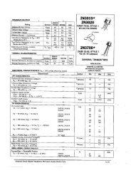
BC807; BC807W; BC327 45 V, 500 mA PNP general ... - Maritex
BC807; BC807W; BC327 45 V, 500 mA PNP general ... - Maritex
BC807; BC807W; BC327 45 V, 500 mA PNP general ... - Maritex
- TAGS
- BC807

Create successful ePaper yourself
Turn your PDF publications into a flip-book with our unique Google optimized e-Paper software.
1. Product profile<br />
1.1 General description<br />
<strong>PNP</strong> <strong>general</strong>-purpose transistors.<br />
[1] Also available in SOT54A and SOT54 variant packages (see Section 2).<br />
1.2 Features<br />
<strong>BC807</strong>; <strong>BC807</strong>W; <strong>BC327</strong><br />
<strong>45</strong> V, <strong>500</strong> <strong>mA</strong> <strong>PNP</strong> <strong>general</strong>-purpose transistors<br />
Rev. 05 — 21 February 2005 Product data sheet<br />
Table 1: Product overview<br />
Type number Package NPN complement<br />
Philips JEITA<br />
<strong>BC807</strong> SOT23 - BC817<br />
<strong>BC807</strong>W SOT323 SC-70 BC817W<br />
<strong>BC327</strong> [1] SOT54 (TO-92) SC-43A BC337<br />
■ High current<br />
■ Low voltage<br />
1.3 Applications<br />
■ General-purpose switching and amplification<br />
1.4 Quick reference data<br />
Table 2: Quick reference data<br />
Symbol Parameter Conditions Min Typ Max Unit<br />
VCEO collector-emitter voltage open base;<br />
IC =10<strong>mA</strong><br />
- - −<strong>45</strong> V<br />
IC collector current (DC) - - −<strong>500</strong> <strong>mA</strong><br />
ICM peak collector current - - −1 A<br />
hFE DC current gain IC = −100 <strong>mA</strong>;<br />
VCE = −1 V<br />
[1]<br />
<strong>BC807</strong>; <strong>BC807</strong>W; <strong>BC327</strong> 100 - 600<br />
<strong>BC807</strong>-16; <strong>BC807</strong>-16W; <strong>BC327</strong>-16 100 - 250<br />
<strong>BC807</strong>-25; <strong>BC807</strong>-25W; <strong>BC327</strong>-25 160 - 400<br />
<strong>BC807</strong>-40; <strong>BC807</strong>-40W; <strong>BC327</strong>-40 250 - 600<br />
[1] Pulse test: tp ≤ 300 μs; δ≤ 0.02.
Philips Semiconductors <strong>BC807</strong>; <strong>BC807</strong>W; <strong>BC327</strong><br />
2. Pinning information<br />
Table 3: Pinning<br />
<strong>45</strong> V, <strong>500</strong> <strong>mA</strong> <strong>PNP</strong> <strong>general</strong>-purpose transistors<br />
Pin<br />
SOT23<br />
Description Simplified outline Symbol<br />
1 base<br />
2 emitter<br />
3<br />
3 collector<br />
1<br />
1 2<br />
SOT323<br />
1 base<br />
2 emitter<br />
3 collector<br />
SOT54<br />
1 emitter<br />
2 base<br />
3 collector<br />
SOT54A<br />
1 emitter<br />
2 base<br />
3 collector<br />
SOT54 variant<br />
1 emitter<br />
2 base<br />
3 collector<br />
9397 750 14023 © Koninklijke Philips Electronics N.V. 2005. All rights reserved.<br />
Product data sheet Rev. 05 — 21 February 2005 2 of 19<br />
3<br />
1 2<br />
sot323_so<br />
1<br />
2<br />
3<br />
001aab347<br />
1<br />
2<br />
3<br />
001aab348<br />
1<br />
2<br />
3<br />
001aab447<br />
1<br />
2<br />
3<br />
2<br />
sym013<br />
3<br />
2<br />
sym013<br />
3<br />
1<br />
006aaa149<br />
2<br />
3<br />
1<br />
006aaa149<br />
2<br />
3<br />
1<br />
006aaa149
Philips Semiconductors <strong>BC807</strong>; <strong>BC807</strong>W; <strong>BC327</strong><br />
3. Ordering information<br />
4. Marking<br />
<strong>45</strong> V, <strong>500</strong> <strong>mA</strong> <strong>PNP</strong> <strong>general</strong>-purpose transistors<br />
Table 4: Ordering information<br />
Type number [1] Package<br />
Name Description Version<br />
<strong>BC807</strong> - plastic surface mounted package; 3 leads SOT23<br />
<strong>BC807</strong>W SC-70 plastic surface mounted package; 3 leads SOT323<br />
<strong>BC327</strong> [2] SC-43A plastic single-ended leaded (through hole) package;<br />
3 leads<br />
SOT54<br />
[1] Valid for all available selection groups.<br />
[2] Also available in SOT54A and SOT54 variant packages (see Section 2 and Section 9).<br />
Table 5: Marking codes<br />
Type number Marking code [1]<br />
<strong>BC807</strong> 5D*<br />
<strong>BC807</strong>-16 5A*<br />
<strong>BC807</strong>-25 5B*<br />
<strong>BC807</strong>-40 5C*<br />
<strong>BC807</strong>W 5D*<br />
<strong>BC807</strong>-16W 5A*<br />
<strong>BC807</strong>-25W 5B*<br />
<strong>BC807</strong>-40W 5C*<br />
<strong>BC327</strong> C327<br />
<strong>BC327</strong>-16 C32716<br />
<strong>BC327</strong>-25 C32725<br />
<strong>BC327</strong>-40 C32740<br />
[1] * = -: made in Hong Kong<br />
* = p: made in Hong Kong<br />
* = t: made in Malaysia<br />
* = W: made in China<br />
9397 750 14023 © Koninklijke Philips Electronics N.V. 2005. All rights reserved.<br />
Product data sheet Rev. 05 — 21 February 2005 3 of 19
Philips Semiconductors <strong>BC807</strong>; <strong>BC807</strong>W; <strong>BC327</strong><br />
5. Limiting values<br />
6. Thermal characteristics<br />
<strong>45</strong> V, <strong>500</strong> <strong>mA</strong> <strong>PNP</strong> <strong>general</strong>-purpose transistors<br />
Table 6: Limiting values<br />
In accordance with the Absolute Maximum Rating System (IEC 60134).<br />
Symbol Parameter Conditions Min Max Unit<br />
VCBO collector-base voltage open emitter - −50 V<br />
VCEO collector-emitter voltage open base;<br />
IC =10<strong>mA</strong><br />
- −<strong>45</strong> V<br />
VEBO emitter-base voltage open collector - −5 V<br />
IC collector current (DC) - −<strong>500</strong> <strong>mA</strong><br />
ICM peak collector current - −1 A<br />
IBM peak base current - −200 <strong>mA</strong><br />
Ptot total power dissipation<br />
<strong>BC807</strong> Tamb ≤ 25 °C [1] [2] - 250 mW<br />
<strong>BC807</strong>W Tamb ≤ 25 °C [1] [2] - 200 mW<br />
<strong>BC327</strong> Tamb ≤ 25 °C [1] [2] - 625 mW<br />
Tstg storage temperature −65 +150 °C<br />
Tj junction temperature - 150 °C<br />
Tamb ambient temperature −65 +150 °C<br />
[1] Transistor mounted on an FR4 printed-circuit board, single-sided copper, tin-plated and standard footprint.<br />
[2] Valid for all available selection groups.<br />
Table 7: Thermal characteristics<br />
Symbol Parameter Conditions Min Typ Max Unit<br />
Rth(j-a) thermal resistance from<br />
junction to ambient<br />
<strong>BC807</strong> Tamb ≤ 25 °C [1] [2] - - <strong>500</strong> K/W<br />
<strong>BC807</strong>W Tamb ≤ 25 °C [1] [2] - - 625 K/W<br />
<strong>BC327</strong> Tamb ≤ 25 °C [1] [2] - - 200 K/W<br />
[1] Transistor mounted on an FR4 printed-circuit board, single-sided copper, tin-plated and standard footprint.<br />
[2] Valid for all available selection groups.<br />
9397 750 14023 © Koninklijke Philips Electronics N.V. 2005. All rights reserved.<br />
Product data sheet Rev. 05 — 21 February 2005 4 of 19
Philips Semiconductors <strong>BC807</strong>; <strong>BC807</strong>W; <strong>BC327</strong><br />
7. Characteristics<br />
[1] Pulse test: tp ≤ 300 μs; δ≤ 0.02.<br />
[2] VBE decreases by approximately 2 mV/K with increasing temperature.<br />
<strong>45</strong> V, <strong>500</strong> <strong>mA</strong> <strong>PNP</strong> <strong>general</strong>-purpose transistors<br />
Table 8: Characteristics<br />
Tamb = 25 °C unless otherwise specified.<br />
Symbol Parameter Conditions Min Typ Max Unit<br />
ICBO collector-base cut-off current IE = 0 A; VCB = −20 V - - −100 nA<br />
IE = 0 A; VCB = −20 V;<br />
Tj = 150 °C<br />
- - −5 μA<br />
IEBO emitter-base cut-off current IC = 0 A; VEB = −5 V - - −100 nA<br />
hFE DC current gain IC = −100 <strong>mA</strong>; VCE = −1 V [1]<br />
<strong>BC807</strong>; <strong>BC807</strong>W; <strong>BC327</strong> 100 - 600<br />
<strong>BC807</strong>-16; <strong>BC807</strong>-16W;<br />
<strong>BC327</strong>-16<br />
100 - 250<br />
<strong>BC807</strong>-25; <strong>BC807</strong>-25W;<br />
<strong>BC327</strong>-25<br />
160 - 400<br />
<strong>BC807</strong>-40; <strong>BC807</strong>-40W;<br />
<strong>BC327</strong>-40<br />
250 - 600<br />
hFE DC current gain IC = −<strong>500</strong> <strong>mA</strong>; VCE = −1 V [1] 40 - -<br />
VCEsat collector-emitter saturation<br />
voltage<br />
IC = −<strong>500</strong> <strong>mA</strong>; IB = −50 <strong>mA</strong> [1] - - −700 mV<br />
VBE base-emitter voltage IC = −<strong>500</strong> <strong>mA</strong>; VCE = −1 V [2] - - −1.2 V<br />
Cc collector capacitance IE = ie = 0 A; VCB = −10 V;<br />
f=1MHz<br />
- 5 - pF<br />
fT transition frequency IC = −10 <strong>mA</strong>; VCE = −5 V;<br />
f = 100 MHz<br />
80 - - MHz<br />
9397 750 14023 © Koninklijke Philips Electronics N.V. 2005. All rights reserved.<br />
Product data sheet Rev. 05 — 21 February 2005 5 of 19
Philips Semiconductors <strong>BC807</strong>; <strong>BC807</strong>W; <strong>BC327</strong><br />
hFE<br />
300<br />
200<br />
100<br />
(1)<br />
(2)<br />
(3)<br />
(1)<br />
VCE = −1 V.<br />
Tamb = 150 °C.<br />
(2) Tamb = 25 °C.<br />
(3) Tamb = −55 °C.<br />
Fig 1. Selection -16: DC current gain as a function of<br />
collector current; typical values.<br />
(1)<br />
VCE = −1 V.<br />
Tamb = 150 °C.<br />
(2) Tamb = 25 °C.<br />
(3) Tamb = −55 °C.<br />
006aaa119<br />
0<br />
−10<br />
IC (<strong>mA</strong>)<br />
−1 −103 −102 −1 −10<br />
hFE<br />
800<br />
600<br />
400<br />
200<br />
<strong>45</strong> V, <strong>500</strong> <strong>mA</strong> <strong>PNP</strong> <strong>general</strong>-purpose transistors<br />
(1)<br />
VCE = −1 V.<br />
Tamb = 150 °C.<br />
(2) Tamb = 25 °C.<br />
(3) Tamb = −55 °C.<br />
Fig 2. Selection -25: DC current gain as a function of<br />
collector current; typical values.<br />
Fig 3. Selection -40: DC current gain as a function of collector current; typical values.<br />
(1)<br />
(2)<br />
(3)<br />
006aaa120<br />
9397 750 14023 © Koninklijke Philips Electronics N.V. 2005. All rights reserved.<br />
Product data sheet Rev. 05 — 21 February 2005 6 of 19<br />
hFE<br />
600<br />
400<br />
200<br />
(1)<br />
(2)<br />
(3)<br />
0<br />
−10<br />
IC (<strong>mA</strong>)<br />
−1 −103 −102 −1 −10<br />
006aaa121<br />
0<br />
−10<br />
IC (<strong>mA</strong>)<br />
−1 −103 −102 −1 −10
Philips Semiconductors <strong>BC807</strong>; <strong>BC807</strong>W; <strong>BC327</strong><br />
−10<br />
VBEsat<br />
(V)<br />
−1<br />
(1)<br />
(2)<br />
(3)<br />
(1)<br />
IC/IB = 10.<br />
Tamb = −55 °C.<br />
(2) Tamb = 25 °C.<br />
(3) Tamb = 150 °C.<br />
Fig 4. Selection -16: Base-emitter saturation voltage<br />
as a function of collector current; typical<br />
values.<br />
(1)<br />
IC/IB = 10.<br />
Tamb = −55 °C.<br />
(2) Tamb = 25 °C.<br />
(3) Tamb = 150 °C.<br />
006aaa122<br />
−10<br />
IC (<strong>mA</strong>)<br />
−1 −103 −102 −10<br />
−1 −10<br />
−1<br />
−10<br />
VBEsat<br />
(V)<br />
−1<br />
(1)<br />
(2)<br />
(3)<br />
<strong>45</strong> V, <strong>500</strong> <strong>mA</strong> <strong>PNP</strong> <strong>general</strong>-purpose transistors<br />
(1)<br />
IC/IB = 10.<br />
Tamb = −55 °C.<br />
(2) Tamb = 25 °C.<br />
(3) Tamb = 150 °C.<br />
Fig 5. Selection -25: Base-emitter saturation voltage<br />
as a function of collector current; typical<br />
values.<br />
Fig 6. Selection -40: Base-emitter saturation voltage as a function of collector current; typical values.<br />
006aaa123<br />
−10<br />
IC (<strong>mA</strong>)<br />
−1 −103 −102 −10<br />
−1 −10<br />
−1<br />
9397 750 14023 © Koninklijke Philips Electronics N.V. 2005. All rights reserved.<br />
Product data sheet Rev. 05 — 21 February 2005 7 of 19<br />
−10<br />
VBEsat<br />
(V)<br />
−1<br />
006aaa124<br />
−10<br />
IC (<strong>mA</strong>)<br />
−1 −103 −102 −10<br />
−1 −10<br />
−1<br />
(1)<br />
(2)<br />
(3)
Philips Semiconductors <strong>BC807</strong>; <strong>BC807</strong>W; <strong>BC327</strong><br />
−1<br />
VCEsat<br />
(V)<br />
−10 −1<br />
(1)<br />
IC/IB = 10.<br />
Tamb = 150 °C.<br />
(2) Tamb = 25 °C.<br />
(3) Tamb = −55 °C.<br />
Fig 7. Selection -16: Collector-emitter saturation<br />
voltage as a function of collector current;<br />
typical values.<br />
(1)<br />
IC/IB = 10.<br />
Tamb = 150 °C.<br />
(2) Tamb = 25 °C.<br />
(3) Tamb = −55 °C.<br />
006aaa125<br />
−10<br />
IC (<strong>mA</strong>)<br />
−1 −103 −102 −10<br />
−1 −10<br />
−2<br />
(1)<br />
(3)<br />
(2)<br />
−1<br />
VCEsat<br />
(V)<br />
−10 −1<br />
−10 −2<br />
<strong>45</strong> V, <strong>500</strong> <strong>mA</strong> <strong>PNP</strong> <strong>general</strong>-purpose transistors<br />
(1)<br />
IC/IB = 10.<br />
Tamb = 150 °C.<br />
(2) Tamb = 25 °C.<br />
(3) Tamb = −55 °C.<br />
006aaa126<br />
Fig 8. Selection- 25: Collector-emitter saturation<br />
voltage as a function of collector current;<br />
typical values.<br />
Fig 9. Selection -40: Collector-emitter saturation voltage as a function of collector current; typical values.<br />
9397 750 14023 © Koninklijke Philips Electronics N.V. 2005. All rights reserved.<br />
Product data sheet Rev. 05 — 21 February 2005 8 of 19<br />
−1<br />
VCEsat<br />
(V)<br />
−10 −1<br />
−10 −2<br />
−10−3 −10<br />
IC (<strong>mA</strong>)<br />
−1 −103 −102 −1 −10<br />
006aaa127<br />
−10−3 −10<br />
IC (<strong>mA</strong>)<br />
−1 −103 −102 −1 −10<br />
(1)<br />
(2)<br />
(3)<br />
(1)<br />
(3)<br />
(2)
Philips Semiconductors <strong>BC807</strong>; <strong>BC807</strong>W; <strong>BC327</strong><br />
−1.2<br />
IC<br />
(A)<br />
−0.8<br />
−0.4<br />
0<br />
0 −1 −2 −3 −4 −5<br />
VCE (V)<br />
(1)<br />
Tamb = 25 °C.<br />
IB = −16.0 <strong>mA</strong>.<br />
(2) IB = −14.4 <strong>mA</strong>.<br />
(3) IB = −12.8 <strong>mA</strong>.<br />
(4) IB = −11.2 <strong>mA</strong>.<br />
(5) IB = −9.6 <strong>mA</strong>.<br />
(6) IB = −8.0 <strong>mA</strong>.<br />
(7) IB = −6.4 <strong>mA</strong>.<br />
(8) IB = −4.8 <strong>mA</strong>.<br />
(9) IB = −3.2 <strong>mA</strong>.<br />
(10) IB = −1.6 <strong>mA</strong>.<br />
(3) (2)<br />
006aaa128<br />
Fig 10. Selection -16: Collector current as a function of<br />
collector-emitter voltage; typical values.<br />
(1)<br />
(4)<br />
(5)<br />
(6)<br />
(7)<br />
(8)<br />
(9)<br />
(10)<br />
<strong>45</strong> V, <strong>500</strong> <strong>mA</strong> <strong>PNP</strong> <strong>general</strong>-purpose transistors<br />
0<br />
0 −1 −2 −3 −4 −5<br />
VCE (V)<br />
(1)<br />
Tamb = 25 °C.<br />
IB = −13.0 <strong>mA</strong>.<br />
(2) IB = −11.7 <strong>mA</strong>.<br />
(3) IB = −10.4 <strong>mA</strong>.<br />
(4) IB = −9.1 <strong>mA</strong>.<br />
(5) IB = −7.8 <strong>mA</strong>.<br />
(6) IB = −6.5 <strong>mA</strong>.<br />
(7) IB = −5.2 <strong>mA</strong>.<br />
(8) IB = −3.9 <strong>mA</strong>.<br />
(9) IB = −2.6 <strong>mA</strong>.<br />
(10) IB = −1.3 <strong>mA</strong>.<br />
006aaa129<br />
Fig 11. Selection -25: Collector current as a function of<br />
collector-emitter voltage; typical values.<br />
9397 750 14023 © Koninklijke Philips Electronics N.V. 2005. All rights reserved.<br />
Product data sheet Rev. 05 — 21 February 2005 9 of 19<br />
−1.2<br />
IC<br />
(A)<br />
−0.8<br />
−0.4<br />
(3)<br />
(2)<br />
(1)<br />
(4)<br />
(5)<br />
(6)<br />
(7)<br />
(8)<br />
(9)<br />
(10)
Philips Semiconductors <strong>BC807</strong>; <strong>BC807</strong>W; <strong>BC327</strong><br />
(1)<br />
Tamb = 25 °C.<br />
IB = −12.0 <strong>mA</strong>.<br />
(2) IB = −10.8 <strong>mA</strong>.<br />
(3) IB = −9.6 <strong>mA</strong>.<br />
(4) IB = −8.4 <strong>mA</strong>.<br />
(5) IB = −7.2 <strong>mA</strong>.<br />
(6) IB = −6.0 <strong>mA</strong>.<br />
(7) IB = −4.8 <strong>mA</strong>.<br />
(8) IB = −3.6 <strong>mA</strong>.<br />
(9) IB = −2.4 <strong>mA</strong>.<br />
(10) IB = −1.2 <strong>mA</strong>.<br />
−1.2<br />
IC<br />
(A)<br />
−0.8<br />
−0.4<br />
0<br />
0 −1 −2 −3 −4 −5<br />
VCE (V)<br />
<strong>45</strong> V, <strong>500</strong> <strong>mA</strong> <strong>PNP</strong> <strong>general</strong>-purpose transistors<br />
006aaa130<br />
Fig 12. Selection -40: Collector current as a function of collector-emitter voltage; typical values.<br />
9397 750 14023 © Koninklijke Philips Electronics N.V. 2005. All rights reserved.<br />
Product data sheet Rev. 05 — 21 February 2005 10 of 19<br />
(5)<br />
(4)<br />
(3)<br />
(2)<br />
(1)<br />
(6)<br />
(7)<br />
(8)<br />
(9)<br />
(10)
Philips Semiconductors <strong>BC807</strong>; <strong>BC807</strong>W; <strong>BC327</strong><br />
8. Package outline<br />
UNIT<br />
OUTLINE<br />
VERSION<br />
A 1<br />
max.<br />
Fig 13. Package outline SOT23 (TO-236AB).<br />
bp c D E e e1 HE Lp Q v w<br />
REFERENCES<br />
<strong>45</strong> V, <strong>500</strong> <strong>mA</strong> <strong>PNP</strong> <strong>general</strong>-purpose transistors<br />
Plastic surface mounted package; 3 leads SOT23<br />
DIMENSIONS (mm are the original dimensions)<br />
A<br />
1.1<br />
mm 0.1<br />
0.9<br />
0.48<br />
0.38<br />
0.15<br />
0.09<br />
3.0<br />
2.8<br />
1.4<br />
1.2<br />
1.9<br />
0.95<br />
IEC JEDEC JEITA<br />
SOT23 TO-236AB<br />
D<br />
1 2<br />
e1<br />
e<br />
3<br />
bp<br />
B<br />
w M B<br />
EUROPEAN<br />
PROJECTION<br />
ISSUE DATE<br />
99-09-13<br />
04-11-04<br />
9397 750 14023 © Koninklijke Philips Electronics N.V. 2005. All rights reserved.<br />
Product data sheet Rev. 05 — 21 February 2005 11 of 19<br />
2.5<br />
2.1<br />
A<br />
0.<strong>45</strong><br />
0.15<br />
A1<br />
0 1 2 mm<br />
scale<br />
0.55<br />
0.<strong>45</strong><br />
E<br />
H E<br />
0.2<br />
detail X<br />
0.1<br />
A<br />
Lp<br />
Q<br />
c<br />
X<br />
v M A
Philips Semiconductors <strong>BC807</strong>; <strong>BC807</strong>W; <strong>BC327</strong><br />
UNIT<br />
A 1<br />
max<br />
Fig 14. Package outline SOT323 (SC-70).<br />
bp c D E e e1 HE Lp Q v w<br />
<strong>45</strong> V, <strong>500</strong> <strong>mA</strong> <strong>PNP</strong> <strong>general</strong>-purpose transistors<br />
Plastic surface mounted package; 3 leads SOT323<br />
DIMENSIONS (mm are the original dimensions)<br />
A<br />
1.1<br />
mm 0.1<br />
0.8<br />
OUTLINE<br />
VERSION<br />
y<br />
0.4<br />
0.3<br />
0.25<br />
0.10<br />
D<br />
1 2<br />
e1<br />
e<br />
2.2<br />
1.8<br />
1.35<br />
1.15<br />
1.3<br />
0.65<br />
REFERENCES<br />
IEC JEDEC JEITA<br />
SOT323 SC-70<br />
3<br />
bp<br />
B<br />
w M<br />
B<br />
EUROPEAN<br />
PROJECTION<br />
ISSUE DATE<br />
9397 750 14023 © Koninklijke Philips Electronics N.V. 2005. All rights reserved.<br />
Product data sheet Rev. 05 — 21 February 2005 12 of 19<br />
2.2<br />
2.0<br />
A<br />
A1<br />
0 1 2 mm<br />
scale<br />
0.<strong>45</strong><br />
0.15<br />
0.23<br />
0.13<br />
E<br />
H E<br />
0.2<br />
detail X<br />
Lp<br />
0.2<br />
A<br />
Q<br />
c<br />
X<br />
v M A<br />
97-02-28<br />
04-11-04
Philips Semiconductors <strong>BC807</strong>; <strong>BC807</strong>W; <strong>BC327</strong><br />
UNIT A<br />
OUTLINE<br />
VERSION<br />
Fig 15. Package outline SOT54 (SC-43A/TO-92).<br />
REFERENCES<br />
<strong>45</strong> V, <strong>500</strong> <strong>mA</strong> <strong>PNP</strong> <strong>general</strong>-purpose transistors<br />
Plastic single-ended leaded (through hole) package; 3 leads SOT54<br />
mm<br />
D<br />
5.2<br />
5.0<br />
d<br />
DIMENSIONS (mm are the original dimensions)<br />
b<br />
0.48<br />
0.40<br />
E<br />
1<br />
2<br />
3<br />
b1 0.66<br />
0.55<br />
b 1<br />
c<br />
0.<strong>45</strong><br />
0.38<br />
D<br />
4.8<br />
4.4<br />
d<br />
1.7<br />
1.4<br />
IEC JEDEC JEITA<br />
E<br />
4.2<br />
3.6<br />
e<br />
2.54<br />
EUROPEAN<br />
PROJECTION<br />
ISSUE DATE<br />
9397 750 14023 © Koninklijke Philips Electronics N.V. 2005. All rights reserved.<br />
Product data sheet Rev. 05 — 21 February 2005 13 of 19<br />
e 1<br />
1.27<br />
L<br />
14.5<br />
12.7<br />
L 1 (1)<br />
max.<br />
Note<br />
1. Terminal dimensions within this zone are uncontrolled to allow for flow of plastic and terminal irregularities.<br />
SOT54 TO-92 SC-43A<br />
A L<br />
0 2.5 5 mm<br />
scale<br />
L 1<br />
2.5<br />
b<br />
c<br />
e 1<br />
e<br />
04-06-28<br />
04-11-16
Philips Semiconductors <strong>BC807</strong>; <strong>BC807</strong>W; <strong>BC327</strong><br />
UNIT A<br />
OUTLINE<br />
VERSION<br />
Fig 16. Package outline SOT54A.<br />
REFERENCES<br />
<strong>45</strong> V, <strong>500</strong> <strong>mA</strong> <strong>PNP</strong> <strong>general</strong>-purpose transistors<br />
Plastic single-ended leaded (through hole) package; 3 leads (wide pitch) SOT54A<br />
mm<br />
D<br />
DIMENSIONS (mm are the original dimensions)<br />
5.2<br />
5.0<br />
b<br />
0.48<br />
0.40<br />
b1 0.66<br />
0.55<br />
c<br />
0.<strong>45</strong><br />
0.38<br />
D<br />
4.8<br />
4.4<br />
d<br />
1.7<br />
1.4<br />
IEC JEDEC JEITA<br />
E<br />
4.2<br />
3.6<br />
e<br />
5.08<br />
EUROPEAN<br />
PROJECTION<br />
ISSUE DATE<br />
9397 750 14023 © Koninklijke Philips Electronics N.V. 2005. All rights reserved.<br />
Product data sheet Rev. 05 — 21 February 2005 14 of 19<br />
e 1<br />
2.54<br />
L<br />
14.5<br />
12.7<br />
L 1 (1)<br />
max.<br />
Note<br />
1. Terminal dimensions within this zone are uncontrolled to allow for flow of plastic and terminal irregularities.<br />
SOT54A<br />
d<br />
E<br />
1<br />
2<br />
3<br />
b1<br />
A L<br />
0 2.5 5 mm<br />
scale<br />
L 2<br />
L 1<br />
3<br />
L 2<br />
3<br />
2<br />
b<br />
c<br />
e 1<br />
e<br />
97-05-13<br />
04-06-28
Philips Semiconductors <strong>BC807</strong>; <strong>BC807</strong>W; <strong>BC327</strong><br />
UNIT A<br />
OUTLINE<br />
VERSION<br />
Fig 17. Package outline SOT54 variant.<br />
REFERENCES<br />
<strong>45</strong> V, <strong>500</strong> <strong>mA</strong> <strong>PNP</strong> <strong>general</strong>-purpose transistors<br />
Plastic single-ended leaded (through hole) package; 3 leads (on-circle) SOT54 variant<br />
mm<br />
D<br />
DIMENSIONS (mm are the original dimensions)<br />
5.2<br />
5.0<br />
b<br />
0.48<br />
0.40<br />
b1 0.66<br />
0.55<br />
c<br />
0.<strong>45</strong><br />
0.38<br />
D<br />
4.8<br />
4.4<br />
d<br />
1.7<br />
1.4<br />
IEC JEDEC JEITA<br />
E<br />
4.2<br />
3.6<br />
e<br />
2.54<br />
EUROPEAN<br />
PROJECTION<br />
ISSUE DATE<br />
9397 750 14023 © Koninklijke Philips Electronics N.V. 2005. All rights reserved.<br />
Product data sheet Rev. 05 — 21 February 2005 15 of 19<br />
e 1<br />
1.27<br />
L<br />
14.5<br />
12.7<br />
L 1 (1)<br />
max<br />
L 2<br />
max<br />
2.5 2.5<br />
Note<br />
1. Terminal dimensions within this zone are uncontrolled to allow for flow of plastic and terminal irregularities.<br />
SOT54 variant<br />
d<br />
E<br />
1<br />
2<br />
3<br />
b 1<br />
A L<br />
0 2.5 5 mm<br />
scale<br />
L 2<br />
L 1<br />
c<br />
b<br />
e 1<br />
e 1<br />
e<br />
04-06-28<br />
05-01-10
Philips Semiconductors <strong>BC807</strong>; <strong>BC807</strong>W; <strong>BC327</strong><br />
9. Packing information<br />
Table 9: Packing methods<br />
The indicated -xxx are the last three digits of the 12NC ordering code. [1]<br />
[1] For further information and the availability of packing methods, see Section 14.<br />
<strong>45</strong> V, <strong>500</strong> <strong>mA</strong> <strong>PNP</strong> <strong>general</strong>-purpose transistors<br />
Type number Package Description Packing quantity<br />
3000 <strong>500</strong>0 10000<br />
<strong>BC807</strong> SOT23 4 mm pitch, 8 mm tape and reel -215 - -235<br />
<strong>BC807</strong>W SOT323 4 mm pitch, 8 mm tape and reel -115 - -135<br />
<strong>BC327</strong> SOT54 bulk, straight leads - -412 -<br />
<strong>BC327</strong> SOT54A tape and reel, wide pitch - - -116<br />
<strong>BC327</strong> SOT54A tape ammopack, wide pitch - - -126<br />
<strong>BC327</strong> SOT 54 variant bulk, delta pinning (on-circle) - -112 -<br />
9397 750 14023 © Koninklijke Philips Electronics N.V. 2005. All rights reserved.<br />
Product data sheet Rev. 05 — 21 February 2005 16 of 19
Philips Semiconductors <strong>BC807</strong>; <strong>BC807</strong>W; <strong>BC327</strong><br />
10. Revision history<br />
Table 10: Revision history<br />
<strong>45</strong> V, <strong>500</strong> <strong>mA</strong> <strong>PNP</strong> <strong>general</strong>-purpose transistors<br />
Document ID Release date Data sheet status Change notice Doc. number Supersedes<br />
<strong>BC807</strong>_<strong>BC807</strong>W_<br />
<strong>BC327</strong>_5<br />
20050221 Product data sheet CPCN200302007F<br />
CPCN20040<strong>500</strong>6F<br />
9397 750 14023 <strong>BC807</strong>_4;<br />
<strong>BC807</strong>W_3;<br />
<strong>BC327</strong>_3<br />
Modifications: • The format of the data sheet has been redesigned to comply with the new presentation and<br />
information standard of Philips Semiconductors.<br />
• This data sheet is a combination of the previous data sheets <strong>BC807</strong>_4, <strong>BC807</strong>W_3 and<br />
<strong>BC327</strong>_3.<br />
• Table 1 and 2 added<br />
• Table 3 Discrete pinning for SOT54A and SOT54 variant added<br />
• Table 5 Marking codes for <strong>BC327</strong>, <strong>BC327</strong>-16, <strong>BC327</strong>-25 and <strong>BC327</strong>-40 added<br />
• Table 8 Typical value for Cc changed to 5 pF according to CPCN200302007F1<br />
• Figure 1, 2 and 3 amended<br />
• Figure 4, 5, 6, 7, 8, 9, 10, 11 and 12 added<br />
• Figure 15 changed according to CPCN20040<strong>500</strong>6F<br />
• Figure 16 and 17 added<br />
• Section 9 added<br />
<strong>BC807</strong>_4 20040116 Product specification - 9397 750 12393 <strong>BC807</strong>_3<br />
<strong>BC807</strong>W_3 19990518 Product specification - 9397 750 05954 <strong>BC807</strong>W_808W_<br />
CNV_2<br />
<strong>BC327</strong>_3 19990415 Product specification - 9397 750 05675 <strong>BC327</strong>_2<br />
9397 750 14023 © Koninklijke Philips Electronics N.V. 2005. All rights reserved.<br />
Product data sheet Rev. 05 — 21 February 2005 17 of 19
Philips Semiconductors <strong>BC807</strong>; <strong>BC807</strong>W; <strong>BC327</strong><br />
11. Data sheet status<br />
<strong>45</strong> V, <strong>500</strong> <strong>mA</strong> <strong>PNP</strong> <strong>general</strong>-purpose transistors<br />
Level Data sheet status [1] Product status [2] [3] Definition<br />
I Objective data Development This data sheet contains data from the objective specification for product development. Philips<br />
Semiconductors reserves the right to change the specification in any manner without notice.<br />
II Preliminary data Qualification This data sheet contains data from the preliminary specification. Supplementary data will be published<br />
at a later date. Philips Semiconductors reserves the right to change the specification without notice, in<br />
order to improve the design and supply the best possible product.<br />
III Product data Production This data sheet contains data from the product specification. Philips Semiconductors reserves the<br />
right to make changes at any time in order to improve the design, manufacturing and supply. Relevant<br />
changes will be communicated via a Customer Product/Process Change Notification (CPCN).<br />
[1] Please consult the most recently issued data sheet before initiating or completing a design.<br />
[2] The product status of the device(s) described in this data sheet may have changed since this data sheet was published. The latest information is available on the Internet at<br />
URL http://www.semiconductors.philips.com.<br />
[3] For data sheets describing multiple type numbers, the highest-level product status determines the data sheet status.<br />
12. Definitions<br />
Short-form specification — The data in a short-form specification is<br />
extracted from a full data sheet with the same type number and title. For<br />
detailed information see the relevant data sheet or data handbook.<br />
Limiting values definition — Limiting values given are in accordance with<br />
the Absolute Maximum Rating System (IEC 60134). Stress above one or<br />
more of the limiting values may cause permanent damage to the device.<br />
These are stress ratings only and operation of the device at these or at any<br />
other conditions above those given in the Characteristics sections of the<br />
specification is not implied. Exposure to limiting values for extended periods<br />
may affect device reliability.<br />
Application information — Applications that are described herein for any<br />
of these products are for illustrative purposes only. Philips Semiconductors<br />
make no representation or warranty that such applications will be suitable for<br />
the specified use without further testing or modification.<br />
14. Contact information<br />
13. Disclaimers<br />
Life support — These products are not designed for use in life support<br />
appliances, devices, or systems where malfunction of these products can<br />
reasonably be expected to result in personal injury. Philips Semiconductors<br />
customers using or selling these products for use in such applications do so<br />
at their own risk and agree to fully indemnify Philips Semiconductors for any<br />
damages resulting from such application.<br />
Right to make changes — Philips Semiconductors reserves the right to<br />
make changes in the products - including circuits, standard cells, and/or<br />
software - described or contained herein in order to improve design and/or<br />
performance. When the product is in full production (status ‘Production’),<br />
relevant changes will be communicated via a Customer Product/Process<br />
Change Notification (CPCN). Philips Semiconductors assumes no<br />
responsibility or liability for the use of any of these products, conveys no<br />
license or title under any patent, copyright, or mask work right to these<br />
products, and makes no representations or warranties that these products are<br />
free from patent, copyright, or mask work right infringement, unless otherwise<br />
specified.<br />
For additional information, please visit: http://www.semiconductors.philips.com<br />
For sales office addresses, send an email to: sales.addresses@www.semiconductors.philips.com<br />
9397 750 14023 © Koninklijke Philips Electronics N.V. 2005. All rights reserved.<br />
Product data sheet Rev. 05 — 21 February 2005 18 of 19
Philips Semiconductors <strong>BC807</strong>; <strong>BC807</strong>W; <strong>BC327</strong><br />
15. Contents<br />
1 Product profile . . . . . . . . . . . . . . . . . . . . . . . . . . 1<br />
1.1 General description. . . . . . . . . . . . . . . . . . . . . . 1<br />
1.2 Features . . . . . . . . . . . . . . . . . . . . . . . . . . . . . . 1<br />
1.3 Applications . . . . . . . . . . . . . . . . . . . . . . . . . . . 1<br />
1.4 Quick reference data. . . . . . . . . . . . . . . . . . . . . 1<br />
2 Pinning information . . . . . . . . . . . . . . . . . . . . . . 2<br />
3 Ordering information . . . . . . . . . . . . . . . . . . . . . 3<br />
4 Marking . . . . . . . . . . . . . . . . . . . . . . . . . . . . . . . . 3<br />
5 Limiting values. . . . . . . . . . . . . . . . . . . . . . . . . . 4<br />
6 Thermal characteristics. . . . . . . . . . . . . . . . . . . 4<br />
7 Characteristics. . . . . . . . . . . . . . . . . . . . . . . . . . 5<br />
8 Package outline . . . . . . . . . . . . . . . . . . . . . . . . 11<br />
9 Packing information. . . . . . . . . . . . . . . . . . . . . 16<br />
10 Revision history . . . . . . . . . . . . . . . . . . . . . . . . 17<br />
11 Data sheet status . . . . . . . . . . . . . . . . . . . . . . . 18<br />
12 Definitions . . . . . . . . . . . . . . . . . . . . . . . . . . . . 18<br />
13 Disclaimers. . . . . . . . . . . . . . . . . . . . . . . . . . . . 18<br />
14 Contact information . . . . . . . . . . . . . . . . . . . . 18<br />
<strong>45</strong> V, <strong>500</strong> <strong>mA</strong> <strong>PNP</strong> <strong>general</strong>-purpose transistors<br />
© Koninklijke Philips Electronics N.V. 2005<br />
All rights are reserved. Reproduction in whole or in part is prohibited without the prior<br />
written consent of the copyright owner. The information presented in this document does<br />
not form part of any quotation or contract, is believed to be accurate and reliable and may<br />
be changed without notice. No liability will be accepted by the publisher for any<br />
consequence of its use. Publication thereof does not convey nor imply any license under<br />
patent- or other industrial or intellectual property rights.<br />
Date of release: 21 February 2005<br />
Document number: 9397 750 14023<br />
Published in The Netherlands