TDA7350 - EBG - Darmstadt
TDA7350 - EBG - Darmstadt
TDA7350 - EBG - Darmstadt

Create successful ePaper yourself
Turn your PDF publications into a flip-book with our unique Google optimized e-Paper software.
®<br />
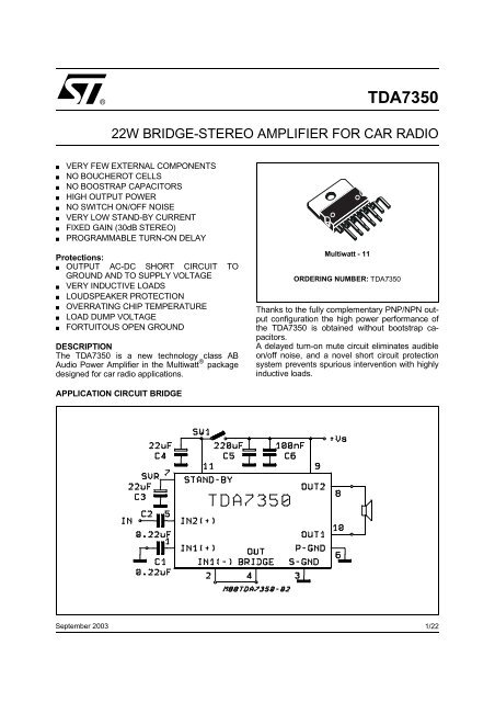
<strong>TDA7350</strong><br />
22W BRIDGE-STEREO AMPLIFIER FOR CAR RADIO<br />
VERY FEW EXTERNAL COMPONENTS<br />
NO BOUCHEROT CELLS<br />
NO BOOSTRAP CAPACITORS<br />
HIGH OUTPUT POWER<br />
NO SWITCH ON/OFF NOISE<br />
VERY LOW STAND-BY CURRENT<br />
FIXED GAIN (30dB STEREO)<br />
PROGRAMMABLE TURN-ON DELAY<br />
Protections:<br />
OUTPUT AC-DC SHORT CIRCUIT TO<br />
GROUND AND TO SUPPLY VOLTAGE<br />
VERY INDUCTIVE LOADS<br />
LOUDSPEAKER PROTECTION<br />
OVERRATING CHIP TEMPERATURE<br />
LOAD DUMP VOLTAGE<br />
FORTUITOUS OPEN GROUND<br />
DESCRIPTION<br />
The <strong>TDA7350</strong> is a new technology class AB<br />
Audio Power Amplifier in the Multiwatt ® package<br />
designed for car radio applications.<br />
APPLICATION CIRCUIT BRIDGE<br />
September 2003<br />
Multiwatt - 11<br />
ORDERING NUMBER: <strong>TDA7350</strong><br />
Thanks to the fully complementary PNP/NPN output<br />
configuration the high power performance of<br />
the <strong>TDA7350</strong> is obtained without bootstrap capacitors.<br />
A delayed turn-on mute circuit eliminates audible<br />
on/off noise, and a novel short circuit protection<br />
system prevents spurious intervention with highly<br />
inductive loads.<br />
This is advanced information on a new product now in development or undergoing evaluation. Details are subject to change without notice.<br />
1/22
<strong>TDA7350</strong><br />
PIN CONNECTION (Top view)<br />
ABSOLUTE MAXIMUM RATINGS<br />
Symbol Parameter Test Conditions Unit<br />
VS Operating Supply Voltage 18 V<br />
VS DC Supply Voltage 28 V<br />
VS Peak Supply Voltage (for t = 50ms) 40 V<br />
Io Output Peak Current (non rep. for t = 100μs) 5 A<br />
Io Output Peak Current (rep. freq. > 10Hz) 4 A<br />
Ptot Power Dissipation at Tcase = 85°C 36 W<br />
Tstg,TJ Storage and Junction Temperature -40 to 150 °C<br />
THERMAL DATA<br />
Symbol Description Value Unit<br />
Rthj-case Thermal Resistance Junction-case Max 1.8 °C/W<br />
2/22
ELECTRICAL CHARACTERISTICS (Refer to the test circuits, Tamb = 25°C, VS = 14.4V, f = 1KHz unless<br />
otherwise specified)<br />
Symbol Parameter Test Condition Min. Typ. Max. Unit<br />
VS Supply Voltage Range 8 18 V<br />
Id Total Quiescent Drain Current stereo configuration 120 mA<br />
ASB Stand-by attenuation 60 80 dB<br />
ISB Stand-by Current 100 μA<br />
Tsd Thermal Shut-down Junction<br />
Temperature<br />
150 °C<br />
STEREO<br />
Po Output Power (each channel) d = 10%<br />
RL = 2Ω<br />
RL = 3.2Ω<br />
RL = 4Ω<br />
d = 10%; VS = 13.2V<br />
RL = 2Ω<br />
RL = 3.2Ω<br />
RL = 4Ω<br />
d Distortion Po = 0.1 to 4W; RL = 3.2Ω 0.5 %<br />
SVR Supply Voltage Rejection RS = 10kΩ C3 = 22μF<br />
f = 100Hz C3 = 100μF<br />
45 50<br />
57<br />
dB<br />
CT Crosstalk f = 1KHz<br />
45 55<br />
dB<br />
f = 10KHz<br />
50<br />
dB<br />
RI Input Resistance 30 50 KΩ<br />
GV Voltage Gain 27 29 31 dB<br />
GV Voltage Gain Match 1 dB<br />
EIN Input Noise Voltage RS = 50Ω (*)<br />
RS = 10KΩ (*)<br />
RS = 50Ω (**)<br />
RS = 10KΩ (**)<br />
1.5<br />
2<br />
2<br />
2.7 7<br />
μV<br />
μV<br />
μV<br />
μV<br />
BRIDGE<br />
Po Output Power d = 10%; RL = 4Ω<br />
d = 10%; RL = 3.2Ω<br />
d = 10%; VS = 13.2V<br />
RL = 4Ω<br />
RL = 3.2Ω<br />
d Distortion Po = 0.1 to 10W; RL = 4Ω 1 %<br />
VOS Output Offset Voltage 250 mV<br />
SVR Supply Voltage Rejection RS = 10KΩ C3 = 22μF<br />
f = 100Hz C3 = 100μF<br />
45 50<br />
57<br />
dB<br />
RI Input Resistance 50 KΩ<br />
GV Voltage Gain 33 35 37 dB<br />
EIN Input Noise Voltage RS = 50Ω (*)<br />
RS = 10KΩ (*)<br />
RS = 50Ω (**)<br />
RS = 10KΩ (**)<br />
2<br />
2.5<br />
2.7<br />
3.2<br />
μV<br />
μV<br />
μV<br />
μV<br />
(*) Curve A<br />
(**) 22Hz to 22KHz<br />
7<br />
16<br />
11<br />
8<br />
6.5<br />
9<br />
6.5<br />
5.5<br />
20<br />
22<br />
17.5<br />
19<br />
<strong>TDA7350</strong><br />
W<br />
W<br />
W<br />
W<br />
W<br />
W<br />
W<br />
W<br />
W<br />
W<br />
3/22
<strong>TDA7350</strong><br />
Figure 1: STEREO Test and Appication Circuit<br />
Figure 2: P.C. Board and Layout (STEREO) of the circuit of fig. 1 (1:1 scale)<br />
4/22
Figure 3: BRIDGE Test and Appication Circuit<br />
Figure 4: P.C. Board and Layout (BRIDGE) of the circuit of fig. 3 (1:1 scale)<br />
<strong>TDA7350</strong><br />
5/22
<strong>TDA7350</strong><br />
RECOMMENDED VALUES OF THE EXTERNAL COMPONENTS (ref to the Stereo Test and Application<br />
Circuit)<br />
Component Recommended<br />
Value<br />
Purpose<br />
C1 0.22μF Input<br />
Decoupling<br />
(CH1)<br />
C2 0.22μF Input<br />
Decoupling<br />
(CH2)<br />
C3 100μF Supply Voltage<br />
Rejection<br />
Filtering<br />
Capacitor<br />
C4 22μF Stand-By<br />
ON/OFF Delay<br />
Larger than the Recomm.<br />
Value<br />
Smaller than the Recomm.<br />
Value<br />
— —<br />
— —<br />
Longer Turn-On Delay Time Worse Supply Voltage Rejection.<br />
Shorter Turn-On Delay Time<br />
Danger of Noise (POP)<br />
Delayed Turn-Off by Stand-By<br />
Switch<br />
Danger of Noise (POP)<br />
C5 220μF (min) Supply By-Pass Danger of Oscillations<br />
C6 100nF (min) Supply By-Pass Danger of Oscillations<br />
C7 2200μF Output - Decrease of Low Frequency Cut Off - Increase of Low Frequency Cut Off<br />
Decoupling<br />
CH2<br />
- Longer Turn On Delay<br />
- Shorter Turn On Delay<br />
Figure 5: Output Power vs. Supply Voltage Figure 6: Output Power vs. Supply Voltage<br />
(Stereo)<br />
(Stereo)<br />
Figure 7: Output Power vs. Supply Voltage<br />
(Stereo)<br />
6/22<br />
Figure 8: Output Power vs. Supply Voltage<br />
(Bridge)
Figure 9: Output Power vs. Supply Voltage<br />
(Bridge)<br />
Figure 10: Drain Current vs Supply Voltage<br />
(Stereo)<br />
<strong>TDA7350</strong><br />
Figure 11: Distortion vs Output Power (Stereo) Figure 12: Distortion vs Output Power (Stereo)<br />
Figure 13: Distortion vs Output Power (Stereo) Figure 14: Distortion vs Output Power (Bridge)<br />
7/22
<strong>TDA7350</strong><br />
Figure 15: SVR vs. Frequency & CSVR (Stereo) Figure 16: SVR vs. Frequency & CSVR; (Stereo)<br />
Figure 17: SVR vs. Frequency & CSVR; (Bridge) Figure 18: SVR vs. Frequency & CSVR; (Bridge)<br />
Figure 19: Crosstalk vs. Frequency (Stereo) Figure 20: Power Dissipation & Efficiency vs.<br />
Output Power (Stereo)<br />
8/22
Figure 21: Power Dissipation & Efficiency vs.<br />
Output Power (Stereo)<br />
Figure 22: Power Dissipation & Efficiency vs.<br />
Output Power (Bridge)<br />
Figure 23: Power Dissipation & Efficiency vs.<br />
Output Power (Bridge)<br />
AMPLIFIER ORGANIZATION<br />
The <strong>TDA7350</strong> has been developed taking care of<br />
the key concepts of the modern power audio amplifier<br />
for car radio such as: space and costs sav-<br />
<strong>TDA7350</strong><br />
ing due to the minimized external count, excellent<br />
electrical performances, flexibility in use, superior<br />
reliability thanks to a built-in array of protections.<br />
As a result the following performances has been<br />
achieved:<br />
NO NEED OF BOOTSTRAP CAPACITORS<br />
EVEN AT THE HIGHEST OUTPUT POWER<br />
LEVELS<br />
ABSOLUTE STABILITY WITHOUT EXTER-<br />
NAL COMPENSATION THANKS TO THE IN-<br />
NOVATIVE OUT STAGE CONFIGURATION,<br />
ALSO ALLOWING INTERNALLY FIXED<br />
CLOSED LOOP LOWER THAN COMPETI-<br />
TORS<br />
LOW GAIN (30dB STEREO FIXED WITHOUT<br />
ANY EXTERNAL COMPONENTS) IN ORDER<br />
TO MINIMIZE THE OUTPUT NOISE AND OP-<br />
TIMIZE SVR<br />
SILENT MUTE/ST-BY FUNCTION FEATUR-<br />
ING ABSENCE OF POP ON/OFF NOISE<br />
HIGH SVR<br />
STEREO/BRIDGE OPERATION WITHOUT<br />
ADDITION OF EXTERNAL COMPONENT<br />
AC/DC SHORT CIRCUIT PROTECTION (TO<br />
GND, TO VS, ACROSS THE LOAD)<br />
LOUDSPEAKER PROTECTION<br />
DUMP PROTECTION<br />
BLOCK DESCRIPTION<br />
Polarization<br />
The device is organized with the gain resistors directly<br />
connected to the signal ground pin i.e. without<br />
gain capacitors (fig. 24).<br />
The non inverting inputs of the amplifiers are connected<br />
to the SVR pin by means of resistor dividers,<br />
equal to the feedback networks. This allows<br />
the outputs to track the SVR pin which is sufficiently<br />
slow to avoid audible turn-on and turn-off<br />
transients.<br />
SVR<br />
The voltage ripple on the outputs is equal to the<br />
one on SVR pin: with appropriate selection of<br />
CSVR, more than 55dB of ripple rejection can be<br />
obtained.<br />
Delayed Turn-on (muting)<br />
The CSVR sets a signal turn-on delay too. A circuit<br />
is included which mutes the device until the voltage<br />
on SVR pin reaches ~2.5V typ. (fig. 25). The<br />
mute function is obtained by duplicating the input<br />
differential pair (fig. 26): it can be switched to the<br />
signal source or to an internal mute input. This<br />
feature is necessary to prevent transients at the<br />
inputs reaching the loudspeaker(s) immediately<br />
after power-on).<br />
9/22
<strong>TDA7350</strong><br />
Fig. 25 represents the detailed turn-on transient<br />
with reference to the stereo configuration.<br />
At the power-on the output decoupling capacitors<br />
are charged through an internal path but the device<br />
itself remains switched off (Phase 1 of the<br />
represented diagram).<br />
When the outputs reach the voltage level of about<br />
1V (this means that there is no presence of short<br />
circuits) the device switches on, the SVR capacitor<br />
starts charging itself and the output tracks exactly<br />
the SVR pin.<br />
During this phase the device is muted until the<br />
SVR reaches the "Play" threshold (~2.5V typ.), after<br />
that the music signal starts being played.<br />
Stereo/Bridge Switching<br />
There is also no need for external components for<br />
Figure 24: Block Diagram; Stereo Configuration<br />
10/22<br />
changing from stereo to bridge configuration (figg.<br />
24-27). A simple short circuit between two pins allows<br />
phase reversal at one output, yet maintaining<br />
the quiescent output voltage.<br />
Stand-by<br />
The device is also equipped with a stand-by function,<br />
so that a low current, and hence low cost<br />
switch, can be used for turn on/off.<br />
Stability<br />
The device is provided with an internal compensation<br />
wich allows to reach low values of closed<br />
loop gain.<br />
In this way better performances on S/N ratio and<br />
SVR can be obtained.
Figure 25: Turn-on Delay Circuit<br />
<strong>TDA7350</strong><br />
11/22
<strong>TDA7350</strong><br />
Figure 26: Mute Function Diagram<br />
Figure 27: Block Diagram; Bridge Configuration<br />
12/22
Figure 28: ICV - PNP Gain vs. IC<br />
Figure 29: ICV - PNP VCE(sat) vs. IC<br />
Figure 30: ICV - PNP cut-off frequency vs. IC<br />
OUTPUT STAGE<br />
Poor current capability and low cutoff frequency<br />
are well known limits of the standard lateral PNP.<br />
Composite PNP-NPN power output stages have<br />
been widely used, regardless their high saturation<br />
drop. This drop can be overcome only at the expense<br />
of external components, namely, the bootstrap<br />
capacitors. The availability of 4A isolated<br />
collector PNP (ICV PNP) adds versatility to the<br />
design. The performance of this component, in<br />
terms of gain, VCEsat and cut-off frequency, is<br />
shown in fig. 28, 29, 30 respectively. It is realized<br />
in a new bipolar technology, characterized by topbottom<br />
isolation techniques, allowing the implementation<br />
of low leakage diodes, too. It guarantees<br />
BVCEO > 20V and BVCBO > 50V both for<br />
NPN and PNP transistors. Basically, the connection<br />
shown in fig. 31 has been chosen. First of all<br />
because its voltage swing is rail-to-rail, limited<br />
only by the VCEsat of the output transistors,<br />
which are in the range of 0.3Ω each. Then, the<br />
gain VOUT/VIN is greater than unity, approximately<br />
1+R2/R1. (VCC/2 is fixed by an auxiliary<br />
amplifier common to both channel). It is possible,<br />
controlling the amount of this local feedback, to<br />
force the loop gain (A . β) to less than unity at frequencies<br />
for which the phase shift is 180°. This<br />
means that the output buffer is intrinsically stable<br />
and not prone to oscillation.<br />
Figure 31: The New Output Stage<br />
<strong>TDA7350</strong><br />
In contrast, with the circuit of fig. 32, the solution<br />
adopted to reduce the gain at high frequencies is<br />
the use of an external RC network.<br />
AMPLIFIER BLOCK DIAGRAM<br />
The block diagram of each voltage amplifier is<br />
shown in fig. 33. Regardless of production<br />
spread, the current in each final stage is kept low,<br />
with enough margin on the minimum, below which<br />
cross-over distortion would appear.<br />
13/22
<strong>TDA7350</strong><br />
Figure 32: A Classical Output Stage<br />
Figure 33: Amplifier Block Diagram<br />
BUILT-IN PROTECTION SYSTEMS<br />
Short Circuit Protection<br />
The maximum current the device can deliver can<br />
be calculated by considering the voltage that may<br />
be present at the terminals of a car radio amplifier<br />
and the minimum load impedance.<br />
Apart from consideration concerning the area of<br />
the power transistors it is not difficult to achieve<br />
peak currents of this magnitude (5A peak).<br />
However, it becomes more complicated if AC and<br />
DC short circuit protection is also required.In particular,with<br />
a protection circuit which limits the<br />
output current following the SOA curve of the output<br />
transistors it is possible that in some conditions<br />
(highly reactive loads, for example) the protection<br />
circuit may intervene during normal<br />
operation. For this reason each amplifier has<br />
been equipped with a protection circuit that intervenes<br />
when the output current exceeds 4A.<br />
Fig 34 shows the protection circuit for an NPN<br />
power transistor (a symmetrical circuit applies to<br />
PNP).The VBE of the power is monitored and<br />
gives out a signal,available through a cascode.<br />
This cascode is used to avoid the intervention of<br />
the short circuit protection when the saturation is<br />
14/22<br />
below a given limit.<br />
The signal sets a flip-flop which forces the amplifier<br />
outputs into a high impedance state.<br />
In case of DC short circuit when the short circuit<br />
is removed the flip-flop is reset and restarts the<br />
circuit (fig. 38). In case of AC short circuit or load<br />
shorted in Bridge configuration, the device is continuously<br />
switched in ON/OFF conditions and the<br />
current is limited.<br />
Figure 34: Circuitry for Short Circuit Detection
Load Dump Voltage Surge<br />
The TDA 7350 has a circuit which enables it to<br />
withstand a voltage pulse train on pin 9, of the<br />
type shown in fig. 36.<br />
If the supply voltage peaks to more than 40V,<br />
then an LC filter must be inserted between the<br />
supply and pin 9, in order to assure that the<br />
pulses at pin 9 will be held within the limits<br />
shown.<br />
A suggested LC network is shown in fig. 35.<br />
With this network, a train of pulses with amplitude<br />
up to 120V and width of 2ms can be applied at<br />
point A. This type of protection is ON when the<br />
supply voltage (pulse or DC) exceeds 18V. For<br />
this reason the maximum operating supply voltage<br />
is 18V.<br />
Figure 35<br />
Figure 36<br />
Polarity Inversion<br />
High current (up to 10A) can be handled by the<br />
device with no damage for a longer period than<br />
the blow-out time of a quick 2A fuse (normally<br />
connected in series with the supply). This features<br />
is added to avoid destruction, if during fitting<br />
to the car, a mistake on the connection of the<br />
supply is made.<br />
Open Ground<br />
When the radio is in the ON condition and the<br />
ground is accidentally opened, a standard audio<br />
amplifier will be damaged. On the <strong>TDA7350</strong> protection<br />
diodes are included to avoid any damage.<br />
DC Voltage<br />
The maximum operating DC voltage for the<br />
<strong>TDA7350</strong> is 18V.<br />
However the device can withstand a DC voltage<br />
up to 28V with no damage. This could occur during<br />
winter if two batteries are series connected to<br />
crank the engine.<br />
Thermal Shut-down<br />
The presence of a thermal limiting circuit offers<br />
the following advantages:<br />
1)an overload on the output (even if it is permanent),<br />
or an excessive ambient temperature<br />
can be easily withstood.<br />
2)the heatsink can have a smaller factor of<br />
safety compared with that of a conventional<br />
circuit. There is no device damage in the case<br />
of excessive junction temperature: all happens<br />
is that Po (and therefore Ptot) and Id are<br />
reduced.<br />
The maximum allowable power dissipation depends<br />
upon the size of the external heatsink (i.e.<br />
its thermal resistance); Fig. 37 shows the dissipable<br />
power as a function of ambient temperature<br />
for different thermal resistance.<br />
Figure 37: Maximum Allowable Power<br />
Dissipation vs. Ambient Temperature<br />
Loudspeaker Protection<br />
The <strong>TDA7350</strong> guarantees safe operations even<br />
for the loudspeaker in case of accidental shortcircuit.<br />
Whenever a single OUT to GND, OUT to VS short<br />
circuit occurs both the outputs are switched OFF<br />
so limiting dangerous DC current flowing through<br />
the loudspeaker.<br />
Figure 38: Restart Circuit<br />
<strong>TDA7350</strong><br />
15/22
<strong>TDA7350</strong><br />
APPLICATION HINTS<br />
This section explains briefly how to get the best<br />
from the <strong>TDA7350</strong> and presents some application<br />
circuits with suggestions for the value of the components.These<br />
values can change depending on<br />
the characteristics that the designer of the car radio<br />
wants to obtain,or other parts of the car radio<br />
that are connected to the audio block.<br />
To optimize the performance of the audio part it is<br />
useful (or indispensable) to analyze also the parts<br />
outside this block that can have an interconnection<br />
with the amplifier.<br />
This method can provide components and system<br />
cost saving.<br />
Reducing Turn On-Off Pop<br />
The <strong>TDA7350</strong> has been designed in a way that<br />
the turn on(off) transients are controlled through<br />
the charge(discharge) of the Csvr capacitor.<br />
As a result of it, the turn on(off) transient spectrum<br />
contents is limited only to the subsonic<br />
range.The following section gives some brief<br />
notes to get the best from this design feature(it<br />
will refer mainly to the stereo application which<br />
appears to be in most cases the more critical from<br />
the pop viewpoint.The bridge connection in<br />
fact,due to the common mode waveform at the<br />
outputs,does not give pop effect).<br />
TURN-ON<br />
Fig 39 shows the output waveform (before and<br />
after the "A" weighting filter) compared to the<br />
value of Csvr.<br />
Better pop-on performance is obtained with<br />
higher Csvr values (the recommended range is<br />
from 22uF to 220uF).<br />
The turn-on delay (during which the amplifier is in<br />
mute condition) is a function essentially of : Cout ,<br />
Csvr .<br />
Being:<br />
T1 ≈ 120 • Cout<br />
T2 ≈ 1200 • Csvr<br />
The turn-on delay is given by:<br />
T1+T2 STEREO<br />
T2 BRIDGE<br />
The best performance is obtained by driving the<br />
st-by pin with a ramp having a slope slower than<br />
2V/ms<br />
16/22<br />
Figure 39:<br />
a) Csvr = 22 μF<br />
b) Csvr = 47 μF<br />
c) Csvr = 100 μF
TURN-OFF<br />
A turn-off pop can occur if the st-by pin goes low<br />
with a short time constant (this can occur if other<br />
car radio sections, preamplifiers,radio.. are supplied<br />
through the same st-by switch).<br />
This pop is due to the fast switch-off of the internal<br />
current generator of the amplifier.<br />
If the voltage present across the load becomes<br />
rapidly zero (due to the fast switch off) a small<br />
pop occurs, depending also on Cout,Rload.<br />
The parameters that set the switch off time constant<br />
of the st-by pin are:<br />
♦ the st-by capacitor (Cst-by)<br />
♦ the SVR capacitor (Csvr)<br />
♦ resistors connected from st-by pin to ground<br />
(Rext)<br />
The time constant is given by :<br />
T ≈ Csvr • 2000Ω // Rext + Cst-by • 2500Ω // Rext<br />
The suggested time constants are :<br />
T > 120ms with Cout=1000μF,RL = 4ohm,stereo<br />
T > 170ms with Cout=2200μF,RL = 4ohm,stereo<br />
If Rext is too low the Csvr can become too high<br />
and a different approach may be useful (see next<br />
section).<br />
Figg 40, 41 show some types of electronic<br />
switches (μP compatible) suitable for supplying<br />
the st-by pin (it is important that Qsw is able to<br />
saturate with VCE ≤ 150mV).<br />
Also for turn off pop the bridge configuration is su-<br />
Figure 40<br />
Figure 41<br />
<strong>TDA7350</strong><br />
perior, in particular the st-by pin can go low faster.<br />
GLOBAL APPROACH TO SOLVING POP<br />
PROBLEM BY USING THE MUTING/TURN ON<br />
DELAY FUNCTION<br />
In the real case turn-on and turn-off pop problems<br />
are generated not only by the power amplifier,but<br />
also (very often) by preamplifiers,tone controls,radios<br />
etc. and transmitted by the power amplifier to<br />
the loudspeaker.<br />
A simple approach to solving these problems is to<br />
use the mute characteristics of the <strong>TDA7350</strong>.<br />
If the SVR pin is at a voltage below 1.5 V, the<br />
mute attenuation (typ)is 30dB .The amplifier is in<br />
play mode when Vsvr overcomes 3.5 V.<br />
With the circuit of fig 42 we can mute the amplifier<br />
for a time Ton after switch-on and for a time Toff<br />
after switch-off.During this period the circuitry that<br />
precedes the power amplifier can produce spurious<br />
spikes that are not transmitted to the loudspeaker.<br />
This can give back a very simple design<br />
of this circuitry from the pop point of view.<br />
A timing diagram of this circuit is illustrated in fig<br />
43. Other advantages of this circuit are:<br />
- A reduced time constant allowance of stand-by<br />
pin turn off.Consequently it is possible to drive all<br />
the car-radio with the signal that drives this pin.<br />
-A better turn-off noise with signal on the output.<br />
To drive two stereo amplifiers with this circuit it is<br />
possible to use the circuit of fig 44.<br />
17/22
<strong>TDA7350</strong><br />
Figure 42<br />
Figure 43<br />
18/22
Figure 44<br />
BALANCE INPUT IN BRIDGE CONFIGURATION<br />
A helpful characteristic of the <strong>TDA7350</strong> is that,in<br />
bridge configuration, a signal present on both the<br />
input capacitors is amplified by the same amount<br />
Figure 45<br />
Figure 46<br />
<strong>TDA7350</strong><br />
and it is present in phase at the outputs,so this<br />
signal does not produce effects on the load.The<br />
typical value of CMRR is 46 dB.<br />
Looking at fig 45, we can see that a noise signal<br />
from the ground of the power amplifier to the<br />
ground of the hypothetical preamplifier is amplified<br />
of a factor equal to the gain of the amplifier<br />
(2 • Gv).<br />
Using a configuration of fig. 46 the same ground<br />
noise is present at the output multiplied by the<br />
factor 2 • Gv/200.<br />
This means less distortion,less noise (e.g. motor<br />
cassette noise ) and/or a simplification of the layout<br />
of PC board.<br />
The only limitation of this balanced input is the<br />
maximum amplitude of common mode signals<br />
(few tens of millivolt) to avoid a loss of output<br />
power due to the common mode signal on the<br />
output, but in a large number of cases this signal<br />
is within this range.<br />
HIGH GAIN ,LOW NOISE APPLICATION<br />
The following section describes a flexible preamplifier<br />
having the purpose to increase the gain of<br />
the <strong>TDA7350</strong>.<br />
19/22
<strong>TDA7350</strong><br />
A two transistor network (fig. 47) has been<br />
adopted whose components can be changed in<br />
order to achieve the desired gain without affecting<br />
the good performances of the audio amplifier itself.<br />
The recommended values for 40 dB overall gain<br />
are :<br />
Figure 47<br />
20/22<br />
Resistance Stereo Bridge<br />
R1<br />
R2<br />
R3<br />
R4<br />
10KΩ<br />
4.3KΩ<br />
10KΩ<br />
50KΩ<br />
10KW<br />
16KΩ<br />
24KΩ<br />
50KΩ
DIM.<br />
MIN.<br />
mm<br />
TYP. MAX. MIN.<br />
inch<br />
TYP. MAX.<br />
A 5 0.197<br />
B 2.65 0.104<br />
C 1.6 0.063<br />
D 1 0.039<br />
E 0.49 0.55 0.019 0.022<br />
F 0.88 0.95 0.035 0.037<br />
G 1.45 1.7 1.95 0.057 0.067 0.077<br />
G1 16.75 17 17.25 0.659 0.669 0.679<br />
H1 19.6 0.772<br />
H2 20.2 0.795<br />
L 21.9 22.2 22.5 0.862 0.874 0.886<br />
L1 21.7 22.1 22.5 0.854 0.87 0.886<br />
L2 17.4 18.1 0.685 0.713<br />
L3 17.25 17.5 17.75 0.679 0.689 0.699<br />
L4 10.3 10.7 10.9 0.406 0.421 0.429<br />
L7 2.65 2.9 0.104 0.114<br />
M 4.25 4.55 4.85 0.167 0.179 0.191<br />
M1 4.73 5.08 5.43 0.186 0.200 0.214<br />
S 1.9 2.6 0.075 0.102<br />
S1 1.9 2.6 0.075 0.102<br />
Dia1 3.65 3.85 0.144 0.152<br />
OUTLINE AND<br />
MECHANICAL DATA<br />
Multiwatt11 V<br />
<strong>TDA7350</strong><br />
21/22
<strong>TDA7350</strong><br />
Information furnished is believed to be accurate and reliable. However, STMicroelectronics assumes no responsibility for the consequences<br />
of use of such information nor for any infringement of patents or other rights of third parties which may result from its use. No license is<br />
granted by implication or otherwise under any patent or patent rights of STMicroelectronics. Specifications mentioned in this publication are<br />
subject to change without notice. This publication supersedes and replaces all information previously supplied. STMicroelectronics products<br />
are not authorized for use as critical components in life support devices or systems without express written approval of STMicroelectronics.<br />
The ST logo is a registered trademark of STMicroelectronics.<br />
All other names are the property of their respective owners<br />
© 2003 STMicroelectronics - All rights reserved<br />
STMicroelectronics GROUP OF COMPANIES<br />
Australia – Belgium - Brazil - Canada - China – Czech Republic - Finland - France - Germany - Hong Kong - India - Israel - Italy - Japan -<br />
Malaysia - Malta - Morocco - Singapore - Spain - Sweden - Switzerland - United Kingdom - United States<br />
www.st.com<br />
22/22