L5973D - EBG - Darmstadt
L5973D - EBG - Darmstadt
L5973D - EBG - Darmstadt

You also want an ePaper? Increase the reach of your titles
YUMPU automatically turns print PDFs into web optimized ePapers that Google loves.
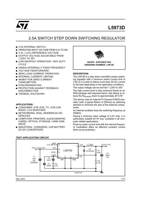
■ 2.5A INTERNAL SWITCH<br />
■ OPERATING INPUT VOLTAGE FROM 4.4V TO 36V<br />
■ 3.3V / (±2%) REFERENCE VOLTAGE<br />
■ OUTPUT VOLTAGE ADJUSTABLE FROM<br />
1.235V TO 35V<br />
■ LOW DROPOUT OPERATION: 100% DUTY<br />
CYCLE<br />
■ 250KHz INTERNALLY FIXED FREQUENCY<br />
■ VOLTAGE FEEDFORWARD<br />
■ ZERO LOAD CURRENT OPERATION<br />
■ INTERNAL CURRENT LIMITING<br />
■ INHIBIT FOR ZERO CURRENT<br />
CONSUMPTION<br />
■ SYNCHRONIZATION<br />
■ PROTECTION AGAINST FEEDBACK<br />
DISCONNECTION<br />
■ THERMAL SHUTDOWN<br />
APPLICATIONS:<br />
■ CONSUMER: STB, DVD, TV, VCR,CAR<br />
RADIO, LCD MONITORS<br />
■ NETWORKING: XDSL, MODEMS,DC-DC<br />
MODULES<br />
■ COMPUTER: PRINTERS, AUDIO/GRAPHIC<br />
CARDS, OPTICAL STORAGE, HARD DISK<br />
DRIVE<br />
■ INDUSTRIAL: CHARGERS, CAR BATTERY<br />
DC-DC CONVERTERS<br />
May 2003<br />
HSOP8 - EXPOSED PAD<br />
ORDERING NUMBER: <strong>L5973D</strong><br />
<strong>L5973D</strong><br />
2.5A SWITCH STEP DOWN SWITCHING REGULATOR<br />
TEST APPLICATION CIRCUIT<br />
VIN = 4.4V to 35V<br />
C1<br />
10μF<br />
35V<br />
CERAMIC<br />
VREF<br />
3.3V<br />
C4<br />
22nF<br />
C3<br />
220pF<br />
VCC<br />
SYNC.<br />
COMP<br />
R3<br />
4.7K<br />
6<br />
8<br />
2<br />
4<br />
INH<br />
<strong>L5973D</strong><br />
3<br />
DESCRIPTION<br />
The <strong>L5973D</strong> is a step down monolithic power switching<br />
regulator with a minimum switch current limit of<br />
2.5A so it is able to deliver more than 2A DC current<br />
to the load depending on the application conditions.<br />
The output voltage can be set from 1.235V to 35V.<br />
The high current level is also achieved thanks to an<br />
SO8 package with exposed frame, that allows to reduce<br />
the Rth(j-amb) down to approximately 40°C/W<br />
The device uses an internal P-Channel D-MOS transistor<br />
(with a typical Rdson of 250mΩ) as switching<br />
element to minimize the size of the external components.<br />
An internal oscillator fixes the switching frequency at<br />
250KHz.<br />
Having a minimum input voltage of 4.4V only, it is<br />
particularly suitable for 5V bus, available in all computer<br />
related applications.<br />
Pulse by pulse current limit with the internal frequency<br />
modulation offers an effective constant current<br />
short circuit protection.<br />
1<br />
5<br />
7<br />
GND<br />
OUT<br />
FB<br />
D03IN1439<br />
L1 15μH<br />
D1<br />
STPS340U<br />
R1<br />
5.6K<br />
R2<br />
3.3K<br />
VOUT=3.3V<br />
C2<br />
330μF<br />
10V<br />
1/10
<strong>L5973D</strong><br />
PIN CONNECTION<br />
PIN DESCRIPTION<br />
THERMAL DATA<br />
(*) Package mounted on board<br />
ABSOLUTE MAXIMUM RATINGS<br />
2/10<br />
N° Pin Function<br />
1 OUT Regulator Output.<br />
2 SYNC Master/slave synchronization.<br />
3 INH A logical signal (active high) disables the device. If INH not used the pin must be grounded.<br />
When it is open an internal pull-up disable the device.<br />
4 COMP E/A output for frequency compensation.<br />
5 FB Feedback input. Connecting directly to this pin results in an output voltage of 1.23V. An external<br />
resistive divider is required for higher output voltages.<br />
6 VREF 3.3V VREF. No cap is requested for stability.<br />
7 GND Ground.<br />
8 VCC Unregulated DC input voltage.<br />
Symbol Parameter Value Unit<br />
Rth (j-amb) Thermal Resistance Junction to ambient Max. 40 (*) °C/W<br />
Symbol Parameter Value Unit<br />
V8 Input Voltage 40 V<br />
V1<br />
OUT<br />
SYNC<br />
INH<br />
COMP<br />
Output DC voltage<br />
Output peak voltage at t = 0.1μs<br />
1<br />
2<br />
3<br />
4<br />
D98IN955<br />
-1 to 40<br />
-5 to 40<br />
I1 Maximum output current int. limit.<br />
V4, V5 Analog pins 4 V<br />
V3 INH -0.3V to VCC<br />
V2 SYNC -0.3 to 4 V<br />
Ptot Power dissipation at Tamb ≤ 60°C 2.25 W<br />
Tj Operating junction temperature range -40 to 150 °C<br />
Tstg Storage temperature range -55 to 150 °C<br />
8<br />
7<br />
6<br />
5<br />
VCC<br />
GND<br />
VREF<br />
FB<br />
V<br />
V
<strong>L5973D</strong><br />
ELECTRICAL CHARACTERISTICS (Tj = 25°C, VCC = 12V, unless otherwise specified.)<br />
(*) Specification Referred to Tj from -40 to 125°C (1) .<br />
Symbol Parameter Test Condition Min. Typ. Max. Unit<br />
VCC Operating input voltage range Vo = 1.235V; Io = 2A * 4.4 36 V<br />
RDSON Mosfet on Resistance * 0.150 0.5 Ω<br />
Il Maximum limiting current VCC = 4.4V to 36V 2.5 3 3.5 A<br />
fs Switching frequency * 212 250 280 KHz<br />
225 250 275 KHz<br />
Duty cycle 0 100 %<br />
DYNAMIC CHARACTERISTICS (see test circuit ).<br />
V5 Voltage feedback 4.4V < VCC < 36V,<br />
1.220 1.235 1.25 V<br />
20mA < IO < 2A<br />
* 1.198 1.235 1.272 V<br />
η Efficiency VO = 5V, VCC = 12V 90 %<br />
DC CHARACTERISTICS<br />
Iqop Total Operating Quiescent<br />
Current<br />
* 3 5 mA<br />
Iq Quiescent current Duty Cycle = 0; VFB = 1.5V 2.5 mA<br />
Iqst-by Total stand-by quiescent current Vinh > 2.2V * 50 100 μA<br />
INHIBIT<br />
VCC = 36V; Vinh > 2.2V * 80 150 μA<br />
INH Threshold Voltage Device ON 0.8 V<br />
Device OFF 2.2 V<br />
ERROR AMPLIFIER<br />
VOH High level output voltage VFB = 1V 3.5 V<br />
VOL Low level output voltage VFB = 1.5V 0.4 V<br />
Io source Source output current VCOMP = 1.9V; VFB = 1V 200 300 μA<br />
Io sink Sink output current VCOMP = 1.9V; VFB = 1.5V 1 1.5 mA<br />
Ib Source bias current 2.5 4 μA<br />
DC open loop gain RL = ∞ 50 57 dB<br />
gm Transconductance Icomp = -0.1mA to 0.1mA<br />
VCOMP = 1.9V<br />
2.3 mS<br />
SYNC FUNCTION<br />
High Input Voltage VCC = 4.4V to 36V 2.5 VREF V<br />
Low Input Voltage VCC = 4.4V to 36V 0.74 V<br />
Slave Sink Current Vsync = 0.74V<br />
0.11<br />
0.25 mA<br />
Vsync = 2.33V<br />
0.21<br />
0.45 mA<br />
Master Output Amplitude Isource = 3mA 2.75 3 V<br />
Output Pulse Width<br />
REFERENCE SECTION<br />
no load, Vsync = 1.65V 0.20 0.35 μs<br />
Reference Voltage 3.234 3.3 3.366 V<br />
IREF = 0 to 5mA<br />
VCC = 4.4V to 36V<br />
* 3.2 3.3 3.399 V<br />
Line Regulation IREF = 0mA<br />
VCC = 4.4V to 36V<br />
5 10 mV<br />
Load Regulation IREF = 0 to 5mA 8 15 mV<br />
Short Circuit Current 10 8 30 mA<br />
Notes: 1. Specification over the -40 to +125 Tj Temperature range are assured by design, characterization and statistical correlation.<br />
2. Guaranteed by design.<br />
3/10
<strong>L5973D</strong><br />
Figure 1. Line Regulation<br />
Vo (V)<br />
3.312<br />
3.308<br />
3.304<br />
3.3<br />
3.296<br />
3.292<br />
3.288<br />
3.284<br />
3.28<br />
3.276<br />
Figure 2. Output Voltage vs. Junction<br />
Temperature<br />
Vo (V)<br />
1.25<br />
1.24<br />
1.23<br />
1.22<br />
1.21<br />
1.2<br />
Figure 3. Quiescent Current vs. Junction<br />
Temperature<br />
4/10<br />
Vcc = 12V<br />
Vo = 3.3V<br />
Tj = 25°C<br />
Tj = 125°C<br />
0 10 20 30 40<br />
Vcc (V)<br />
Vcc = 12V<br />
Vcc=12V<br />
-50 0 50<br />
Tj (°C)<br />
100 150<br />
Iq (mA)<br />
2<br />
1.8<br />
1.6<br />
1.4<br />
1.2<br />
Vcc = 12V<br />
DC = 0%<br />
-50 0 50 100 150<br />
Tj (°C)<br />
Figure 4. Shutdown Current vs.Junction<br />
Temperature<br />
Ishd (μA)<br />
70<br />
60<br />
50<br />
40<br />
30<br />
Vcc = 12V<br />
-50 0 50<br />
Tj (°C)<br />
100 150<br />
Figure 5. Switching Frequency vs.Junction<br />
Temperature<br />
Fsw (KHz)<br />
260<br />
250<br />
240<br />
230<br />
220<br />
Vcc = 12V<br />
Vo = 3.3V<br />
-50 0 50 100 150<br />
Tj (°C)
APPLICATION CIRCUIT<br />
<strong>L5973D</strong><br />
In figure 6 is shown the demo board application circuit, where the input supply voltage, Vcc, can range from 4.4V<br />
to 25V due to the rated voltage of the input capacitor and the output voltage is adjustable from 1.235V to Vcc.<br />
Figure 6. Demo board Application Circuit<br />
VIN = 4.4V to 25V<br />
C1<br />
10μF<br />
25V<br />
CERAMIC<br />
Table 1. Component List<br />
3.3V<br />
C4<br />
22nF<br />
C3<br />
220pF<br />
VREF<br />
VCC<br />
SYNC.<br />
COMP<br />
R3<br />
4.7K<br />
6<br />
8<br />
2<br />
4<br />
INH<br />
<strong>L5973D</strong><br />
3<br />
D03IN1440<br />
Reference Part Number Description Manufacturer<br />
C1 10μF, 25V TOKIN<br />
C2 POSCAP 6TPB330M 330μF, 6.3V Sanyo<br />
C3 C1206C221J5GAC 220pF, 5%, 50V KEMET<br />
C4 C1206C223K5RAC 22nF, 10%, 50V KEMET<br />
R1 5.6K, 1%, 0.1W 0603 Neohm<br />
R2 3.3K, 1%, 0.1W 0603 Neohm<br />
R3 4.7K, 1%, 0.1W 0603 Neohm<br />
D1 STPS2L25U 2A, 25V ST<br />
L1 DO3316P-153 15μH, 3A COILCRAFT<br />
7<br />
GND<br />
1<br />
5<br />
OUT<br />
FB<br />
L1 15μH<br />
D1<br />
STPS2L25U<br />
R1<br />
5.6K<br />
R2<br />
3.3K<br />
VOUT=3.3V<br />
C2<br />
330μF<br />
6.3V<br />
5/10
<strong>L5973D</strong><br />
Figure 7. PCB layout (component side)<br />
Figure 8. PCB layout (bottom side)<br />
Figure 9. PCB layout (front side)<br />
Below some graphs show the Tj versus output current in different conditions of the input and output voltage and<br />
some efficiency measurements.<br />
6/10<br />
42mm<br />
34mm
Figure 10. Junction Temperature vs. Output<br />
Current (VCC = 5V)<br />
Tj(°C)<br />
120<br />
110<br />
100<br />
90<br />
80<br />
70<br />
60<br />
50<br />
40<br />
30<br />
20<br />
Vin=5V<br />
Tamb=25°C<br />
Vo=3.3V<br />
Vo=2.5V<br />
Vo=1.8V<br />
0.2 0.4 0.6 0.8 1 1.2 1.4 1.6 1.8<br />
Io(A)<br />
2 2.2 2.4 2.6<br />
Figure 11. Junction Temperature vs. Output<br />
Current (VCC = 12V)<br />
Tj (°C)<br />
120<br />
110<br />
100<br />
90<br />
80<br />
70<br />
60<br />
50<br />
40<br />
30<br />
20<br />
Vin=12V<br />
Tamb=25°C<br />
Vo=5V<br />
Vo=3.3V<br />
Vo=2.5V<br />
0.2 0.4 0.6 0.8 1 1.2 1.4 1.6 1.8 2 2.2 2.4 2.6<br />
Io (A)<br />
Figure 12. Efficiency vs. Output Current<br />
(VCC = 5V)<br />
Efficiency (%)<br />
95<br />
93<br />
91<br />
89<br />
87<br />
85<br />
83<br />
81<br />
79<br />
77<br />
75<br />
73<br />
71<br />
69<br />
67<br />
Vcc=5V<br />
Vo=2.5V<br />
Vo=1.8V<br />
Vo=3.3V<br />
Figure 13. Efficiency vs. Output Current<br />
(VCC = 12V)<br />
Efficiency (%)<br />
91<br />
89<br />
87<br />
85<br />
83<br />
81<br />
79<br />
77<br />
75<br />
<strong>L5973D</strong><br />
0.1 0.3 0.5 0.7 0.9 1.1 1.3 1.5 1.7 1.9 2.1 2.3<br />
Io (A)<br />
Vo=5V<br />
Vo=3.3V<br />
Vo=2.5V<br />
73<br />
71<br />
69<br />
67<br />
Vcc=12V<br />
65<br />
0.1 0.3 0.5 0.7 0.9 1.1 1.3 1.5 1.7 1.9 2.1 2.3<br />
Io (A)<br />
7/10
<strong>L5973D</strong><br />
APPLICATION IDEAS<br />
Figure 14. Positive Buck-Boost regulator<br />
VIN=5V<br />
C1<br />
10uF<br />
10V<br />
Ceramic<br />
Figure 15. Buck-Boost regulator<br />
Figure 16. Dual output voltage with auxiliary winding<br />
8/10<br />
VIN=5V<br />
C1<br />
10uF<br />
10V<br />
Ceramic<br />
VIN=12V<br />
C1<br />
10uF<br />
25V<br />
Ceramic<br />
C2<br />
220pF<br />
C3<br />
22nF<br />
R3<br />
4.7k<br />
C2<br />
10uF<br />
25V<br />
Ceramic<br />
C2<br />
220pF<br />
Vcc<br />
COMP<br />
C3<br />
220pF<br />
C3<br />
22nF<br />
R3<br />
4.7k<br />
8<br />
4<br />
2<br />
SYNC VREF<br />
VCC<br />
COMP<br />
C4<br />
22nF<br />
R3<br />
4.7k<br />
8<br />
<strong>L5973D</strong><br />
6<br />
3.3V<br />
Vcc<br />
COMP<br />
4<br />
2<br />
SYNC VREF<br />
GND<br />
8<br />
7<br />
4<br />
2<br />
1<br />
5<br />
3<br />
SYNC VREF<br />
<strong>L5973D</strong><br />
6<br />
3.3V<br />
GND<br />
7<br />
INH<br />
OUT<br />
FB<br />
<strong>L5973D</strong><br />
6<br />
3.3V<br />
GND<br />
1<br />
5<br />
3<br />
INH<br />
D1<br />
STPS2L25U<br />
7<br />
OUT<br />
FB<br />
1<br />
5<br />
3<br />
INH<br />
OUT<br />
FB<br />
L1<br />
15uH<br />
2.7k<br />
24k<br />
N1/N2=2<br />
D1<br />
STPS25L25U<br />
M1<br />
STN4NE03L<br />
D1<br />
STPS2L25U<br />
C5<br />
100uF<br />
16V<br />
D2<br />
1N4148<br />
Lp=22uH<br />
D2<br />
STPS2L25U<br />
L1<br />
15uH<br />
24k<br />
2.7k<br />
C4<br />
100uF<br />
10V<br />
VOUT=12V/0.6A<br />
C4<br />
100uF<br />
16V<br />
VOUT=-12V/0.6A<br />
VOUT1=5V<br />
50mA<br />
VOUT=3.3V<br />
0.5A<br />
C5<br />
47uF<br />
10V
DIM.<br />
mm inch<br />
MIN. TYP. MAX. MIN. TYP. MAX.<br />
A 1.350 1.750 0.531 0.069<br />
A1<br />
A2<br />
B<br />
C<br />
D<br />
E<br />
e<br />
H<br />
h<br />
L<br />
0.100 0.250 0.004 0.010<br />
1.100 1.650 0.043 0.065<br />
0.330 0.510 0.013 0.020<br />
0.190 0.250 0.07 0.010<br />
4.800 5.000 0.189 0.197<br />
3.800 4.000 0.150 0.157<br />
1.270 0.05<br />
5.800 6.200 0.228 0.244<br />
0.250 0.500 0.010 0.020<br />
0.400 1.270 0.016 0.05<br />
k 0˚ (min), 8˚ (max)<br />
ddd 0.100 0.010<br />
(1) Dimension D does not include mold flash, protusions<br />
or gate burrs shall not exeed 0.15mm (both side).<br />
Exposed Pad:<br />
D1 = 3.1mm<br />
E1 = 2.41mm<br />
OUTLINE AND<br />
MECHANICAL DATA<br />
HSOP8<br />
(Exposed Pad)<br />
<strong>L5973D</strong><br />
7195016<br />
9/10
<strong>L5973D</strong><br />
Information furnished is believed to be accurate and reliable. However, STMicroelectronics assumes no responsibility for the consequences<br />
of use of such information nor for any infringement of patents or other rights of third parties which may result from its use. No license is granted<br />
by implication or otherwise under any patent or patent rights of STMicroelectronics. Specifications mentioned in this publication are subject<br />
to change without notice. This publication supersedes and replaces all information previously supplied. STMicroelectronics products are not<br />
authorized for use as critical components in life support devices or systems without express written approval of STMicroelectronics.<br />
The ST logo is a registered trademark of STMicroelectronics<br />
® 2003 STMicroelectronics - All Rights Reserved<br />
STMicroelectronics GROUP OF COMPANIES<br />
Australia - Brazil - Canada - China - Finland - France - Germany - Hong Kong - India - Israel - Italy - Japan -Malaysia - Malta - Morocco -<br />
Singapore - Spain - Sweden - Switzerland - United Kingdom - United States.<br />
http://www.st.com<br />
10/10