
Create successful ePaper yourself
Turn your PDF publications into a flip-book with our unique Google optimized e-Paper software.
®<br />
High output power : PO = 10 + 10 W@RL = 2Ω, d =<br />
10% ; PO = <strong>20W</strong>@RL = 4Ω , d = 1 %.<br />
High reliability of the chip and package with addi-<br />
.<br />
tional complete safety during operation thanks to<br />
protection against :<br />
.<br />
OUTPUT DC AND AC SHORT CIRCUIT TO<br />
.<br />
GROUND<br />
.<br />
OVERRATING CHIP TEMPERATURE<br />
.<br />
LOAD DUMP VOLTAGE SURGE<br />
<strong>FOR</strong>TUITOUS OPEN GROUND<br />
VERY INDUCTIVE LOADS<br />
Flexibility in use : bridge or stereo booster amplifiers<br />
with or without boostrap and with programmable<br />
gain and bandwidth.<br />
Space and cost saving : very low number of external<br />
components, very simple mounting system with<br />
no electrical isolation between the package and the<br />
heatsink (one screw only).<br />
In addition, the circuit offers loudspeaker protection<br />
during short circuit for one wire to ground.<br />
ABSOLUTE MAXIMUM RATINGS<br />
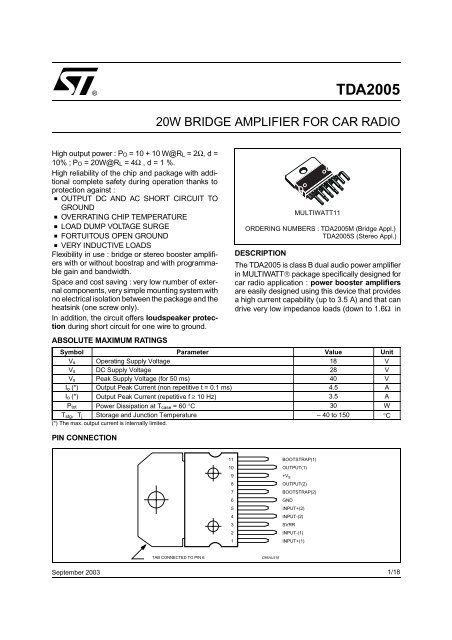
PIN CONNECTION<br />
September 2003<br />
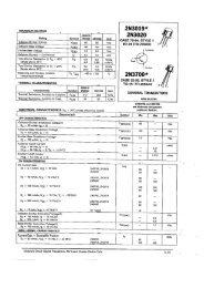
TDA2005<br />
<strong>20W</strong> <strong>BRIDGE</strong> <strong>AMPLIFIER</strong> <strong>FOR</strong> <strong>CAR</strong> <strong>RADIO</strong><br />
TAB CONNECTED TO PIN 6 D95AU318<br />
11<br />
10<br />
9<br />
8<br />
7<br />
6<br />
5<br />
4<br />
3<br />
2<br />
1<br />
BOOTSTRAP(1)<br />
OUTPUT(1)<br />
+V S<br />
OUTPUT(2)<br />
BOOTSTRAP(2)<br />
GND<br />
INPUT+(2)<br />
INPUT-(2)<br />
SVRR<br />
INPUT-(1)<br />
INPUT+(1)<br />
MULTIWATT11<br />
ORDERING NUMBERS : TDA2005M (Bridge Appl.)<br />
TDA2005S (Stereo Appl.)<br />
DESCRIPTION<br />
The TDA2005 is class B dual audio power amplifier<br />
in MULTIWATT® package specifically designed for<br />
car radio application : power booster amplifiers<br />
are easily designed using this device that provides<br />
a high current capability (up to 3.5 A) and that can<br />
drive very low impedance loads (down to 1.6Ω in<br />
Symbol Parameter Value Unit<br />
Vs Operating Supply Voltage 18 V<br />
Vs DC Supply Voltage 28 V<br />
Vs Peak Supply Voltage (for 50 ms) 40 V<br />
Io (*) Output Peak Current (non repetitive t = 0.1 ms) 4.5 A<br />
Io (*) Output Peak Current (repetitive f ≥ 10 Hz) 3.5 A<br />
Ptot Power Dissipation at Tcase = 60 °C 30 W<br />
Tstg, Tj Storage and Junction Temperature – 40 to 150 °C<br />
(*) The max. output current is internally limited.<br />
1/18
TDA2005<br />
SCHEMATIC DIAGRAM<br />
THERMAL DATA<br />
2/18<br />
Symbol Parameter Value Unit<br />
Rth j-case Thermal Resistance Junction-case Max. 3 °C/W
<strong>BRIDGE</strong> <strong>AMPLIFIER</strong> APPLICATION (TDA2005M)<br />
Figure 1 : Test and Application Circuit (Bridge amplifier)<br />
Figure 2 : P.C. Board and Components Layout of Figure 1 (1:1 scale)<br />
TDA2005<br />
3/18
TDA2005<br />
ELECTRICAL CHARACTERISTICS (refer to the Bridge application circuit, Tamb = 25 o C, GV = 50dB,<br />
Rth (heatsink) = 4 o C/W, unless otherwise specified)<br />
Symbol Parameter Test Conditions Min. Typ. Max. Unit<br />
Vs Supply Voltage 8 18 V<br />
Vos Output Offset Voltage (1)<br />
(between pin 8 and pin 10)<br />
Vs = 14.4V<br />
Vs = 13.2V<br />
150<br />
150<br />
mV<br />
mV<br />
Id Total Quiescent Drain Current Vs = 14.4V<br />
Vs = 13.2V<br />
RL = 4Ω<br />
RL = 3.2Ω<br />
75<br />
70<br />
150<br />
160<br />
mA<br />
mA<br />
Po Output Power d = 10%<br />
Vs = 14.4V<br />
Vs = 13.2V<br />
f = 1 Hz<br />
RL = 4Ω<br />
RL = 3.2Ω<br />
RL = 3.2 Ω<br />
18<br />
20<br />
17<br />
20<br />
22<br />
19<br />
W<br />
d Distortion f = 1kHz<br />
Vs = 14.4V RL = 4Ω<br />
Po = 50mW to 15W<br />
Vs = 13.2V RL = 3.2Ω<br />
Po = 50mW to 13W<br />
1<br />
1<br />
%<br />
%<br />
Vi Input Sensitivity f = 1kHz<br />
Po = 2W<br />
Po = 2W<br />
RL = 4Ω<br />
RL = 3.2Ω<br />
9<br />
8<br />
mV<br />
mV<br />
Ri Input Resistance f = 1kHz 70 kΩ<br />
fL Low Frequency Roll Off (– 3dB) RL = 3.2Ω 40 Hz<br />
fH High Frequency Roll Off (– 3dB) RL = 3.2Ω 20 kHz<br />
Gv Closed Loop Voltage Gain f = 1kHz 50 dB<br />
eN Total Input Noise Voltage Rg = 10kΩ (2) 3 10 μV<br />
SVR Supply Voltage Rejection Rg = 10kΩ, C4 = 10μF<br />
fripple = 100Hz, Vripple = 0.5V<br />
45 55 dB<br />
h Efficiency Vs = 14.4V, f = 1 kHz<br />
Po = <strong>20W</strong> RL = 4Ω<br />
Po = 22W RL = 3.2Ω<br />
Vs = 13.2V, f = 1 kHz<br />
Po = 19W RL = 3.2Ω<br />
60<br />
60<br />
58<br />
%<br />
%<br />
%<br />
Tj Thermal Shut-down Junction<br />
Temperature<br />
Vs = 14.4V, RL = 4Ω<br />
f = 1kHz, Ptot = 13W<br />
145 °C<br />
VOSH Output Voltage with one Side of<br />
the Speaker shorted to ground<br />
Vs = 14.4V<br />
Vs = 13.2V<br />
RL = 4Ω<br />
RL = 3.2Ω 2 V<br />
Notes : 1. For TDA2005M only<br />
2. Bandwith Filter : 22Hz to 22kHz.<br />
4/18
Figure 3 : Output Offset Voltage versus<br />
Supply Voltage<br />
Figure 5 : Distortion versus Output Power<br />
(bridge amplifier)<br />
<strong>BRIDGE</strong> <strong>AMPLIFIER</strong> DESIGN<br />
The following consideraions can be useful when designing a bridge amplifier.<br />
Vo max<br />
Io max<br />
Po max<br />
Parameter Single Ended Bridge<br />
Peak Output Voltage (before clipping)<br />
1<br />
2 (Vs – 2 VCE sat) Vs – 2 VCE sat<br />
Peak Output Current (before clippling)<br />
RMS Output Power (before clipping)<br />
Where : VCE sat = output transistors saturation voltage<br />
VS = allowable supply voltage<br />
RL = load impedance<br />
Figure 4 : Distortion versus Output Power<br />
(bridge amplifier)<br />
1<br />
2 VS − 2 VCE sat<br />
RL<br />
1<br />
4 (VS − 2 VCE sat) 2<br />
2 RL<br />
VS − 2 VCE sat<br />
RL<br />
(VS − 2 VCE sat) 2<br />
2 RL<br />
TDA2005<br />
5/18
TDA2005<br />
Voltage and current swings are twice for a bridge<br />
amplifier in comparison with single ended amplifier.<br />
In order words, with the same RL the bridge configuration<br />
can deliver an output power that is four<br />
times the output power of a single ended amplifier,<br />
while, with the same max output current the bridge<br />
configuration can deliver an output power that is<br />
twice the output power of a single ended amplifier.<br />
Core must be taken when selecting VS and RL in<br />
order to avoid an output peak current above the<br />
absolute maximum rating.<br />
From the expression for IO max, assuming VS<br />
= 14.4V and VCE sat = 2V, the minimum load that<br />
can be driven by TDA2005 in bridge configuration<br />
is :<br />
RL min = VS − 2 VCEsat<br />
IO max<br />
= 14.4 −4<br />
3.5<br />
= 2.97Ω<br />
The voltage gain of the bridge configuration is given<br />
by (see Figure 34) :<br />
GV = V0<br />
= 1 +<br />
V1<br />
⎛<br />
⎜<br />
⎝<br />
R1<br />
R2 ⋅ R4<br />
R2 + R4<br />
⎞ ⎟ ⎠<br />
+ R3<br />
R4<br />
STEREO <strong>AMPLIFIER</strong> APPLICATION (TDA2005S)<br />
Figure 7 : Typical Application Circuit<br />
6/18<br />
For sufficiently high gains (40 to 50dB) it is possible<br />
to put R2 = R4 and R3 = 2 R1, simplifing the formula<br />
in :<br />
GV = 4 R1<br />
R2<br />
Gv (dB) R1 (Ω) R2 = R4 (Ω) R3 (Ω)<br />
40<br />
50<br />
1000<br />
1000<br />
Figure 6 : Bridge Configuration<br />
39<br />
12<br />
2000<br />
2000
ELECTRICAL CHARACTERISTICS (refer to the Stereo application circuit, Tamb = 25 o C, GV = 50dB,<br />
Rth (heatsink) = 4 o C/W, unless otherwwise specified)<br />
Symbol Parameter Test Conditions Min. Typ. Max. Unit<br />
Vs Supply Voltage 8 18 V<br />
Vo Quiescent Output Voltage Vs = 14.4V<br />
Vs = 13.2V<br />
6.6<br />
6<br />
7.2<br />
6.6<br />
7.8<br />
7.2<br />
V<br />
V<br />
Id Total Quiescent Drain Current Vs = 14.4V<br />
Vs = 13.2V<br />
65<br />
62<br />
120<br />
120<br />
mA<br />
mA<br />
Po Output Power (each channel) f = 1kHz, d = 10%<br />
Vs = 14.4V RL = 4Ω<br />
RL = 3.2Ω<br />
RL = 2Ω<br />
RL = 1.6Ω<br />
Vs = 13.2V RL = 3.2Ω<br />
RL = 1.6Ω<br />
Vs = 16V RL = 2Ω<br />
6<br />
7<br />
9<br />
10<br />
69<br />
6.5<br />
8<br />
10<br />
11<br />
6.5<br />
10<br />
12<br />
W<br />
d Distortion (each channel) f = 1kHz<br />
Vs = 14.4V RL = 4Ω<br />
Po = 50mW to 4W<br />
Vs = 14.4V RL = 2Ω<br />
Po = 50mW to 6W<br />
Vs = 13.2V RL = 3.2Ω<br />
Po = 50mW to 3W<br />
Vs = 13.2V RL = 1.6Ω<br />
Po = 40mW to 6W<br />
CT Cross Talk (1) Vs = 14.4V, Vo = 4VRMS<br />
RL = 4Ω, Rg = 5kΩ<br />
f = 1kHz<br />
f = 10kHz<br />
Vi Input Saturation Voltage 300 mV<br />
Vi Input Sensitivity f = 1kHz, Po = 1W<br />
RL = 4Ω<br />
RL = 3.2Ω<br />
Ri Input Resistance f = 1kHz 70 200 kΩ<br />
fL Low Frequency Roll Off (– 3dB) RL = 2Ω 50 Hz<br />
fH High Frequency Roll Off (– 3dB) RL = 2Ω 15 kHz<br />
Gv Voltage Gain (open loop) f = 1kHz 90 dB<br />
Gv Voltage Gain (closed loop) f = 1kHz 48 50 51 dB<br />
D Gv Closed Loop Gain Matching 0.5 dB<br />
eN Total Input Noise Voltage Rg = 10kΩ (2) 1.5 5 μV<br />
SVR Supply Voltage Rejection Rg = 10kΩ, C3 = 10μF<br />
fripple = 100Hz, Vripple = 0.5V<br />
35 45 dB<br />
h Efficiency Vs = 14.4V, f = 1kHz<br />
Po = 6.5W RL = 4Ω<br />
Po = 10W RL = 2Ω<br />
Vs = 13.2V, f = 1kHz<br />
Po = 6.5W RL = 3.2Ω<br />
Po = 100W RL = 1.6Ω<br />
70<br />
60<br />
70<br />
60<br />
%<br />
%<br />
%<br />
%<br />
Notes : 1. For TDA2005M only<br />
2. Bandwith Filter : 22Hz to 22kHz.<br />
0.2<br />
0.3<br />
0.2<br />
0.3<br />
60<br />
45<br />
6<br />
5.5<br />
TDA2005<br />
1<br />
1<br />
1<br />
1<br />
%<br />
%<br />
%<br />
%<br />
dB<br />
mV<br />
7/18
TDA2005<br />
Figure 8 : Quiescent Output Voltage versus<br />
Supply Voltage (Stereo amplifier)<br />
Figure 10 : Distortion versus Output Power<br />
(Stereo amplifier)<br />
Figure 12 : Output Power versus Supply Voltage<br />
(Stereo amplifier)<br />
8/18<br />
Figure 9 : Quiescent Drain Current versus<br />
Supply Voltage (Stereo amplifier)<br />
Figure 11 : Output Power versus Supply Voltage<br />
(Stereo amplifier)<br />
Figure 13 : Distortion versus Frequency<br />
(Stereo amplifier)
Figure 14 : Distortion versus Frequency<br />
(Stereo amplifier)<br />
Figure 16 : Supply Voltage Rejection versus<br />
Frequency (Stereo amplifier)<br />
Figure 18 : Supply Voltage Rejection versus<br />
C2 and C3 (Stereo amplifier)<br />
Figure 15 : Supply Voltage Rejection versus C3<br />
(Stereo amplifier)<br />
Figure 17 : Supply Voltage Rejection versus<br />
C2 and C3 (Stereo amplifier)<br />
Figure 19 : Gain versus Input Sensitivity<br />
(Stereo amplifier)<br />
TDA2005<br />
9/18
TDA2005<br />
Figure 20 : Gain versus Input Sensitivity<br />
(Stereo amplifier)<br />
Figure 22 : Total Power Dissipation and Efficiency<br />
versus Output Power<br />
(Stereo amplifier)<br />
10/18<br />
Figure 21 : Total Power Dissipation and Efficiency<br />
versus Output Power<br />
(Bridge amplifier)
APPLICATION SUGGESTION<br />
The recommended values of the components are those shown on Bridge applicatiion circuit of Figure 1.<br />
Different values can be used ; the following table can help the designer.<br />
Comp. Recom.<br />
Value<br />
R1 120 kΩ Optimization of the Output<br />
Symmetry<br />
R2 1kΩ<br />
R3 2 kΩ<br />
R4, R5 12 Ω Closed Loop Gain Setting (see<br />
Bridge Amplifier Design) (*)<br />
Purpose Larger Than Smaller Than<br />
Smaller Po max<br />
R6, R7 1 Ω Frequency Stability Danger of Oscillation at High<br />
Frequency with Inductive Loads<br />
C1 2.2 μF Input DC Decoupling<br />
C2 2.2 μF Optimization of Turn on Pop and<br />
Turn on Delay<br />
Smaller Po max<br />
High Turn on Delay Higher Turn on Pop, Higher<br />
Low Frequency Cut-off,<br />
Increase of Noise<br />
C3 0.1 μF Supply by Pass Danger of Oscillation<br />
C4 10 μF Ripple Rejection Increase of SVR, Increase of<br />
the Switch-on Time<br />
Degradation of SVR.<br />
C5, C7 100 μF Bootstrapping Increase of Distortion<br />
at low Frequency<br />
C6, C8 220 μF Feedback Input DC Decoupling,<br />
Low Frequency Cut-off<br />
Higher Low Frequency<br />
Cut-off<br />
C9, C10 0.1 μF Frequency Stability Danger of Oscillation<br />
(*) The closed loop gain must be higher than 32dB.<br />
TDA2005<br />
11/18
TDA2005<br />
APPLICATION IN<strong>FOR</strong>MATION<br />
Figure 23 : Bridge Amplifier without Boostrap<br />
Figure 24 : P.C. Board and Components Layout of Figure 23 (1:1 scale)<br />
12/18
APPLICATION IN<strong>FOR</strong>MATION (continued)<br />
Figure 25 : Low Cost Bridge Amplifier (GV = 42dB)<br />
Figure 26 : P.C. Board and Components Layout of Figure 25 (1:1 scale)<br />
TDA2005<br />
13/18
TDA2005<br />
APPLICATION IN<strong>FOR</strong>MATION (continued)<br />
Figure 27 : 10 + 10 W Stereo Amplifier with Tone Balance and Loudness Control<br />
Figure 28 : Tone Control Response<br />
(circuit of Figure 29)<br />
14/18
APPLICATION IN<strong>FOR</strong>MATION (continued)<br />
Figure 29 : <strong>20W</strong> Bus Amplifier<br />
Figure 30 : Simple <strong>20W</strong> Two Way Amplifier (FC = 2kHz)<br />
TDA2005<br />
15/18
TDA2005<br />
APPLICATION IN<strong>FOR</strong>MATION (continued)<br />
Figure 31 : Bridge Amplifier Circuit suited for Low-gain Applications (GV = 34dB)<br />
Figure 32 : Example of Muting Circuit<br />
16/18
BUILT-IN PROTECTION SYSTEMS<br />
Load Dump Voltage Surge<br />
The TDA2005 has a circuit which enables it to<br />
withstand a voltage pulse train, on Pin 9, of the type<br />
shown in Figure 34.<br />
If the supply voltage peaks to more than 40V, then<br />
an LC filter must be inserted between the supply<br />
and pin 9, in order to assure that the pulses at pin<br />
9 will be held withing the limits shown.<br />
A suggested LC network is shown in Figure 33. With<br />
this network, a train of pulses with amplitude up to<br />
120V and width of 2ms can be applied at point A.<br />
This type of protection is ON when the supply<br />
voltage (pulse or DC) exceeds 18V. For this reason<br />
the maximum operating supply voltage is 18V.<br />
Figure 33<br />
Figure 34<br />
Short Circuit (AC and DC conditions)<br />
The TDA2005 can withstand a permanent short-circuit<br />
on the output for a supply voltage up to 16V.<br />
Polarity Inversion<br />
High current (up to 10A) can be handled by the<br />
device with no damage for a longer period than the<br />
blow-out time of a quick 2A fuse (normally connected<br />
in series with the supply). This feature is<br />
added to avoid destruction, if during fitting to the<br />
car, a mistake on the connection of the supply is<br />
made.<br />
TDA2005<br />
Open Ground<br />
When the ratio is in the ON condition and the<br />
ground is accidentally opened, a standard audio<br />
amplifier will be damaged. On the TDA2005 protection<br />
diodes are included to avoid any damage.<br />
Inductive Load<br />
A protection diode is provided to allow use of the<br />
TDA2005 with inductive loads.<br />
DC Voltage<br />
The maximum operating DC voltage for the<br />
TDA2005 is 18V.<br />
However the device can withstand a DC voltage up<br />
to 28V with no damage. This could occur during<br />
winter if two batteries are series connected to crank<br />
the engine.<br />
Thermal Shut-down<br />
The presence of a thermal limiting circuit offers the<br />
following advantages :<br />
1) an overload on the output (even if it is<br />
permanent), or an excessive ambient<br />
temperature can be easily withstood.<br />
2) the heatsink can have a smaller factor of safety<br />
compared with that of a conventional circuit.<br />
There is no device damage in the case of<br />
excessive junction temperature : all that<br />
happens is that PO (and therefore Ptot) and Id are<br />
reduced.<br />
The maximum allowable power dissipation depends<br />
upon the size of the external heatsink (i.e. its<br />
thermal resistance) ; Figure 35 shows the dissipable<br />
power as a function of ambient temperature for<br />
different thermal resistance.<br />
Loudspeaker Protection<br />
The circuit offers loudspeaker protection during<br />
short circuit for one wire to ground.<br />
17/18
TDA2005<br />
Figure 35 : Maximum Allowable Power Dissipation<br />
versus Ambient Temperature<br />
Figure 37 : Output Power and Drain Current versus<br />
Case Temperature<br />
18/18<br />
Figure 36 : Output Power and Drain Current versus<br />
Case Temperature
DIM.<br />
MIN.<br />
mm<br />
TYP. MAX. MIN.<br />
inch<br />
TYP. MAX.<br />
A 5 0.197<br />
B 2.65 0.104<br />
C 1.6 0.063<br />
D 1 0.039<br />
E 0.49 0.55 0.019 0.022<br />
F 0.88 0.95 0.035 0.037<br />
G 1.45 1.7 1.95 0.057 0.067 0.077<br />
G1 16.75 17 17.25 0.659 0.669 0.679<br />
H1 19.6 0.772<br />
H2 20.2 0.795<br />
L 21.9 22.2 22.5 0.862 0.874 0.886<br />
L1 21.7 22.1 22.5 0.854 0.87 0.886<br />
L2 17.4 18.1 0.685 0.713<br />
L3 17.25 17.5 17.75 0.679 0.689 0.699<br />
L4 10.3 10.7 10.9 0.406 0.421 0.429<br />
L7 2.65 2.9 0.104 0.114<br />
M 4.25 4.55 4.85 0.167 0.179 0.191<br />
M1 4.73 5.08 5.43 0.186 0.200 0.214<br />
S 1.9 2.6 0.075 0.102<br />
S1 1.9 2.6 0.075 0.102<br />
Dia1 3.65 3.85 0.144 0.152<br />
OUTLINE AND<br />
MECHANICAL DATA<br />
Multiwatt11 V<br />
TDA2005<br />
19/18
TDA2005<br />
Information furnished is believed to be accurate and reliable. However, STMicroelectronics assumes no responsibility for the consequences<br />
of use of such information nor for any infringement of patents or other rights of third parties which may result from its use. No license is granted<br />
by implication or otherwise under any patent or patent rights of STMicroelectronics. Specifications mentioned in this publication are subject to<br />
change without notice. This publication supersedes and replaces all information previously supplied. STMicroelectronics products are not<br />
authorized for use as critical components in life support devices or systems without express written approval of STMicroelectronics.<br />
The ST logo is a registered trademark of STMicroelectronics.<br />
All other names are the property of their respective owners<br />
© 2003 STMicroelectronics - All rights reserved<br />
STMicroelectronics GROUP OF COMPANIES<br />
Australia – Belgium - Brazil - Canada - China – Czech Republic - Finland - France - Germany - Hong Kong - India - Israel - Italy - Japan<br />
- Malaysia - Malta - Morocco - Singapore - Spain - Sweden - Switzerland - United Kingdom - United States<br />
www.st.com<br />
20/18