InAs/(GaIn)Sb short-period superlattices for focal plane arrays
InAs/(GaIn)Sb short-period superlattices for focal plane arrays
InAs/(GaIn)Sb short-period superlattices for focal plane arrays

You also want an ePaper? Increase the reach of your titles
YUMPU automatically turns print PDFs into web optimized ePapers that Google loves.
Copyright 2005 Society of Photo-Optical Instrumentation Engineers<br />
<strong>InAs</strong>/(<strong>GaIn</strong>)<strong>Sb</strong> <strong>short</strong>-<strong>period</strong> <strong>superlattices</strong> <strong>for</strong> <strong>focal</strong> <strong>plane</strong> <strong>arrays</strong><br />
Robert Rehm 1a , Martin Walther a , Johannes Schmitz a , Joachim Fleißner a , Frank Fuchs a ,<br />
Wolfgang Cabanski b , and Johann Ziegler b<br />
a Fraunhofer-Institut für Angewandte Festkörperphysik, Freiburg i. Br., Germany<br />
b AEG Infrarot-Module GmbH (AIM), Heilbronn, Germany<br />
ABSTRACT<br />
An infrared camera based on a 256x256 <strong>focal</strong> <strong>plane</strong> array <strong>for</strong> the Mid-IR spectral range (3-5 µm) has been realized <strong>for</strong><br />
the first time with <strong>InAs</strong>/Ga<strong>Sb</strong> <strong>short</strong>-<strong>period</strong> <strong>superlattices</strong>. The detector shows a cut-off wavelength of 5.4 µm and reveals<br />
a quantum efficiency of 30%. The noise equivalent temperature difference (NETD) reaches 9.4 mK at 73 K with F/2<br />
optics and 6.5 ms integration time. Excellent thermal images with low NETD values and a very good modulation<br />
transfer function are presented. Furthermore, a new method to passivate <strong>InAs</strong>/<strong>GaIn</strong><strong>Sb</strong> superlattice photodiodes <strong>for</strong> the<br />
8-10 µm regime is demonstrated. The approach is based on the epitaxial overgrowth of wet-etched mesa diodes using<br />
lattice matched AlGaAs<strong>Sb</strong>. A complete suppression of surface leakage currents in small sized test diodes with 70 µm<br />
diameter is observed.<br />
Keywords: infrared, <strong>focal</strong> <strong>plane</strong> array, superlattice, Ga<strong>Sb</strong>, thermal imaging<br />
1. INTRODUCTION<br />
In the past years, several groups have demonstrated promising photodiodes based on <strong>InAs</strong>/(<strong>GaIn</strong>)<strong>Sb</strong> <strong>superlattices</strong><br />
[1,2,3]. Since the demonstration of the first fully operational 256x256 Mid-IR (MWIR) camera exhibiting an excellent<br />
per<strong>for</strong>mance [4], the interest in <strong>InAs</strong>/(<strong>GaIn</strong>)<strong>Sb</strong> p-i-n superlattice photodiodes <strong>for</strong> the fabrication of <strong>focal</strong> <strong>plane</strong> <strong>arrays</strong><br />
(FPA) <strong>for</strong> the second (3-5 µm) and third (8-12 µm) atmospheric transmission window has increased strongly. The high<br />
quantum efficiency of p-i-n superlattice photodiodes allows to achieve a very low noise-equivalent temperature<br />
difference at a <strong>short</strong> integration time.<br />
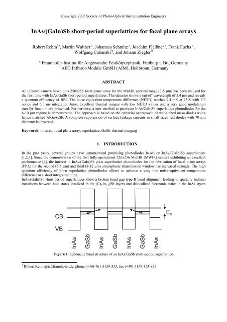
<strong>InAs</strong>/(<strong>GaIn</strong>)<strong>Sb</strong> <strong>short</strong>-<strong>period</strong> <strong>superlattices</strong> show a broken band gap type-II band alignment leading to spatially indirect<br />
transitions between hole states localized in the (GaxIn1-x)<strong>Sb</strong> layers and delocalized electronic states in the <strong>InAs</strong> layers<br />
VB<br />
<strong>InAs</strong><br />
Ga<strong>Sb</strong><br />
<strong>InAs</strong><br />
Ga<strong>Sb</strong><br />
<strong>InAs</strong><br />
Ga<strong>Sb</strong><br />
<strong>InAs</strong><br />
E G<br />
Figure 1. Schematic band structure of an <strong>InAs</strong>/Ga<strong>Sb</strong> <strong>short</strong>-<strong>period</strong> superlattice.<br />
1 Robert.Rehm@iaf.fraunhofer.de, phone (+49)-761-5159-353, fax (+49)-5159-353-851
(see Figure 1). The effective band gap EG of these structures can be adjusted from 0.3 eV to values below 0.1 eV by<br />
varying the thickness of the <strong>InAs</strong> layer or the indium mole fraction in the (GaxIn1-x)<strong>Sb</strong>. The growth is per<strong>for</strong>med by<br />
Molecular Beam Epitaxy (MBE) on 2” Ga<strong>Sb</strong> substrates which are commercially available with low defect densities.<br />
During growth, the strain can be kept sufficiently low by precisely controlling the interfaces between the <strong>InAs</strong> and the<br />
(<strong>GaIn</strong>)<strong>Sb</strong>. The MBE growth process offers promising prospects <strong>for</strong> future dual color / dual band sensors <strong>for</strong> 3 rd<br />
generation thermal imaging.<br />
For the realization of high per<strong>for</strong>mance IR-camera systems, Fraunhofer IAF cooperates with AIM Infrarot Module<br />
GmbH (AIM) located in Heilbronn, Germany. Fraunhofer IAF is committed to the development and fabrication of the<br />
detector chip, i.e., the MBE growth, process technology and electro-optical characterization. IAF’s fully processed<br />
detector chips are hybridized at AIM with a custom-designed silicon readout integrated circuit (ROIC) using flip-chip<br />
indium solder bump technology. These detector hybrids are mounted into a detector cooler assembly with a 1 W linear<br />
Stirling cooler, which is part of a complete IR imaging camera system. Subsequently, an overview of the Fraunhofer<br />
IAF / AIM superlattice technology will be presented.<br />
2. <strong>InAs</strong>/Ga<strong>Sb</strong> SHORT-PERIOD SUPERLATTICES FOR THE MID-IR SPECTRAL RANGE<br />
Sensors <strong>for</strong> the Mid-IR spectral range between 3-5 µm are based on binary <strong>InAs</strong>/Ga<strong>Sb</strong> <strong>short</strong>-<strong>period</strong> <strong>superlattices</strong>. MBE<br />
growth starts with a 500 nm thick Al0.5Ga0.5As0.04<strong>Sb</strong>0.96 lattice matched buffer layer followed by 700 nm Ga<strong>Sb</strong>:Be<br />
(3x10 18 cm -3 ) acting as a p-type contact layer. Subsequently, 190 <strong>period</strong>s of a 9 monolayer (ML) <strong>InAs</strong> / 10 ML Ga<strong>Sb</strong><br />
superlattice are grown. The SL region is terminated by a 20 nm <strong>InAs</strong>:Si (1x10 17 cm -3 ) cap layer representing an ohmic<br />
n-contact layer. For the <strong>for</strong>mation of p-i-n photodiodes the lower 90 <strong>period</strong>s of the SL are p-doped with 1x10 17 cm -3 Be<br />
in the Ga<strong>Sb</strong> layers. The next 40 SL-<strong>period</strong>s are not intentionally doped followed by 60 <strong>period</strong>s with a n-type doping of<br />
1x10 17 cm -3 Si in the <strong>InAs</strong> layers. The tensile strain caused by the lattice mismatch between <strong>InAs</strong> and Ga<strong>Sb</strong>, was<br />
compensated by the <strong>for</strong>mation of In<strong>Sb</strong>-like bonds at the interfaces in the SL by an appropriate shutter sequence during<br />
growth [5]. Growth conditions, i.e. growth temperature, V/III beam equivalent pressure ratios and shutter sequences<br />
have been optimized in order to improve material quality and to establish a reproducible and reliable growth<br />
process [6].<br />
Figure 2. Cross-section schematic of a 9 ML <strong>InAs</strong> / 10 ML Ga<strong>Sb</strong> p-i-n<br />
superlattice photodiode <strong>for</strong> the Mid-IR spectral region.<br />
256 x 256 FPAs with 40 µm pitch are processed as full wafers using standard optical lithography with a mask set which<br />
also contains various test diodes with different size and geometry. On a single 2” Ga<strong>Sb</strong> wafer four FPAs are realized,<br />
each with 11.2 x 11.2 mm 2 area. Processing starts with the deposition of the ohmic n-contact metalization, followed by<br />
a dry etching process <strong>for</strong> mesa definition using Chemically Assisted Ion Beam Etching (CAIBE). Subsequently, the
Figure 3. SEM image of a 256 x 256 MWIR <strong>InAs</strong>/Ga<strong>Sb</strong> superlattice FPA after CAIBE dry etching of the mesas (a)<br />
and at the end of the process prior to hybridization with the silicon ROIC (b).<br />
etch damage is removed by wet chemical means. After the evaporation of the p-contact metalization, the samples are<br />
passivated with a SiO2-based approach. Figure 2 shows a schematic cross-section of a diode after the subsequent<br />
fluorine-based reactive ion etching of the dielectric passivation layer on top of the contact metalization. In Figure 3a, a<br />
scanning electron microscope (SEM) image prior to the deposition of the passivation layer is shown. The high<br />
selectivity of the wet chemical etchant used <strong>for</strong> the etch damage removal produces a small step between the Ga<strong>Sb</strong>:Be ptype<br />
contact layer and the superlattice. After the deposition of further metalization layers, which are important <strong>for</strong> the<br />
subsequent hybridization process, the wafers are diced to separate the FPAs. Figure 3b shows a section of a completely<br />
processed 256 x 256 <strong>InAs</strong>/Ga<strong>Sb</strong> superlattice FPA with 40 µm pitch.<br />
Using standard indium solder bump technology the FPAs are flip-chip bonded to the ROIC. In order to reduce thermally<br />
induced stress and to decrease free carrier absorption in the residual p-type Ga<strong>Sb</strong> substrate, the substrate is removed by<br />
R 0 A [Ωcm 2 ]<br />
10 7<br />
10 6<br />
10 5<br />
10 4<br />
10 3<br />
FPA pixel, area = (37 µm) 2 , 5%-Cut-off: 5.4 µm<br />
77 K<br />
(a)<br />
0 5 10 15<br />
DIODE #<br />
77 K<br />
(b)<br />
10 -7<br />
10 -9<br />
10 -11<br />
-0.2 -0.1 0.0 0.1 10-13<br />
BIAS (V)<br />
Figure 4. (a) R0A product of 15 randomly selected, fully processed 256x256<br />
FPA diodes with a cut-off wavelength of 5.4 µm and a size of (37 x 37 µm 2 ) at<br />
77 K. (b) Corresponding total dark current of such a FPA diode at 77 K.<br />
DARK CURRENT (A)
Figure 5. (a) Responsivity and corresponding quantum efficiency at 77 K. (b) Large area test diode with optical<br />
window in the top contact metalization <strong>for</strong> electro-optical characterization.<br />
a combination of mechanical lapping, wet-chemical polishing and wet-chemical etching to a thickness of about 20 µm.<br />
The detector hybrid is anti-reflection coated and finally integrated into a stand-alone camera system.<br />
The I-V characteristics of the diodes were measured on test<br />
diodes of the same size and geometry (37 x 37 µm 2 ) as the FPA<br />
diodes. Figure 4b shows the total dark current vs. bias voltage of<br />
a diode with a cut-off wavelength (5%) of 5.4 µm. At 0 V bias,<br />
the total dark current is below 1 pA at 77 K. The diodes are<br />
generation-recombination limited and show background-limited<br />
per<strong>for</strong>mance (BLIP). Figure 4a illustrates the R0A product of a<br />
set of 15 randomly selected diodes. The value of the R0A<br />
product equals 4x10 5 Ωcm 2 (a)<br />
at 77 K and shows a very<br />
homogeneous behavior apart from diode #15 which is<br />
presumably damaged by a bulk defect. At 67 K R0A beyond<br />
(b)<br />
Figure 6. Histogram of the NETD (a) and mapping<br />
of dead pixels (b) in a 256 x 256 <strong>InAs</strong>/Ga<strong>Sb</strong> <strong>short</strong><strong>period</strong><br />
superlattice FPA integrated on IDCA.<br />
1x10 6 Ωcm 2 have been measured.<br />
To determine responsivity and quantum efficiency electrooptical<br />
measurements have been per<strong>for</strong>med under front side<br />
illumination on large area test diodes with an optical window in<br />
the top contact metalization (see Figure 5b). Due to the absence<br />
of an optical reflector in this configuration, the infrared<br />
radiation passes the diode only once. Caused by the mirror<br />
metalization on top of each pixel, responsivity and quantum<br />
efficiency are roughly doubled in FPAs which are illuminated<br />
from the backside in the camera system. The spectrally resolved<br />
current responsivity of such a test diode is plotted in Figure 5a<br />
<strong>for</strong> single optical path. A current responsivity of 0.7 A/W was<br />
measured at a wavelength of 5 µm, resulting in a quantum<br />
efficiency of η = 17 % <strong>for</strong> single optical path. Thus, the<br />
quantum efficiency is estimated to be around η = 30 % in FPA<br />
detector pixels under backside illumination.<br />
After flip-chip bonding and removal of the Ga<strong>Sb</strong> substrate, the<br />
detector chips were mounted in an integrated detector cooler<br />
assembly with a 1 W linear Stirling cooler. An important figure<br />
of merit is the noise-equivalent temperature difference (NETD)<br />
of the camera system. The histogram over 256 x 256 detector<br />
pixels at an integration time of 6.5 ms and with F/2 optics is
Figure 7. Thermal images of the first fully integrated 256 x 256 Mid-IR superlattice camera with 9.4 mK NETD.<br />
plotted in Figure 6a. Excellent spatial uni<strong>for</strong>mity is obtained over the array, resulting in a median NETD value of<br />
9.4 mK at a detector temperature of 73 K. For an integration time of 1.25 ms a NETD value of 25 mK has been<br />
measured.<br />
The very good homogeneity of the NETD across the entire 256 x 256 array is illustrated in Figure 6b which shows a<br />
mapping of defective pixels. In total, pixel outages are well below 1% and appear statistically distributed,<br />
predominantly as single pixel faults without large clusters.<br />
The excellent image quality delivered from the <strong>InAs</strong>/Ga<strong>Sb</strong> SL mid-IR camera system is shown in Figure 7. The fine<br />
structure of the clothing proves the good spatial resolution and the low cross talk between neighboring detector<br />
elements in the FPA. With this camera demonstrator, it is obvious, that <strong>InAs</strong>/Ga<strong>Sb</strong> SLs are in the position to provide<br />
low NETD values at <strong>short</strong> integration times comparable with HgCdTe detectors. The excellent per<strong>for</strong>mance of the<br />
camera system demonstrates the high potential of <strong>InAs</strong>/Ga<strong>Sb</strong> SLs <strong>for</strong> the fabrication of future IR imaging systems.<br />
3. <strong>InAs</strong>/<strong>GaIn</strong><strong>Sb</strong> SHORT-PERIOD SUPERLATTICES FOR 8-10 µm<br />
The main technological challenge <strong>for</strong> the fabrication of large <strong>for</strong>mat FPAs with pixel sizes of 40 µm and less is the<br />
occurrence of surface leakage currents. Since surface leakage currents in low band gap devices are mostly due to<br />
tunneling of electrons, these currents increase exponentially when the band gap of the device shifts to longer<br />
wavelengths. Besides efficient suppression of surface leakage currents, a passivation layer suitable <strong>for</strong> production<br />
purposes must withstand various treatments occurring during the subsequent processing and integration up to the<br />
camera level. There<strong>for</strong>e, ammonium-sulfide treatments, which have been investigated by several groups [7,8], seem<br />
difficult to be incorporated in a production process. Up to now the reproducibility and long-term stability achieved by<br />
the deposition of a dielectric passivation layer is not sufficient <strong>for</strong> photodiodes in the 8 – 12 µm range. There<strong>for</strong>e, we<br />
investigated the epitaxial overgrowth of <strong>InAs</strong>/(<strong>GaIn</strong>)<strong>Sb</strong> <strong>short</strong>-<strong>period</strong> superlattice mesa devices with lattice matched<br />
AlxGa1-xAsy<strong>Sb</strong>1-y by MBE [9].<br />
The approach is demonstrated using an <strong>InAs</strong>/(Ga0.75In0.25)<strong>Sb</strong> <strong>short</strong> <strong>period</strong> superlattice p-i-n photodiode with a cut-off<br />
wavelength around 10 µm at 77 K grown by MBE on undoped 2” (001)-Ga<strong>Sb</strong> substrate. MBE growth started with a<br />
500 nm thick Al0.5Ga0.5As0.04<strong>Sb</strong>0.96 lattice matched buffer layer followed by a p-type contact layer comprised of 700 nm<br />
Ga<strong>Sb</strong>:Be (3x10 18 cm -3 ). The active region contains 190 <strong>period</strong>s of an 8.6 ML <strong>InAs</strong> / 5.0 ML (Ga0.75In0.25)<strong>Sb</strong> superlattice<br />
structure. The active region is terminated by a 30 nm Ga<strong>Sb</strong> cap layer. The lower 90 <strong>period</strong>s of the SL were p-doped<br />
with 1x10 17 cm -3 Be in the Ga0.75In0.25<strong>Sb</strong> layers. The next 40 SL-<strong>period</strong>s were not intentionally doped followed by 60<br />
<strong>period</strong>s with an n-doping of 1x10 17 cm -3 Si in the <strong>InAs</strong> layers.
Figure 8. Cross-section schematic of a <strong>InAs</strong>/<strong>GaIn</strong><strong>Sb</strong> superlattice <strong>for</strong> the 8-12 µm spectral<br />
range passivated by MBE overgrowth with lattice matched Al0.5Ga0.5As0.04<strong>Sb</strong>0.96.<br />
A full wafer process using standard optical lithography with a mask set containing various test diodes of different size<br />
and geometry was used to process the wafer. A cross section scheme of a completely processed mesa detector is<br />
presented in Figure 8. The processing sequence starts with the mesa definition which was done wet-chemically using<br />
citric acid. In order to ensure homogeneous wet etching and overgrowth of both sidewalls of rectangular shaped mesas,<br />
the mesa mask was aligned at 45 degree to the natural cleavage <strong>plane</strong>s of the crystal. In this way two slightly positive<br />
facets <strong>for</strong> both the (100) and (010) oriented mesa sidewalls were achieved. After mesa etching, great care was taken to<br />
remove the resist completely. The sample was then re-inserted into the MBE chamber and the residual surface oxide<br />
was thermally desorbed. Subsequently, epitaxial overgrowth of the mesa-structured sample with a 150 m thick<br />
Al0.5Ga0.5As0.04<strong>Sb</strong>0.96 passivation layer was per<strong>for</strong>med. During oxide desorption and overgrowth group-V stabilization of<br />
the semiconductor surface was ensured by a sufficiently high <strong>Sb</strong>-flux.<br />
Figure 9. (a) SEM image of a 256x256 <strong>InAs</strong>/<strong>GaIn</strong><strong>Sb</strong> superlattice FPA with 40 µm pitch <strong>for</strong> 8-12 µm directly after<br />
overgrowth with lattice-matched Al0.5Ga0.5As0.04<strong>Sb</strong>0.96. (b) Edge of such a FPA pixel at higher magnification. The<br />
smooth surface morphology without polycrystalline phases is evident.
Figure 9a shows a SEM image of mesas with 40 µm pitch in a 256x256 FPA arrangement after epitaxial overgrowth<br />
with the 150 nm thick Al0.5Ga0.5As0.04<strong>Sb</strong>0.96 layer. In Figure 9b the corner of such an FPA pixel is shown at higher<br />
magnification. The excellent surface morphology without polycrystalline phases is evident. In order to prevent<br />
oxidation of the Al-containing passivation layer, a 200 nm thick silicon nitride layer was deposited after removing the<br />
sample from the MBE system. Since the Fermi level at the p-n junction on the diode sidewall is defined by the<br />
Al0.5Ga0.5As0.04<strong>Sb</strong>0.96 layer, the electrical properties of the photodiode are not affected by this dielectric layer. The<br />
silicon nitride was used as an etch mask <strong>for</strong> wet chemical etching of the Al0.5Ga0.5As0.04<strong>Sb</strong>0.96 passivation and the Ga<strong>Sb</strong>cap<br />
layer. The wet chemical etchant chosen <strong>for</strong> this process step offers a sufficiently high selectivity to the Incontaining<br />
SL. Finally, ohmic n- and p-contact metalization layers were deposited.<br />
Various test diodes were wire-bonded after processing and characterized by dark I-V measurements. Since surface<br />
leakage currents occur at the mesa sidewalls, dark current measurements in dependence of the perimeter-to-area (P/A)<br />
ratio were carried out to separate the surface leakage currents from the bulk contributions. A convenient measure <strong>for</strong><br />
this investigation is the R0A product, since it is inversely proportional to the square of the limiting Johnson noise<br />
contribution [10].<br />
(R 0 A) -1 (Ω -1 cm -2 )<br />
10 3<br />
10 2<br />
10 1<br />
10 0<br />
10 -1<br />
10 -2<br />
EDGE LENGTH OF<br />
QUADRATIC MESA (µm)<br />
800 700 600 500 400 300200 200 100<br />
Dielectric passivation<br />
Passivation by overgrowth<br />
λ c = 10 µm<br />
(a) 77 K (b)<br />
77 K<br />
0.02 0.04 0.06<br />
PERIMETER-TO-AREA (µm -1 )<br />
70 µm edge length<br />
P/A = 0.057 µm -1<br />
10 3<br />
10 2<br />
10 1<br />
10 0<br />
10 -1<br />
0 2 4 6 8 10 12 10-2<br />
DIODE #<br />
Figure 10. (a) Inverse R0A product vs. P/A ratio of <strong>InAs</strong>/<strong>GaIn</strong><strong>Sb</strong> superlattice photodiodes with 10 µm cut-off at<br />
77 K. (b) Histogram of the (R0A) -1 product of the diodes from (a) with 70 µm edge length (P/A = 0.057 µm -1 ).<br />
Figure 10a shows the (R0A) -1 in dependence of the P/A ratio on a logarithmic scale at 77 K. Since the P/A ratio depends<br />
on the size and geometry of the mesa, the edge length of a quadratic mesa is depicted on the upper scale <strong>for</strong><br />
convenience. The (R0A) -1 data of the sample passivated by overgrowth is compared with a dielectrically passivated<br />
sample with 10 µm cut-off wavelength. R0A values obtained with a dielectric passivation are low and the inverse R0A<br />
increases linearly with increasing P/A ratio. Obviously the employed dielectric layer is not well suited <strong>for</strong> the<br />
passivation of FPA pixels with 40 µm diameter and less. In contrast, the R0A product obtained with the passivation by<br />
AlGaAs<strong>Sb</strong> overgrowth is more than three orders of magnitude larger compared to the dielectric passivation.<br />
Furthermore, the best diodes align along the dashed line corresponding to R0A ≈ 10 Ωcm 2 which is the known bulk<br />
value of this material. The independency of (R0A) -1 on the (P/A) ratio indicates suppression of surface leakage currents<br />
(R 0 A) -1 (Ω -1 cm -2 )
on the mesa sidewalls. Some larger diodes show significantly higher (R0A) -1 values which are attributed to growth<br />
defects in the bulk of the diode. This interpretation is in accordance with the histogram of 12 quadratic diodes with 70<br />
µm edge length (P/A = 0.057 µm -1 ) from Figure 10a, which is shown in Figure 10b. Only one diode (#11) out of 12<br />
randomly selected diodes differs significantly from R0A ≈ 5 – 10 Ωcm 2 . Further experimental investigations, which are<br />
beyond the scope of this paper, do not suggest any problems with the long-term stability or reproducibility of the<br />
Al0.5Ga0.5As0.04<strong>Sb</strong>0.96 passivation.<br />
4. CONCLUSIONS<br />
Important progress on <strong>short</strong>-<strong>period</strong> p-i-n superlattice photodiodes based on the <strong>InAs</strong>/<strong>GaIn</strong><strong>Sb</strong> material system could be<br />
achieved in both atmospheric transmission windows in the infrared spectral range. In the 3-5 µm regime the first fully<br />
operational 256x256 camera system was demonstrated exhibiting a NETD per<strong>for</strong>mance of 9.4 mK at 6.5 ms integration<br />
time with F/2 optics at 73 K. The excellent homogeneity of the electro-optical per<strong>for</strong>mance combined with the very low<br />
pixel outages without any large cluster defects constitute an important advantage over state-of-the-art HgCdTe detectors<br />
at comparable per<strong>for</strong>mance. In the 8-10 µm region a method based on the epitaxial MBE overgrowth with high bandgap<br />
AlGaAs<strong>Sb</strong> offers a stable method to passivate <strong>InAs</strong>/<strong>GaIn</strong><strong>Sb</strong> superlattice photodiodes. No surface leakage currents were<br />
observed in test diodes as small as 70 µm diameter. Since the illustrated approach is compatible with standard device<br />
processing, the realization of the first superlattice FPA in the 8-10 µm window seems within reach.<br />
ACKOWLEDGMENTS<br />
The authors are grateful to K. Schwarz, H. Güllich, L. Kirste and K. Windscheid <strong>for</strong> characterization of detector<br />
structures. We also express our thanks to P. Koidl and G. Weimann <strong>for</strong> fruitful discussions. Financing support by the<br />
Federal Ministry of Defense is gratefully acknowledged.<br />
REFERENCES<br />
[1] F. Fuchs, U. Weimar, W. Pletschen, E. Ahlswede, M. Walther, J. Wagner, and P. Koidl, Appl. Phys. Lett. 71,<br />
3251, 1997.<br />
[2] J.L. Johnson, L.A. Samoska, A.C. Gossard, J.L.Merz, M.D. Jack, G.R. Chapman, B.A. Baumgratz, K. Kosai, and<br />
S.M. Johnson, J. Appl. Phys. 80, 1116, 1996.<br />
[3] H. Mohseni, A. Tahraoui, J. Wojkowski, M. Razeghi, G. J. Brown, W. C. Mitchel, Y. S. Park, Applied Physics<br />
Letter, 77, 1572, 2000.<br />
[4] M. Walther, R. Rehm, F. Fuchs, J. Schmitz, J. Fleissner, W. Cabanski, D. Eich, M. Fink, W. Rode, J. Wendler, R.<br />
Wollrab, and J. Ziegler, accepted <strong>for</strong> publication in J. Electronic Materials.<br />
[5] N. Herres, F. Fuchs, J. Schmitz, K.M. Pavlov, J. Wagner, J.D. Ralston, and P. Koidl, Phys. Rev. B 53 (23), 15688,<br />
1996.<br />
[6] M. Walther, J. Schmitz, R. Rehm, S. Kopta, F. Fuchs, J. Fleißner, W. Cabanski, and J. Ziegler, accepted <strong>for</strong><br />
publication in J. Crystal Growth<br />
[7] A. Gin,Y. Wei, A. Hood, A. Bajowala, V. Yazdanpanah, M. Razeghi, and M. Tidrow, Applied Phys. Lett. 84,<br />
2073, 2004.<br />
[8] E. Papis, A. Kudla, T. Piotrowski, K. Golaszewska, E. Kaminska, A. Piotrowska, Mater. Sci. Semicond. Process.<br />
4, 293, 2001.<br />
[9] R. Rehm, M. Walther, F. Fuchs, J. Schmitz, and J. Fleissner, submitted <strong>for</strong> publication.<br />
[10] L. Bürkle and F. Fuchs, Handbook <strong>for</strong> infrared technologies, Editors M. Henini and M. Razeghi, Elsevier Science<br />
Ltd., Ox<strong>for</strong>d, 159, 2002.