InAs/(GaIn)Sb short-period superlattices for focal plane arrays
InAs/(GaIn)Sb short-period superlattices for focal plane arrays
InAs/(GaIn)Sb short-period superlattices for focal plane arrays

Create successful ePaper yourself
Turn your PDF publications into a flip-book with our unique Google optimized e-Paper software.
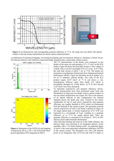
Figure 5. (a) Responsivity and corresponding quantum efficiency at 77 K. (b) Large area test diode with optical<br />
window in the top contact metalization <strong>for</strong> electro-optical characterization.<br />
a combination of mechanical lapping, wet-chemical polishing and wet-chemical etching to a thickness of about 20 µm.<br />
The detector hybrid is anti-reflection coated and finally integrated into a stand-alone camera system.<br />
The I-V characteristics of the diodes were measured on test<br />
diodes of the same size and geometry (37 x 37 µm 2 ) as the FPA<br />
diodes. Figure 4b shows the total dark current vs. bias voltage of<br />
a diode with a cut-off wavelength (5%) of 5.4 µm. At 0 V bias,<br />
the total dark current is below 1 pA at 77 K. The diodes are<br />
generation-recombination limited and show background-limited<br />
per<strong>for</strong>mance (BLIP). Figure 4a illustrates the R0A product of a<br />
set of 15 randomly selected diodes. The value of the R0A<br />
product equals 4x10 5 Ωcm 2 (a)<br />
at 77 K and shows a very<br />
homogeneous behavior apart from diode #15 which is<br />
presumably damaged by a bulk defect. At 67 K R0A beyond<br />
(b)<br />
Figure 6. Histogram of the NETD (a) and mapping<br />
of dead pixels (b) in a 256 x 256 <strong>InAs</strong>/Ga<strong>Sb</strong> <strong>short</strong><strong>period</strong><br />
superlattice FPA integrated on IDCA.<br />
1x10 6 Ωcm 2 have been measured.<br />
To determine responsivity and quantum efficiency electrooptical<br />
measurements have been per<strong>for</strong>med under front side<br />
illumination on large area test diodes with an optical window in<br />
the top contact metalization (see Figure 5b). Due to the absence<br />
of an optical reflector in this configuration, the infrared<br />
radiation passes the diode only once. Caused by the mirror<br />
metalization on top of each pixel, responsivity and quantum<br />
efficiency are roughly doubled in FPAs which are illuminated<br />
from the backside in the camera system. The spectrally resolved<br />
current responsivity of such a test diode is plotted in Figure 5a<br />
<strong>for</strong> single optical path. A current responsivity of 0.7 A/W was<br />
measured at a wavelength of 5 µm, resulting in a quantum<br />
efficiency of η = 17 % <strong>for</strong> single optical path. Thus, the<br />
quantum efficiency is estimated to be around η = 30 % in FPA<br />
detector pixels under backside illumination.<br />
After flip-chip bonding and removal of the Ga<strong>Sb</strong> substrate, the<br />
detector chips were mounted in an integrated detector cooler<br />
assembly with a 1 W linear Stirling cooler. An important figure<br />
of merit is the noise-equivalent temperature difference (NETD)<br />
of the camera system. The histogram over 256 x 256 detector<br />
pixels at an integration time of 6.5 ms and with F/2 optics is