InAs/(GaIn)Sb short-period superlattices for focal plane arrays
InAs/(GaIn)Sb short-period superlattices for focal plane arrays
InAs/(GaIn)Sb short-period superlattices for focal plane arrays

You also want an ePaper? Increase the reach of your titles
YUMPU automatically turns print PDFs into web optimized ePapers that Google loves.
(see Figure 1). The effective band gap EG of these structures can be adjusted from 0.3 eV to values below 0.1 eV by<br />
varying the thickness of the <strong>InAs</strong> layer or the indium mole fraction in the (GaxIn1-x)<strong>Sb</strong>. The growth is per<strong>for</strong>med by<br />
Molecular Beam Epitaxy (MBE) on 2” Ga<strong>Sb</strong> substrates which are commercially available with low defect densities.<br />
During growth, the strain can be kept sufficiently low by precisely controlling the interfaces between the <strong>InAs</strong> and the<br />
(<strong>GaIn</strong>)<strong>Sb</strong>. The MBE growth process offers promising prospects <strong>for</strong> future dual color / dual band sensors <strong>for</strong> 3 rd<br />
generation thermal imaging.<br />
For the realization of high per<strong>for</strong>mance IR-camera systems, Fraunhofer IAF cooperates with AIM Infrarot Module<br />
GmbH (AIM) located in Heilbronn, Germany. Fraunhofer IAF is committed to the development and fabrication of the<br />
detector chip, i.e., the MBE growth, process technology and electro-optical characterization. IAF’s fully processed<br />
detector chips are hybridized at AIM with a custom-designed silicon readout integrated circuit (ROIC) using flip-chip<br />
indium solder bump technology. These detector hybrids are mounted into a detector cooler assembly with a 1 W linear<br />
Stirling cooler, which is part of a complete IR imaging camera system. Subsequently, an overview of the Fraunhofer<br />
IAF / AIM superlattice technology will be presented.<br />
2. <strong>InAs</strong>/Ga<strong>Sb</strong> SHORT-PERIOD SUPERLATTICES FOR THE MID-IR SPECTRAL RANGE<br />
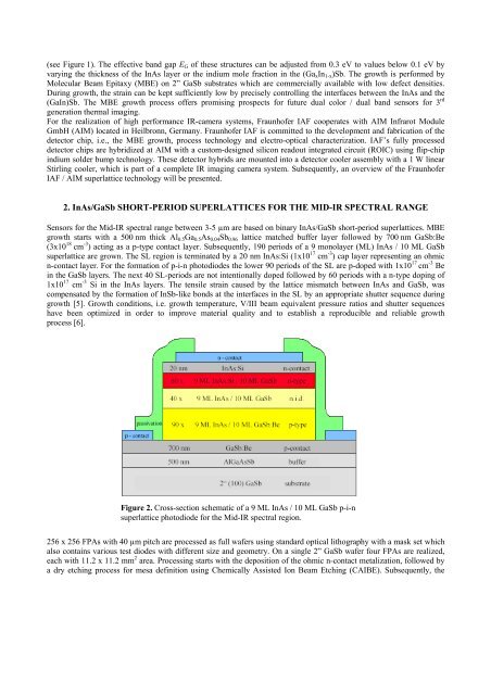
Sensors <strong>for</strong> the Mid-IR spectral range between 3-5 µm are based on binary <strong>InAs</strong>/Ga<strong>Sb</strong> <strong>short</strong>-<strong>period</strong> <strong>superlattices</strong>. MBE<br />
growth starts with a 500 nm thick Al0.5Ga0.5As0.04<strong>Sb</strong>0.96 lattice matched buffer layer followed by 700 nm Ga<strong>Sb</strong>:Be<br />
(3x10 18 cm -3 ) acting as a p-type contact layer. Subsequently, 190 <strong>period</strong>s of a 9 monolayer (ML) <strong>InAs</strong> / 10 ML Ga<strong>Sb</strong><br />
superlattice are grown. The SL region is terminated by a 20 nm <strong>InAs</strong>:Si (1x10 17 cm -3 ) cap layer representing an ohmic<br />
n-contact layer. For the <strong>for</strong>mation of p-i-n photodiodes the lower 90 <strong>period</strong>s of the SL are p-doped with 1x10 17 cm -3 Be<br />
in the Ga<strong>Sb</strong> layers. The next 40 SL-<strong>period</strong>s are not intentionally doped followed by 60 <strong>period</strong>s with a n-type doping of<br />
1x10 17 cm -3 Si in the <strong>InAs</strong> layers. The tensile strain caused by the lattice mismatch between <strong>InAs</strong> and Ga<strong>Sb</strong>, was<br />
compensated by the <strong>for</strong>mation of In<strong>Sb</strong>-like bonds at the interfaces in the SL by an appropriate shutter sequence during<br />
growth [5]. Growth conditions, i.e. growth temperature, V/III beam equivalent pressure ratios and shutter sequences<br />
have been optimized in order to improve material quality and to establish a reproducible and reliable growth<br />
process [6].<br />
Figure 2. Cross-section schematic of a 9 ML <strong>InAs</strong> / 10 ML Ga<strong>Sb</strong> p-i-n<br />
superlattice photodiode <strong>for</strong> the Mid-IR spectral region.<br />
256 x 256 FPAs with 40 µm pitch are processed as full wafers using standard optical lithography with a mask set which<br />
also contains various test diodes with different size and geometry. On a single 2” Ga<strong>Sb</strong> wafer four FPAs are realized,<br />
each with 11.2 x 11.2 mm 2 area. Processing starts with the deposition of the ohmic n-contact metalization, followed by<br />
a dry etching process <strong>for</strong> mesa definition using Chemically Assisted Ion Beam Etching (CAIBE). Subsequently, the