InAs/(GaIn)Sb short-period superlattices for focal plane arrays
InAs/(GaIn)Sb short-period superlattices for focal plane arrays
InAs/(GaIn)Sb short-period superlattices for focal plane arrays

Create successful ePaper yourself
Turn your PDF publications into a flip-book with our unique Google optimized e-Paper software.
Figure 9a shows a SEM image of mesas with 40 µm pitch in a 256x256 FPA arrangement after epitaxial overgrowth<br />
with the 150 nm thick Al0.5Ga0.5As0.04<strong>Sb</strong>0.96 layer. In Figure 9b the corner of such an FPA pixel is shown at higher<br />
magnification. The excellent surface morphology without polycrystalline phases is evident. In order to prevent<br />
oxidation of the Al-containing passivation layer, a 200 nm thick silicon nitride layer was deposited after removing the<br />
sample from the MBE system. Since the Fermi level at the p-n junction on the diode sidewall is defined by the<br />
Al0.5Ga0.5As0.04<strong>Sb</strong>0.96 layer, the electrical properties of the photodiode are not affected by this dielectric layer. The<br />
silicon nitride was used as an etch mask <strong>for</strong> wet chemical etching of the Al0.5Ga0.5As0.04<strong>Sb</strong>0.96 passivation and the Ga<strong>Sb</strong>cap<br />
layer. The wet chemical etchant chosen <strong>for</strong> this process step offers a sufficiently high selectivity to the Incontaining<br />
SL. Finally, ohmic n- and p-contact metalization layers were deposited.<br />
Various test diodes were wire-bonded after processing and characterized by dark I-V measurements. Since surface<br />
leakage currents occur at the mesa sidewalls, dark current measurements in dependence of the perimeter-to-area (P/A)<br />
ratio were carried out to separate the surface leakage currents from the bulk contributions. A convenient measure <strong>for</strong><br />
this investigation is the R0A product, since it is inversely proportional to the square of the limiting Johnson noise<br />
contribution [10].<br />
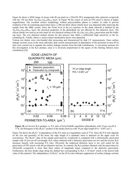
(R 0 A) -1 (Ω -1 cm -2 )<br />
10 3<br />
10 2<br />
10 1<br />
10 0<br />
10 -1<br />
10 -2<br />
EDGE LENGTH OF<br />
QUADRATIC MESA (µm)<br />
800 700 600 500 400 300200 200 100<br />
Dielectric passivation<br />
Passivation by overgrowth<br />
λ c = 10 µm<br />
(a) 77 K (b)<br />
77 K<br />
0.02 0.04 0.06<br />
PERIMETER-TO-AREA (µm -1 )<br />
70 µm edge length<br />
P/A = 0.057 µm -1<br />
10 3<br />
10 2<br />
10 1<br />
10 0<br />
10 -1<br />
0 2 4 6 8 10 12 10-2<br />
DIODE #<br />
Figure 10. (a) Inverse R0A product vs. P/A ratio of <strong>InAs</strong>/<strong>GaIn</strong><strong>Sb</strong> superlattice photodiodes with 10 µm cut-off at<br />
77 K. (b) Histogram of the (R0A) -1 product of the diodes from (a) with 70 µm edge length (P/A = 0.057 µm -1 ).<br />
Figure 10a shows the (R0A) -1 in dependence of the P/A ratio on a logarithmic scale at 77 K. Since the P/A ratio depends<br />
on the size and geometry of the mesa, the edge length of a quadratic mesa is depicted on the upper scale <strong>for</strong><br />
convenience. The (R0A) -1 data of the sample passivated by overgrowth is compared with a dielectrically passivated<br />
sample with 10 µm cut-off wavelength. R0A values obtained with a dielectric passivation are low and the inverse R0A<br />
increases linearly with increasing P/A ratio. Obviously the employed dielectric layer is not well suited <strong>for</strong> the<br />
passivation of FPA pixels with 40 µm diameter and less. In contrast, the R0A product obtained with the passivation by<br />
AlGaAs<strong>Sb</strong> overgrowth is more than three orders of magnitude larger compared to the dielectric passivation.<br />
Furthermore, the best diodes align along the dashed line corresponding to R0A ≈ 10 Ωcm 2 which is the known bulk<br />
value of this material. The independency of (R0A) -1 on the (P/A) ratio indicates suppression of surface leakage currents<br />
(R 0 A) -1 (Ω -1 cm -2 )