InAs/(GaIn)Sb short-period superlattices for focal plane arrays
InAs/(GaIn)Sb short-period superlattices for focal plane arrays
InAs/(GaIn)Sb short-period superlattices for focal plane arrays

You also want an ePaper? Increase the reach of your titles
YUMPU automatically turns print PDFs into web optimized ePapers that Google loves.
Figure 7. Thermal images of the first fully integrated 256 x 256 Mid-IR superlattice camera with 9.4 mK NETD.<br />
plotted in Figure 6a. Excellent spatial uni<strong>for</strong>mity is obtained over the array, resulting in a median NETD value of<br />
9.4 mK at a detector temperature of 73 K. For an integration time of 1.25 ms a NETD value of 25 mK has been<br />
measured.<br />
The very good homogeneity of the NETD across the entire 256 x 256 array is illustrated in Figure 6b which shows a<br />
mapping of defective pixels. In total, pixel outages are well below 1% and appear statistically distributed,<br />
predominantly as single pixel faults without large clusters.<br />
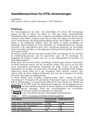
The excellent image quality delivered from the <strong>InAs</strong>/Ga<strong>Sb</strong> SL mid-IR camera system is shown in Figure 7. The fine<br />
structure of the clothing proves the good spatial resolution and the low cross talk between neighboring detector<br />
elements in the FPA. With this camera demonstrator, it is obvious, that <strong>InAs</strong>/Ga<strong>Sb</strong> SLs are in the position to provide<br />
low NETD values at <strong>short</strong> integration times comparable with HgCdTe detectors. The excellent per<strong>for</strong>mance of the<br />
camera system demonstrates the high potential of <strong>InAs</strong>/Ga<strong>Sb</strong> SLs <strong>for</strong> the fabrication of future IR imaging systems.<br />
3. <strong>InAs</strong>/<strong>GaIn</strong><strong>Sb</strong> SHORT-PERIOD SUPERLATTICES FOR 8-10 µm<br />
The main technological challenge <strong>for</strong> the fabrication of large <strong>for</strong>mat FPAs with pixel sizes of 40 µm and less is the<br />
occurrence of surface leakage currents. Since surface leakage currents in low band gap devices are mostly due to<br />
tunneling of electrons, these currents increase exponentially when the band gap of the device shifts to longer<br />
wavelengths. Besides efficient suppression of surface leakage currents, a passivation layer suitable <strong>for</strong> production<br />
purposes must withstand various treatments occurring during the subsequent processing and integration up to the<br />
camera level. There<strong>for</strong>e, ammonium-sulfide treatments, which have been investigated by several groups [7,8], seem<br />
difficult to be incorporated in a production process. Up to now the reproducibility and long-term stability achieved by<br />
the deposition of a dielectric passivation layer is not sufficient <strong>for</strong> photodiodes in the 8 – 12 µm range. There<strong>for</strong>e, we<br />
investigated the epitaxial overgrowth of <strong>InAs</strong>/(<strong>GaIn</strong>)<strong>Sb</strong> <strong>short</strong>-<strong>period</strong> superlattice mesa devices with lattice matched<br />
AlxGa1-xAsy<strong>Sb</strong>1-y by MBE [9].<br />
The approach is demonstrated using an <strong>InAs</strong>/(Ga0.75In0.25)<strong>Sb</strong> <strong>short</strong> <strong>period</strong> superlattice p-i-n photodiode with a cut-off<br />
wavelength around 10 µm at 77 K grown by MBE on undoped 2” (001)-Ga<strong>Sb</strong> substrate. MBE growth started with a<br />
500 nm thick Al0.5Ga0.5As0.04<strong>Sb</strong>0.96 lattice matched buffer layer followed by a p-type contact layer comprised of 700 nm<br />
Ga<strong>Sb</strong>:Be (3x10 18 cm -3 ). The active region contains 190 <strong>period</strong>s of an 8.6 ML <strong>InAs</strong> / 5.0 ML (Ga0.75In0.25)<strong>Sb</strong> superlattice<br />
structure. The active region is terminated by a 30 nm Ga<strong>Sb</strong> cap layer. The lower 90 <strong>period</strong>s of the SL were p-doped<br />
with 1x10 17 cm -3 Be in the Ga0.75In0.25<strong>Sb</strong> layers. The next 40 SL-<strong>period</strong>s were not intentionally doped followed by 60<br />
<strong>period</strong>s with an n-doping of 1x10 17 cm -3 Si in the <strong>InAs</strong> layers.