InAs/(GaIn)Sb short-period superlattices for focal plane arrays
InAs/(GaIn)Sb short-period superlattices for focal plane arrays
InAs/(GaIn)Sb short-period superlattices for focal plane arrays

You also want an ePaper? Increase the reach of your titles
YUMPU automatically turns print PDFs into web optimized ePapers that Google loves.
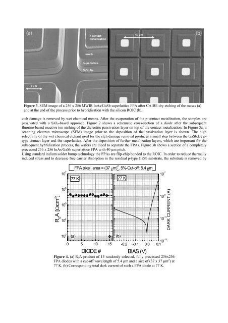
Figure 3. SEM image of a 256 x 256 MWIR <strong>InAs</strong>/Ga<strong>Sb</strong> superlattice FPA after CAIBE dry etching of the mesas (a)<br />
and at the end of the process prior to hybridization with the silicon ROIC (b).<br />
etch damage is removed by wet chemical means. After the evaporation of the p-contact metalization, the samples are<br />
passivated with a SiO2-based approach. Figure 2 shows a schematic cross-section of a diode after the subsequent<br />
fluorine-based reactive ion etching of the dielectric passivation layer on top of the contact metalization. In Figure 3a, a<br />
scanning electron microscope (SEM) image prior to the deposition of the passivation layer is shown. The high<br />
selectivity of the wet chemical etchant used <strong>for</strong> the etch damage removal produces a small step between the Ga<strong>Sb</strong>:Be ptype<br />
contact layer and the superlattice. After the deposition of further metalization layers, which are important <strong>for</strong> the<br />
subsequent hybridization process, the wafers are diced to separate the FPAs. Figure 3b shows a section of a completely<br />
processed 256 x 256 <strong>InAs</strong>/Ga<strong>Sb</strong> superlattice FPA with 40 µm pitch.<br />
Using standard indium solder bump technology the FPAs are flip-chip bonded to the ROIC. In order to reduce thermally<br />
induced stress and to decrease free carrier absorption in the residual p-type Ga<strong>Sb</strong> substrate, the substrate is removed by<br />
R 0 A [Ωcm 2 ]<br />
10 7<br />
10 6<br />
10 5<br />
10 4<br />
10 3<br />
FPA pixel, area = (37 µm) 2 , 5%-Cut-off: 5.4 µm<br />
77 K<br />
(a)<br />
0 5 10 15<br />
DIODE #<br />
77 K<br />
(b)<br />
10 -7<br />
10 -9<br />
10 -11<br />
-0.2 -0.1 0.0 0.1 10-13<br />
BIAS (V)<br />
Figure 4. (a) R0A product of 15 randomly selected, fully processed 256x256<br />
FPA diodes with a cut-off wavelength of 5.4 µm and a size of (37 x 37 µm 2 ) at<br />
77 K. (b) Corresponding total dark current of such a FPA diode at 77 K.<br />
DARK CURRENT (A)