InAs/(GaIn)Sb short-period superlattices for focal plane arrays
InAs/(GaIn)Sb short-period superlattices for focal plane arrays
InAs/(GaIn)Sb short-period superlattices for focal plane arrays

Create successful ePaper yourself
Turn your PDF publications into a flip-book with our unique Google optimized e-Paper software.
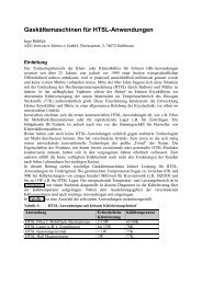
Figure 8. Cross-section schematic of a <strong>InAs</strong>/<strong>GaIn</strong><strong>Sb</strong> superlattice <strong>for</strong> the 8-12 µm spectral<br />
range passivated by MBE overgrowth with lattice matched Al0.5Ga0.5As0.04<strong>Sb</strong>0.96.<br />
A full wafer process using standard optical lithography with a mask set containing various test diodes of different size<br />
and geometry was used to process the wafer. A cross section scheme of a completely processed mesa detector is<br />
presented in Figure 8. The processing sequence starts with the mesa definition which was done wet-chemically using<br />
citric acid. In order to ensure homogeneous wet etching and overgrowth of both sidewalls of rectangular shaped mesas,<br />
the mesa mask was aligned at 45 degree to the natural cleavage <strong>plane</strong>s of the crystal. In this way two slightly positive<br />
facets <strong>for</strong> both the (100) and (010) oriented mesa sidewalls were achieved. After mesa etching, great care was taken to<br />
remove the resist completely. The sample was then re-inserted into the MBE chamber and the residual surface oxide<br />
was thermally desorbed. Subsequently, epitaxial overgrowth of the mesa-structured sample with a 150 m thick<br />
Al0.5Ga0.5As0.04<strong>Sb</strong>0.96 passivation layer was per<strong>for</strong>med. During oxide desorption and overgrowth group-V stabilization of<br />
the semiconductor surface was ensured by a sufficiently high <strong>Sb</strong>-flux.<br />
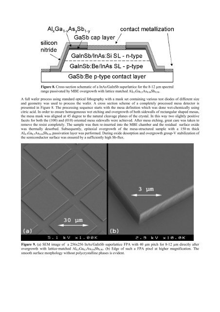
Figure 9. (a) SEM image of a 256x256 <strong>InAs</strong>/<strong>GaIn</strong><strong>Sb</strong> superlattice FPA with 40 µm pitch <strong>for</strong> 8-12 µm directly after<br />
overgrowth with lattice-matched Al0.5Ga0.5As0.04<strong>Sb</strong>0.96. (b) Edge of such a FPA pixel at higher magnification. The<br />
smooth surface morphology without polycrystalline phases is evident.