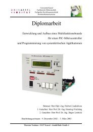
DSP Signal Generator Implementation On C6713 DSK - ComLab
DSP Signal Generator Implementation On C6713 DSK - ComLab
DSP Signal Generator Implementation On C6713 DSK - ComLab

Create successful ePaper yourself
Turn your PDF publications into a flip-book with our unique Google optimized e-Paper software.
<strong>DSP</strong> <strong>Signal</strong> <strong>Generator</strong> <strong>Implementation</strong><br />
<strong>On</strong> <strong>C6713</strong> <strong>DSK</strong><br />
Communications Laboratory – University of Kassel<br />
Project Work<br />
by<br />
Kamran Khan (28247463)<br />
Supervisor: Dipl.–Ing. Thomas Edlich
Declaration<br />
With this I declare that the present Project Report was made by myself. Prohibited means were not<br />
used and only the aids specified in the Project Report were applied. All parts which are taken over<br />
word-to-word or analogous from literature and other publications are quoted and identified.<br />
Kassel, December 9, 2009.<br />
Kamran Khan
Table of Contents<br />
Acknowledgements<br />
1 Introduction…...………………………………………………………………………………1<br />
1.1 Hardware and Software Tool……………………………………………………………....3<br />
1.2 <strong>Signal</strong> <strong>Generator</strong>…..…………….…………………………………………………………6<br />
1.2.1 Function <strong>Generator</strong>……………………………………………………………………..6<br />
1.2.2 Arbitrary Waveform <strong>Generator</strong>………………………………………………………...7<br />
1.2.3 Applied Fields for <strong>Signal</strong> <strong>Generator</strong>……………………………………………………8<br />
1.3 Project Motivation………………………………………………………………………….9<br />
2 Concept………………………………………………………………………………………10<br />
2.1 Waveform Generation……………………………………………………………………..10<br />
2.2 Pseudo Random Noise Sequence Generation……………………………………………..11<br />
2.3 Digital Modulation Schemes………………………………………………………………11<br />
3 <strong>Implementation</strong>…………………………………………………………………...…………12<br />
3.1 Waveform Generation…………………………………………………………………….12<br />
3.1.1 Sine Wave Generation………………………………………………………………...12<br />
3.1.2 Square Wave Generation……………………………………………………………...15<br />
3.1.3 Triangular Wave Generation………………………………………………………….16<br />
3.1.4 Sawtooth Wave Generation…………………………………………………………...19<br />
3.1.5 Multi-tone <strong>Signal</strong> Generation………………………………………………………....21<br />
3.2 Pseudo Random Noise Sequence Generation……………………………………………..22<br />
3.3 Digital Modulation Schemes……………………………………………………………….26<br />
3.3.1 Pulse Amplitude Modulation………………………………………………………….26<br />
3.3.1.1 4- Level Pulse Amplitude Modulation………………………………………...27<br />
3.3.1.2 8- Level Pulse Amplitude Modulation………………………………………...29<br />
3.2.2 Phase Shift Keying…………………………………………………………………….31<br />
3.3.2.1 Binary Phase Shift Keying……………………………………………………..31<br />
3.3.2.2 Quadrature Phase Shift Keying………………………………………………...34<br />
4 Conclusion and Future Work……………………………………………………………….37<br />
Appendix………………………………………………………………………………………...38<br />
<strong>Signal</strong> <strong>Generator</strong> Menu…………………………………………………………………………..38<br />
References……………………………………………………………………………………….40
Acknowledgments<br />
All that I have achieved during my time as a student at the Communications Laboratory would<br />
not have been possible without the support of Prof. Dr. sc. techn. Dirk Dahlhaus, Head of<br />
Communications Laboratory, who has always shown resolute faith in me. Respectful mention<br />
must also be made of Dipl.-Ing. Herbert Lindenborn for his invaluable guidance whenever I<br />
sought an audience with him.<br />
If not for the thoughtful insight and sharp acumen of my project advisor Dipl.-Ing. Thomas<br />
Edlich, this project would perhaps not have seen the light of the day; I thank him for bearing<br />
with my idiosyncrasies and leading me back to the right path whenever I wandered off-course<br />
during my project, but most of all I thank him for taking time out of his busy schedule for me<br />
and enlightening me with his invaluable suggestions. Working with him has been a great<br />
learning experience. His motivation to work and professionalism has inspired me a lot.<br />
I am grateful to my friends specially Ibrahim and Zemene for their constructive criticism and<br />
suggestions. Last but not least, I would like to thank my family for always being there for me<br />
through the ups and downs of life.
1 Introduction<br />
Mostly sensors generate analog signals in response to various phenomena. <strong>Signal</strong> processing can<br />
be carried out either in analog or digital domain. To do processing of analog signals in digital<br />
domain, first digital signal is obtained by sampling and followed by quantization (digitization).<br />
The digitization can be obtained by analog to digital converter (ADC).<br />
The role of digital signal processor (<strong>DSP</strong>) is the manipulation of digital signals so as to extract<br />
desired information. In order to interface <strong>DSP</strong> with analog world, digital to analog converters<br />
(DAC) are used. Figure below shows basic components of a <strong>DSP</strong> system [1].<br />
Figure 1.1: Main components of a <strong>DSP</strong> system [1]<br />
ADC captures and inputs the signal. The resulting digital representation of the input signal is<br />
processed by <strong>DSP</strong> such as C6x and then output through DAC. Within in the basic <strong>DSP</strong> system,<br />
anti aliasing filter at input to remove erroneous signals and output filter to smooth the processed<br />
data is also used [2].<br />
There are various reasons to process the analog signals in the digital domain:<br />
• The same <strong>DSP</strong> hardware can be used for various applications by just changing the code.<br />
• Digital circuits are more stable and tolerant than analog circuits.<br />
• Many filters and adaptive systems are realizable only by the digital manipulation of<br />
signals.<br />
1
Digital signal processing can be carried out on various platforms such as customized very large<br />
scale integrated (VLSI) circuits and <strong>DSP</strong>. A comparative review of both the platforms is as<br />
follows:<br />
• <strong>DSP</strong>s are programmable allowing fair amount of application flexibility which not the<br />
case with hardwired digital circuits.<br />
• <strong>DSP</strong>s are cost effective due to mass production and can be used for various applications<br />
whereas VLSI chip is normally built for a signal application.<br />
• Often quite high sampling rates can be obtained by customized chips where in <strong>DSP</strong><br />
sampling rates are limited due to architecture design and peripheral constraints [1].<br />
Large market shares of <strong>DSP</strong>s belong to cost-effective real time embedded systems such as cell<br />
phones and modems. Real time requires keeping processing pace with some external event [2] or<br />
in other words completing the processing within the available time between samples which of<br />
course depends upon application. Real time processing depends upon two aspects a) sampling<br />
rate b) system latencies (delays) [1].<br />
Figure 1.2: Maximum number of instructions to meet real time =<br />
Time between samples/ Instruction cycle time [1]<br />
2
1.1 Hardware and Software Tools<br />
Many Companies produce <strong>DSP</strong>s such as Motorola, NEC, SGS-Thompson, Conexant, Lucent<br />
Technologies and Texas Instruments (TI). In this project, <strong>DSP</strong> TMS320<strong>C6713</strong> manufactured and<br />
designed by TI is used. <strong>DSP</strong>s such as TMS320C6x are special purpose microprocessors by TI<br />
with specialized architecture which is well suited for numerical intensive calculations. <strong>DSP</strong>s<br />
offer wide range of applications from image processing to communications such as cellular<br />
phones, printers, digital cameras MP3 players and so on [2][8].<br />
The TMS320<strong>C6713</strong> <strong>DSP</strong> is very powerful by itself, but for development of programs, a<br />
supporting architecture is required to store programs and data and to bring signals on and off the<br />
board. In order to use <strong>DSP</strong> a circuit board is provided that contains appropriate components.<br />
Together, Code Composer Studio (CCS), <strong>DSP</strong> chip, and supporting hardware make up the <strong>DSP</strong><br />
starter kit (<strong>DSK</strong>) [8]. Figure below shows the <strong>C6713</strong> <strong>DSK</strong> board.<br />
Figure 1.3: <strong>C6713</strong> <strong>DSK</strong> Board [1]<br />
3
The 6713 <strong>DSK</strong> board includes following hardware:<br />
• <strong>C6713</strong> <strong>DSP</strong> operating at 225 MHz<br />
• 4 Kbytes memory for L1D data cache<br />
• 4 Kbytes memory for L1P program cache<br />
• 256 Kbytes memory for L2 memory<br />
• 8 Mbytes of onboard SDRAM (Synchronous Dynamic RAM)<br />
• 512 Kbytes of flash memory<br />
• 16-bit stereo codec AIC23 with sampling frequency of 8 KHz to 96 KHz<br />
CCS software tool is used to generate TMS320C6x executable files. CCS includes the assembler,<br />
linker, compiler, and simulator and debugger utilities. Figure 1.4 shows the intermediate steps<br />
involved for going from a source file to an executable file. In the absence of target board the<br />
simulator can be used to verify the code functionality, however in the absence of simulator,<br />
Interrupt Service Routine (ISR) cannot to be used to read signals samples from a signal source.<br />
To be able to process signal in real time <strong>DSK</strong> or an Evaluation Module (EVM) is required for<br />
code development. Other testing equipments include function generator, oscilloscope,<br />
microphone and cable with audio jacks. A <strong>DSK</strong> board can be connected through PC host through<br />
parallel or USB port. Two standard audio jacks are used for signal interfacing with <strong>DSK</strong> board<br />
[1] [3].<br />
Figure 1.4: C6x CCS Software Tool [1]<br />
4
All the necessary files and steps required to build a project on code composer studio are<br />
explained in detail in [4]. Assuming CCS is installed in C drive, below is a summarized listing of<br />
steps and files required to make a project:<br />
• Open CCS.<br />
• To create new project go to Project→ New. Remember to select target TMS320C67XX.<br />
• Go to Debug and select Connect. Now the target board is connected to CCS.<br />
• Add source file (.c) to the project.<br />
• From the support folder (included in the CD) add the files c6713dskinit.c, <strong>C6713</strong>dsk.cmd<br />
and vectors_poll.asm to the project. It is important to note that if program is interrupt<br />
based then vectors_poll.asm should be replaced by vectors_intr.asm.<br />
• Add run-time support library file rts6700.lib, board support library file dsk6713bsl.lib<br />
and chip support library file csl6713.lib to the project. These files can be found in<br />
C:\<strong>C6713</strong>\C6000 under subdirectories cgtools\lib, dsk6713\lib and csl\lib respectively.<br />
• Go to Project→Build options. Select Compiler tab and go to Basic in Category listing.<br />
Change the Target Version to C671x(-mv6710) now select Advanced in the Category<br />
listing and change the Memory Models to --mem_model:data=far and in the last go to<br />
Preprocessor in the Category listing and change the Pre-Define Symbol and Include<br />
Search Path to CHIP_6713 and C:\<strong>C6713</strong>\C6000\dsk6713\include respectively.<br />
• Go to Project → Rebuild All.<br />
• File → Load Program.<br />
• Debug → Run<br />
5
1.2 <strong>Signal</strong> <strong>Generator</strong><br />
The signal generator is referred to a wide range of devices used to test electronic equipments by<br />
generating a signal whose frequency, wave shape, and amplitude are independently adjustable<br />
over a wide range of settings [9].<br />
<strong>Signal</strong> generator come in many different forms. The most prevalent signal generator types<br />
include function generator and arbitrary waveform generator. The signal generator types vary in<br />
their feature and functionality (and at varying level of expense) and are suitable for many<br />
different applications; in general, no single device is suitable for all possible applications [10].<br />
1.2.1 Function <strong>Generator</strong><br />
Function generators create built-in waveforms, such as sine, square or triangle waves, at<br />
adjustable frequencies and amplitude. Some function generators can also generate white or pink<br />
noise.<br />
Function generators can be either analog or digital based. Analog based function generators use<br />
electrical circuit which is combination of capacitor, resistor, inductors and other hardware to<br />
create simple functions and often they are used when a static sine or square wave at a specified<br />
frequency is required in a certain application.<br />
Digital based function generators use combination of <strong>DSP</strong>, DAC and memory buffer to<br />
dynamically create signals. Many signal generators create signals by dividing an internal<br />
timebase by an integer factor. This is called the divide-by-N method. Divide-by-N clocking,<br />
however, gives a limited set of frequencies. Figure 1.5 shows a basic architecture of digital based<br />
function generators.<br />
6
Figure 1.5: Digital based Function <strong>Generator</strong> [10]<br />
Typically one complete cycle of the waveform which is to be generated is stored in the memory<br />
lookup table. The phase accumulator keeps track of the current phase of the output function. To<br />
output a very low frequency, the phase difference between the samples should be small. For<br />
example, a low frequency sine may have a phase difference of 1 degree such that sample 0 of<br />
the waveform would be the amplitude of the sine wave at 0 degrees; sample 1 of the waveform<br />
would be the amplitude of the sine wave at 1 degree, and so on. All 360degrees of the sinusoid,<br />
or exactly one cycle, would be output after 360 samples. A higher frequency sine wave may have<br />
a phase difference of 10 degrees or more. For phase difference between samples equal to 10<br />
degree, one cycle of a sine wave would be generated in 36 samples. With a fixed sampling<br />
frequency, the low frequency sine wave would be 10 times lower in frequency than the high<br />
frequency sine wave [10].<br />
1.2.2 Arbitrary Waveform <strong>Generator</strong>s (AWG)<br />
Arbitrary Waveform <strong>Generator</strong>s (AWG), are sophisticated signal generators which allow the user<br />
to generate arbitrary waveforms, within certain limits of frequency range, accuracy, and output<br />
level.<br />
7
Unlike function generators, which are limited to a simple set of waveforms; AWGs are much<br />
more flexible. AWGs are generally more expensive than function generators, and are often more<br />
highly limited in available bandwidth; as a result, they are generally limited to higher end design<br />
and test applications [11].<br />
Figure 1.6: Arbitrary Waveform <strong>Generator</strong> [12]<br />
AWGs can also operate as conventional function generators. Mostly they include standard<br />
waveforms such as sine, square, ramp, triangle, and noise. Some units include additional built in<br />
waveforms such as sinx/x, cardiac waveform while other may display a graph of the waveform<br />
on their screen. Some AWGs allow multiple channels to be operated with precisely controlled<br />
phase offsets or ratio-related frequencies. This allows the generation of polyphase sine waves<br />
and IQ constellations. Complex channel modulations are also possible [12].<br />
1.2.3 Applied Fields for <strong>Signal</strong> <strong>Generator</strong><br />
The generation of signals is an important development in the troubleshooting and development<br />
of electronic design. The signal generator is used to provide known test conditions for the<br />
performance evaluation of electronic system design and for replacing signals that are missing in<br />
system during repairing work. While signal generators are widely used to test and maintain a<br />
wide range of RF equipment, such as radio receivers and transmitters, they are also extremely<br />
useful for testing digital, clock driven systems, especially high speed serial storage and serial<br />
communication ICs, circuit boards and devices. In general signal generators are used in<br />
8
designing, testing, troubleshooting, and repairing electronic devices specially related to<br />
communication. Few of the examples in which signal generator can be used are:<br />
• Testing setup for ICs and circuit boards for digital or differential output plus frequency<br />
sweep<br />
• Testing the IF and RF sections of receivers and mobile communication bands<br />
• Testing amplifiers for gain and for the 1 dB compression point<br />
• Using as a programmable clock generator<br />
• Calibrate receivers<br />
• Low frequency filter testing (down to 1 Hz)<br />
• Local oscillator source<br />
• Radio frequency (RF) Exciter<br />
Audio signal generators produce signals in a range from a few Hz up to several kHz. <strong>Signal</strong>s can<br />
be injected into audio amplifiers to see how they behave at various audio frequencies.<br />
Amplification and frequency response can be measured and distortion of the signal can be<br />
observed. RF generators can provide frequencies from about 100 kHz up to several hundred<br />
MHz. With radio frequency generators it is usually possible to modulate the RF with an audio<br />
signal to simulate a radio station. Amplitude and frequency modulation are available. Using an<br />
RF generator the various tuned circuits in a radio can be adjusted for peak performance [13] [14].<br />
1.3 Project Motivation<br />
Due to various uses of signal generator in different fields of application, there is always a need of<br />
creating a customized signal generator which could suffice the needs in different scenarios. The<br />
basic task of this project is to create <strong>C6713</strong> <strong>DSK</strong> implementation of specialized signal generator<br />
which could mimic the functionality of various signal generators.<br />
9
2 Concept<br />
The task at hand is to program a signal generator using <strong>C6713</strong> <strong>DSK</strong> using its audio interfaces<br />
which could have various functionalities ranging from generating different waveforms to various<br />
digital modulation schemes. As compared to market available signal generators, implementation<br />
of signal generator on <strong>C6713</strong> <strong>DSK</strong> gives the user an added advantage that the functionalities of<br />
signal generator are not limited to predefined waveforms/options but different new features can<br />
be added in already present signal generator as desired by modifying the source code.<br />
Different features of the concept signal generator can be grouped as:<br />
• Waveform Generation<br />
• Pseudo Random Noise Sequence Generation<br />
• Digital Modulation Schemes<br />
A user can select any of the above stated categories by using the slider named “Mode” which is<br />
implemented in CCS using General Extension Language (GEL). GEL is an interpretive language<br />
similar to C which allows changing variable such as gain, sliding through different values while<br />
processor is still running [2].<br />
Now different options available to a user in each category are discussed below:<br />
2.1 Waveform Generation<br />
A user can select different waveforms such as sine wave, square wave, triangular wave, ramp<br />
(saw tooth) or multi tone signal using the “Mode” slider. Gain and frequency of sine wave,<br />
square wave, triangular wave and sawtooth wave can be altered using “Gain” and “Frequency”<br />
slider.<br />
In multi tone signal there are 4 sliders available to a user to change different attributes of multi<br />
tone signal. It is important to note that throughout the project where ever multi tone signal is<br />
referred, it is assumed to be consisting of only two tones.<br />
A “Gain” slider defines the overall gain of multi tone signal. The gain selected by “Gain” slider<br />
is distributed among two frequencies. These two frequencies can be selected independent of each<br />
10
other using slider “f1” and “f2”. Slider “Ratio_gain_f1_VS_f2” decides the ratio by which the<br />
overall gain is distributed among the two frequencies (f1 and f2) selected by slider “f1” and “f2”.<br />
2.2 Pseudo Random Noise Sequence Generation<br />
In this category a user can generate pseudo random noise sequence or can investigate the effect<br />
of noise on an external input signal. In both of these cases the “Gain” slider can be used to select<br />
appropriate gain of the noise as desired.<br />
2.3 Digital Modulation Schemes<br />
Different modulation schemes can be selected by the user using “mode” slider such as Pulse<br />
Amplitude Modulation (PAM) or Phase Shift Keying (PSK). The user has also the freedom to<br />
choose the modulation schemes, either to work either using Input signal from some external<br />
source or using predefined input signal for demonstration. Different variants of PAM and PSK<br />
modulations implemented in the concept signal generator are 4-level PAM, 8-level PAM, BPSK<br />
(Binary PSK) and QPSK (Quadrature PSK).<br />
11
3 <strong>Implementation</strong><br />
In this section implementation of signal generator on <strong>C6713</strong> <strong>DSK</strong> is discussed. For the ease of<br />
reader different functionalities of signal generator are discussed as independent modules where<br />
later all these modules are incorporated in a single program. To access the source code of this<br />
program, please refer to the file “sine_varFreq.c” which is present in the folder “sine_varFreq”,<br />
included in the attached CD-ROM. It is assumed that the reader has a basic knowledge of C/C++<br />
and has read [4].<br />
3.1 Waveform Generation<br />
The <strong>C6713</strong> <strong>DSK</strong> can be used to generate various types of waveforms which have wide range of<br />
applications in communication systems. In this section generation of periodic waveforms namely<br />
sine wave, square wave, triangular wave, sawtooth wave and multi tone signal generation is<br />
discussed.<br />
3.1.1 Sine Wave Generation<br />
<strong>On</strong>e of the main things to take in account in generating any waveform is writing the sample<br />
values of waveform on the codec at every sampling instant. In the DAC done at the codec these<br />
sample values of the waveform are first oversampled (to smoothen the waveform) and are then<br />
fed to a reconstruction filter (to cut frequencies out of band of interest).<br />
There are two techniques for sending the data to codec namely polling technique and interrupt<br />
technique. Polling technique uses a continuous procedure of testing when the data is ready.<br />
Although it is simpler technique than interrupt technique, it is less efficient since the input and<br />
output data needs to be continuously tested to determine when they are ready to be received or<br />
transmitted. Figure 3.1 shows sine wave generated using interrupts technique, source code is<br />
shown in figure 3.2.<br />
12
Figure 3.1: Sine Wave obtained with the Scope<br />
Line 3 in the code sets the sampling frequency to 96 KHz. Different sampling frequencies<br />
supported by AIC23 codec are 8, 16, 24, 32, 44.1, 48, and 96 kHz. Line 7 initializes a array<br />
sine_table of length 128 which will be later used as a buffer to store different sine values. Within<br />
the main function, line 19-21 generates the data for sine wave. When the program execution<br />
reaches the line 23, program execution halts and it starts listening for the interrupt which occur at<br />
every sampling period Ts. At each Interrupt, program execution goes to the interrupt service<br />
routine defined in the lines 9-14. Within the service routine, the value in the buffer sine_table<br />
indexed by the variable loop is written on to the codec. Then the index loop is incremented by an<br />
amount equal to frequency. After reaching the line 13, program execution goes back to line 23<br />
and then again starts listening for next interrupt and this process goes on. Variables gain and<br />
frequency defined in line 5 and 6 respectively set the gain and frequency of the generated sine<br />
wave.<br />
13
1 include "dsk6713_aic23.h" //support file for codec, <strong>DSK</strong><br />
2 #define sineTableLen 128<br />
3 Uint32 fs=<strong>DSK</strong>6713_AIC23_FREQ_96KHZ; //set sampling rate<br />
4 short loop = 0; //table index<br />
5 short gain =1;<br />
6 short frequency = 1;<br />
7 short sine_table[sineTableLen]={0}; // table initialization<br />
8 interrupt void c_int11() //interrupt service routine<br />
9 {<br />
10 output_sample(sine_table[loop]*gain); //output sine values<br />
11 loop += frequency; //increment frequency index<br />
12 loop = loop%sineTableLen; //reinitialize table if exceeds limit<br />
13 return; //return from interrupt<br />
14 } // end of interrpt routine<br />
15 void main()<br />
{<br />
16 short i=0;<br />
17 float pi=3.14159;<br />
18 for(i = 0; i < sineTableLen; i++)<br />
19 {<br />
20 sine_table[i] = 300*sin(2.0*pi*i/sineTableLen);<br />
21 }<br />
22 comm_intr(); //init <strong>DSK</strong>, codec, McBSP<br />
23 while(1); //infinite loop<br />
}<br />
Figure 3.2: Source code for sine wave generation<br />
These variables (gain and frequency) are controlled by the user during the program execution on<br />
<strong>DSP</strong> with the help of graphical user interface named “slider” as shown in the figure 3.3.<br />
Figure 3.3: Slider representing Amplitude of sine wave<br />
In the project we have set the Gain slider to take any discrete value from 1 to 100 determined by<br />
the user, correspondingly the gain variable can also take same range of values. In line 10 this<br />
gain variable is multiplied by different sine values to create a output sine wave of the same gain<br />
factor. Similarly we have set Frequency slider to take any discrete value from 1 to 20 determined<br />
14
y the user, correspondingly the frequency variable can also take same range of values.<br />
Subsequently for 20 different values taken by the frequency slider, we can have 20 different<br />
frequencies ranging from 750 Hz (approx) to 15 kHz (approx) with the step size of 750 Hz<br />
(approx).<br />
3.1.2 Square Wave Generation<br />
In this section square wave generation is discussed. In the line 7, figure 3.5, data buffer for<br />
containing square wave values is declared. In the main function, first half of the buffer<br />
square_table is filled up with value 300 while the second half of the buffer is filled up with value<br />
-300.<br />
Figure 3.4: Square Wave obtained with the Scope<br />
The maximum output signal which can be obtained with AIC23 codec present in 6713 <strong>DSK</strong> is<br />
6Vp-p. Correspondingly the maximum value which can be fed to the codec to produce distortion<br />
free output signal ranges from -2 15 to 2 15 -1 or between -32,768 and 32,767. In the lines 20 and 24<br />
square wave is initialized with 300 and -300 such that when square wave values are multiplied<br />
with the gain and sent to the output (line 10), for the maximum value of gain i.e. 100, the product<br />
of gain and square wave values lies with the allowed input range of the codec.<br />
15
1 include "dsk6713_aic23.h" //support file for codec, <strong>DSK</strong><br />
2 #define squareTableLen 800<br />
3 Uint32 fs=<strong>DSK</strong>6713_AIC23_FREQ_96KHZ; //set sampling rate<br />
4 short loop = 0; //table index<br />
5 short gain =1;<br />
6 short frequency = 1;<br />
7 short square_table[squareTableLen]={0}; // table initialization<br />
8 interrupt void c_int11() //interrupt service routine<br />
9 {<br />
10 output_sample(square_table[loop]*gain); //output square values<br />
11 loop += frequency; //increment frequency index<br />
12 loop = loop%squareTableLen; //reinitialize table if exceeds limit<br />
13 return; //return from interrupt<br />
14 } // end of interrpt routine<br />
15 void main()<br />
16 {<br />
17 short i=0;<br />
18 for(i=0; i < squareTableLen/2; i++)<br />
19 {<br />
20 square_table[i] = 300; // lookup table first half of waveform<br />
21 }<br />
22 for(i=squareTableLen/2; i < squareTableLen; i++)<br />
23 {<br />
24 square_table[i] = -300; // lookup table 2nd half of waveform<br />
25 }<br />
26 comm_intr(); //init <strong>DSK</strong>, codec, McBSP<br />
27 while(1); //infinite loop<br />
Figure 3.5: Source code for square wave generation<br />
3.1.3 Triangular Wave Generation<br />
Now we will discuss generation of triangular waves.<br />
Figure 3.6: Triangular Wave obtained with the Scope<br />
16
In the main function, buffer of values of triangular wave is defined in such a way that first entry<br />
in the buffer is given the value -300 (-0x12C) and as the index of the buffer increases the values<br />
in the buffer linearly decrease with the step defined in the line 18. When the index of the buffer<br />
reach in the middle of the buffer, then the values in the buffer again starts to increase linearly<br />
with the step size till it reaches the end of the buffer.<br />
1 include "dsk6713_aic23.h" //support file for codec, <strong>DSK</strong><br />
2 #define triangleTableLen 128<br />
3 Uint32 fs=<strong>DSK</strong>6713_AIC23_FREQ_96KHZ; //set sampling rate<br />
4 short loop = 0; //table index<br />
5 short gain =1;<br />
6 short frequency = 1;<br />
7 short triangle_table[triangleTableLen]={0}; // table initialization<br />
8 interrupt void c_int11() //interrupt service routine<br />
9 {<br />
10 output_sample(triangle_table[loop]*gain); //output triangle values<br />
11 loop += frequency; //increment frequency<br />
index<br />
12 loop = loop%triangleTableLen; //reinitialize if exceeds limit<br />
13 return; //return from interrupt<br />
14 } // end of interrpt routine<br />
15 void main()<br />
16 {<br />
17 short i=0;<br />
18 short step = 2 * 0x12C/ (triangleTableLen);<br />
19 for(i=0; i < triangleTableLen/2; i++)<br />
20 {<br />
21 triangle_table[i] = -0x12C + i * step; // First half of waveform<br />
22 }<br />
23 for(i=triangleTableLen/2; i < triangleTableLen; i++)<br />
24 {<br />
25 triangle_table[i] = triangle_table[i-1] - step; // second half of<br />
waveform<br />
26 }<br />
27 comm_intr(); //init <strong>DSK</strong>, codec, McBSP<br />
i //i i i<br />
Figure 3.7: Source code for triangular wave generation<br />
Another feature which can be easily incorporated with our current signal generator model is to<br />
control (ON/OFF) the generation of output (waveform/Noise/Digital Modulation schemes) with<br />
the help of DIP switch. As an example, figure 3.8 shows the sample code for controlling the<br />
generation of triangular wave with the help of DIP switch.<br />
17
In the main function, line 34 initializes the <strong>DSK</strong>, the AIC23 onboard <strong>DSK</strong> codec and two Multi<br />
channel Buffered Serial Ports (McBSP) on the <strong>C6713</strong> processor. The function comm_intr is<br />
present in communication and initialization support file c6713dskinit.c.Within c6713dskinit.c,<br />
the function <strong>DSK</strong>6713_init initializes the BSL file, which must be called before the two<br />
subsequent BSL functions <strong>DSK</strong>6713_LED_init and <strong>DSK</strong>6713_DIP_init (line 35 and 36), are<br />
invoked that initialize the four LEDs and the four DIP switches. In the line 11, the if statement<br />
becomes true when dip switch #0 is pressed and consequently LED #0 turns on (line 13) and<br />
waveform is generated (line 14).<br />
1 include "dsk6713_aic23.h" //support file for codec, <strong>DSK</strong><br />
2 #define triangleTableLen 128<br />
3 Uint32 fs=<strong>DSK</strong>6713_AIC23_FREQ_96KHZ; //set sampling rate<br />
4 short loop = 0; //table index<br />
5 short gain =1;<br />
6 short frequency = 1;<br />
7 short triangle_table[triangleTableLen]={0}; // table initialization<br />
8<br />
9 interrupt void c_int11() //interrupt service routine<br />
10 {<br />
11 if(<strong>DSK</strong>6713_DIP_get(0)==0) //=0 if switch #0 pressed<br />
12 {<br />
13 <strong>DSK</strong>6713_LED_on(0); //turn LED #0 ON<br />
14 output_sample(triangle_table[loop]*gain);//output triangle values<br />
15 loop += frequency; //increment frequency index<br />
16 loop = loop%triangleTableLen; //reinitialize if exceeds limit<br />
17 }<br />
18 else <strong>DSK</strong>6713_LED_off(0); //LED #0 off<br />
19 return; //return from interrupt<br />
20 }<br />
21<br />
22 void main()<br />
23 {<br />
24 short i=0;<br />
25 short step = 2 * 0x12C/ (triangleTableLen);<br />
26 for(i=0; i < triangleTableLen/2; i++)<br />
27 {<br />
28 triangle_table[i] = -0x12C + i * step; // First half of waveform<br />
29 }<br />
30 for(i=triangleTableLen/2; i < triangleTableLen; i++)<br />
31 {<br />
32 triangle_table[i] = triangle_table[i-1] - step; // second half<br />
33 }<br />
34 comm_intr(); //init <strong>DSK</strong>, codec, McBSP<br />
35 <strong>DSK</strong>6713_LED_init(); //init LED from BSL<br />
36 <strong>DSK</strong>6713_DIP_init(); //init DIP from BSL<br />
37 while(1); //infinite loop<br />
38 } //end of main<br />
Figure 3.8: Source code for controlling triangular wave through DIP switch<br />
18
3.1.4 Sawtooth Wave (Ramp) Generation<br />
Now we will discuss the generation of sawtooth wave. Sawtooth wave is also sometimes referred<br />
as ramp.<br />
Figure 3.9: Sawtooth Wave obtained with the Scope<br />
Ramp is created (Figure 3.10) in approximately the same way as the triangular wave with only<br />
the difference that after buffer index has reached the middle of buffer (line 22) unlike, triangular<br />
wave, values in the buffer ramp_table continue to decrease linearly with the step defined in line<br />
19 until it reaches the end of the buffer. Here, it is important to note that at the output we get –ve<br />
sloped ramp due to the 2’s- complement format of the AIC23 codec [2].<br />
Another functionality which we can easily include in our current signal generator is to output<br />
ramp with positive and negative slope on left and right channel at the same time. Figure 3.11<br />
shows the corresponding program listing. This program is same as in figure 3.10 except some<br />
changes in the ISR, so only ISR is shown in the figure 3.11. In line 6, a structure AIC23_data is<br />
declared which could hold data of two channels. This program uses the same data buffer<br />
ramp_table to create both +ve sloped and –ve sloped ramp. For the –ve sloped ramp at the output<br />
(left channel), the loop index starts from the start of ramp_table while for +ve sloped ramp at the<br />
output (right channel), the loop index starts from the end of ramp_table and then gradually<br />
decrease with the step defined by the frequency.<br />
19
1 include "dsk6713_aic23.h" //support file for codec, <strong>DSK</strong><br />
2 #define rampTableLen 128<br />
3 Uint32 fs=<strong>DSK</strong>6713_AIC23_FREQ_96KHZ; //set sampling rate<br />
4 short loop = 0; //table index<br />
5 short gain =1;<br />
6 short frequency = 1;<br />
7 short ramp_table[rampTableLen]={0}; // table initialization<br />
8 interrupt void c_int11() //interrupt service routine<br />
9 {<br />
10 output_sample(ramp_table[loop]*gain); //output ramp values<br />
11 loop += frequency; //increment frequency index<br />
12 loop = loop%rampTableLen; //reinitialize if exceeds beyond limit<br />
13 return;<br />
14 } // end of interrpt routine<br />
15 void main()<br />
16 {<br />
17 short i=0;<br />
18 short step2 = 2*0x12C/ (rampTableLen);<br />
19 for(i=0; i < rampTableLen; i++) // Fill the lookup table<br />
20 {<br />
21 ramp_table[i] = -0x12C + i * step2;<br />
22 }<br />
23 comm_intr(); //init <strong>DSK</strong>, codec, McBSP<br />
24 while(1); //infinite loop<br />
}<br />
Figure 3.10: Source code for sawtooth wave generation<br />
1 short loop1 = 0; //table index<br />
2 short loop2 = rampTableLen-1; //table index<br />
3 short gain =1;<br />
4 short frequency = 1;<br />
5 short ramp_table[rampTableLen]={0}; // table initialization<br />
6 union {Uint32 combo; short channel[2];} AIC23_data;<br />
7<br />
8 interrupt void c_int11() //interrupt service routine<br />
9 {<br />
10 AIC23_data.channel[LEFT]=ramp_table[loop1]*gain; //output ramp values<br />
11 loop1 += frequency; //increment frequency index<br />
12 loop1 = loop1%rampTableLen; //reinitialize if exceeds beyond limit<br />
13<br />
14 AIC23_data.channel[RIGHT]=ramp_table[loop2]*gain; //output ramp values<br />
15 loop2 -= frequency; //increment frequency index<br />
16 if (loop2
3.1.5 Multi-tone <strong>Signal</strong> Generation<br />
Multi-tone signal generation uses the same method to generate the buffer for storing the values<br />
of the sine wave as depicted in the figure 3.2 with only the difference in the ISR. Figure 3.13<br />
show the interrupt service routine for generating Multi-tone signal.<br />
Figure 3.12: Multi-tone wave obtained with the Scope<br />
In the line 12 two sinusoidal signals are generated and added together to form a multi-tone<br />
signal. The frequencies of these signals are determined by the variable f1 and f2 which are<br />
controlled through the slider. Variable gain defines the overall gain of the multi-tone signal<br />
which is distributed among the two sinusoids by the proportion determined by the variable ratio.<br />
The ratio is also user adjustable through the slider created with the help of GEL.<br />
1 include "dsk6713_aic23.h" //support file for codec, <strong>DSK</strong><br />
2 #define sineTableLen 128<br />
3 Uint32 fs=<strong>DSK</strong>6713_AIC23_FREQ_96KHZ; //set sampling rate<br />
4 short gain = 1;<br />
5 short loop1 = 0;<br />
6 short loop2 = 0;<br />
7 short f1=1; // frequency of multi tone signal f1<br />
8 short f2=1; // frequency of multi tone signal f2<br />
9 short ratio=0; // ratio of gain between f1 and f2<br />
10 short sine_table[sineTableLen]={0}; // table initialization<br />
11 interrupt void c_int11() { //interrupt service routine<br />
12 output_sample(( sine_table[loop1]*ratio + sine_table[loop2]*(10ratio))*(gain/10));<br />
13 loop1 += f1; //increment frequency index<br />
14 loop1 = loop1%sineTableLen; //reinitialize if exceeds limit<br />
15 loop2 += f2; //increment frequency index<br />
16 loop2 = loop2%sineTableLen; //reinitialize if exceeds limit return;<br />
Figure 3.13: Code for generating +ve and –ve slopped ramp on right and left channel<br />
21
3.2 Pseudorandom Noise Sequence Generation<br />
Random noise is important in digital signal processing. For example, it limits how small of a<br />
signal an instrument can measure, the distance a radio system can communicate. A common task<br />
in signal processing is to generate signals that resemble various types of random noise. This is<br />
required to test the algorithms which should work in the presence of noise [5].<br />
In this section, pseudorandom noise sequence generation is implemented using maximal length<br />
sequence (MLS) technique.MLS are also called m-sequence. MLS generator can be made from<br />
shift registers with proper feedback. If the shift generator has m bits the length of generated<br />
sequence is N=2 m -1. MLS has several properties that make them good approximation to ideal<br />
binary random sequences when N is large.<br />
Frequency of Occurrence of 1’s and 0’s<br />
The number of 1’s in one period of MLS is 2 m-1 and the number of 0’s is 2 m-1 -1. Thus period<br />
contains one more 1 than 0. For large N, 1’s and 0’s appear with equal likelihood.<br />
Frequency of Runs of 1’s and 0’s<br />
A run of k 1’s is defined to be a string staring with zero, followed by k 1’s and ending with a<br />
zero. In one period of MLS, there is one run of m 1’s. There is no run of m-1 1’s.<br />
Correlation property<br />
For MLS, N=2 m -1 the periodic autocorrelation function is<br />
For ideal binary random sequence the autocorrelation function is 1 for n = 0 and 0 otherwise [6],<br />
[7].<br />
22
Figure 3.14 shows the source code for generating pseudo random noise sequence. Initially 16 bits<br />
so called a seed is assigned to a register. The header file noise_gen.h (included in the CD) has<br />
initial shift register bits definition. Any 16 bit sequence other than all zero sequence can be used<br />
as a seed. XOR operation of some bits in the shift register say bit b0, b1, b11and b13 is taken and<br />
then outcome is placed in a feedback variable i.e. fb (line 14 and 15) as shown in figure 3.15.<br />
The register with initial seed is then shifted to the left by 1 bit (line 16). The value in the<br />
feedback variable is then assigned to b0 of the register (line 17). Depending upon the whether the<br />
register’s bit b0 is 0 or 1; a scaled value is assigned to prnseq (line 10 to 13). This value<br />
corresponds to noise level amplitude [2].<br />
1 #include "<strong>DSK</strong>6713_AIC23.h"<br />
2 Uint32 fs=<strong>DSK</strong>6713_AIC23_FREQ_96KHZ;<br />
3 #include "noise_gen.h" //header file for noise sequence<br />
4 short fb;<br />
5 shift_reg sreg; //shift register structure<br />
6 short gain =1;<br />
7 interrupt void c_int11()<br />
8 {<br />
9 short prnseq; //for pseudo-random sequence<br />
10 if(sreg.bt.b0) //Ouput sequence based on bit b0<br />
11 prnseq = -300; //scaled negative noise level<br />
12 else<br />
13 prnseq = 300; //scaled positive noise level<br />
14 fb =(sreg.bt.b0)^(sreg.bt.b1); //XOR bits 0,1<br />
15 fb ^=(sreg.bt.b11)^(sreg.bt.b13);//with bits 11,13 ->fb<br />
16 sreg.regval
Figure 3.15: Shift register architecture with feedback for noise sequence generation<br />
If we want to analyze the effect of superimposed noise on some external input signal, it can<br />
accomplished by the altering the ISR (line 13 and14) as shown in figure 3.16.<br />
1. interrupt void c_int11() //interrupt service routine<br />
2. {<br />
3. short prnseq; //for pseudo-random sequence<br />
4. sample_data = input_sample(); //input sample<br />
5. if(sreg.bt.b0) //sequence{1,-1}based on bit b0<br />
6. prnseq = -300; //scaled negative noise level<br />
7. else<br />
8. prnseq = 300; //scaled positive noise level<br />
9. fb =(sreg.bt.b0)^(sreg.bt.b1); //XOR bits 0,1<br />
10. fb ^=(sreg.bt.b11)^(sreg.bt.b13);//with bits 11,13 ->fb<br />
11. sreg.regval
Figure 3.17 shows pseudorandom noise as displayed on the oscilloscope and figure 3.18 shows<br />
the effect of superimposed noise on the external input sinusoidal signal at two different levels of<br />
noise gain.<br />
Figure 3.17: Pseudorandom Noise Sequence obtained with the Scope<br />
Figure 3.18: Pseudorandom Noise superimposed on sinusoidal signal at two different noise levels<br />
25
3.3 Digital modulation Schemes<br />
In this section digital modulation schemes namely PAM and PSK are discussed. Please refer to<br />
[2] for reference for this section.<br />
3.3.1 Pulse Amplitude Modulation<br />
PAM uses the amplitude of the pulse to convey the information while other parameters such<br />
frequency remains fixed. The incoming bit stream is grouped into J-bit words such that 2 J levels<br />
are uniquely assigned to them. With increasing J, the number of possible levels also increases.<br />
For example with J=2, there are 4 levels and with J=3, there are eight levels possible. These<br />
levels when mapped on the constellation diagram are equidistance from each other and centered<br />
across the zero. For J=3, eight constellation points representing levels are shown in the figure<br />
below:<br />
Figure 3.19: 8-level PAM constellation diagram [2]<br />
These levels are then mapped into train of pulses such that amplitude of these pulses represent<br />
one-to-one mapping of information symbols to the respective levels of pulse. At the receiver the<br />
information sequence is retrieved back by mapping the pulse amplitude to the information<br />
symbol. Figure 3.20 shows the block diagram of the PAM system [2].<br />
26
Figure 3.20: A simple PAM system block diagram<br />
3.3.1.1 4-Level Pulse Amplitude Modulation<br />
In the main function (figure 3.22) line 31 to 36 are used to generate 4-level PAM lookup table<br />
for mapping as shown in figure 3.21.<br />
Symbol Block Level (in hex)<br />
00 0x7FFF<br />
01 0x2AAA<br />
10 -0x2AAB<br />
11 -0x8000<br />
Figure 3.21: 4-level PAM lookup table for mapping<br />
At the input we have 16 bit long input sample (line 12). For 4-level PAM, the input sample is<br />
decomposed into segments 2 bits long. So now each input sample is composed of 8 segments.<br />
Parsing the input sample is achieved through the use of masking and shifting. The first symbol<br />
block is obtained with masking of two least significant bits by anding the input sample with<br />
0x0003 (line 16). Now this symbol block is mapped on one of the 4 uniformly spaced levels<br />
between –x8000 and 0x7FFF (line 17) using the lookup table created in the main function. The<br />
selected level is then transmitted as a square wave. The period of the square wave is achieved by<br />
outputting the same level many times to ensure a smooth-looking square wave at the output of<br />
the <strong>DSK</strong> (line 21).<br />
27
The second symbol block is obtained through shifting the original input sample by two bits to<br />
the right (line 24) and masking the 2 least significant bits (LSBs). These steps are repeated until<br />
the end of input sample length and produce eight symbol blocks. As each input sample is<br />
decomposed into 8 symbol block and corresponding level of each symbol block is output 12<br />
times so a new input sample is taken after every 96 samples (line 12) [2].<br />
1 include "dsk6713_aic23.h" //support file for codec, <strong>DSK</strong><br />
2 Uint32 fs=<strong>DSK</strong>6713_AIC23_FREQ_96KHZ; //set sampling rate<br />
3 #include //for performing modulation operation<br />
4 int i_4PAM_M, j_4PAM_M;<br />
5 int masked_value,initial, output, assign;<br />
6 int data_4PAM[4];<br />
7 short k=0;<br />
8 interrupt void c_int11() //interrupt service routine<br />
9 {<br />
10 if (i_4PAM_M==96) //new input is taken every 96 samples<br />
11 {<br />
12 sample_data = input_sample(); //inputs data<br />
13 i_4PAM_M=0;<br />
14 j_4PAM_M=0;<br />
15 }<br />
16 masked_value = sample_data & 0x0003; //masks sample as 2-bit segments<br />
17 output = data_4PAM[masked_value]; //gets corresponding level<br />
18 output_sample(output); //outputs corresponding voltage level 12 times<br />
19 j_4PAM_M++; //repeated output counter<br />
20<br />
21 if (j_4PAM_M==12) //checks if repetition is over<br />
22 {<br />
23 j_4PAM_M=0;<br />
24 sample_data = sample_data >> 2; //shifts input to mask next segment<br />
25 }<br />
26 i_4PAM_M++;<br />
27 return;<br />
28 } // end of interrpt routine<br />
29 void main()<br />
30 {<br />
31 initial=0x7FFF;<br />
32 for(k=0; k
Figure 3.23: 4-level PAM obtained with the Scope<br />
3.3.1.2 8-Level Pulse Amplitude Modulation<br />
The 8-level PAM implementation is similar to 4-level PAM which is discussed earlier with<br />
difference in masking, shifting and lookup tables. For the 8-level PAM, if masking is done in the<br />
identical manner as that of 4- level PAM, when the input 16 bit long sample is decomposed into<br />
segments 3 bit long, 1 bit is left ungrouped. Two of the very simple approaches to solve this<br />
issue is to either we discard the LSB in each input sample so that remaining 15 bits become<br />
multiple of 3 or we store 3 consecutive input samples each 16 bit long in the memory buffer so<br />
that now total number of bits (48) become multiple of 3 and then perform the rest of operations.<br />
Just for ease of implementation we will stick to the first approach and discard LSB of every input<br />
sample assuming that it would not impart drastic effects on the modulated waveform. Figure 3.24<br />
shows 8-level PAM lookup table for mapping.<br />
29
Symbol Block Level (in hex)<br />
000 0x7FFF<br />
001 0x5B6D<br />
010 0x36DB<br />
011 0x1249<br />
100 -0x1249<br />
101 -0x36DB<br />
110 -0x5B6D<br />
111 -0x7FFF<br />
Figure 3.24: 4-level PAM lookup table for mapping<br />
Figure 3.25 shows source code for generating 8-level PAM.<br />
1 int i_8PAM_M, j_8PAM_M, masked_value, initial, output, assign, data_8PAM[8];<br />
2 short k=0;<br />
3 interrupt void c_int11() //interrupt service routine<br />
4 {<br />
5 if (i_8PAM_M==60) //new input is taken every 60 samples<br />
6 {sample_data = input_sample(); //inputs data<br />
7 sample_data = sample_data >> 1; //least significant bit discarded<br />
8 i_8PAM_M=0;<br />
9 j_8PAM_M=0;}<br />
10 masked_value = sample_data & 0x0007; //masks sample as 3-bit segments<br />
11 output = data_8PAM[masked_value]; //gets corresponding level<br />
12 output_sample(output); //outputs corresponding voltage level 12 times<br />
13 j_8PAM_M++; //repeated output counter<br />
14 if (j_8PAM_M==12) //checks if repetition is over<br />
15 {j_8PAM_M=0;<br />
16 sample_data = sample_data >> 3;} //shifts input to mask next segment<br />
17 i_8PAM_M++;<br />
18 return;<br />
19 } // end of interrpt routine<br />
20 void main()<br />
21 {initial=0x7FFF;<br />
22 for(k=0; k
Figure 3.26 shows the output of <strong>DSK</strong> for 8-PAM obtained with the oscilloscope.<br />
3.3.2 Phase Shift Keying<br />
Figure 3.26: 8-level PAM obtained with the Scope<br />
Phase shift keying (PSK) is a modulation schemes in which phase of the transmitted signal is<br />
varied in accordance with the input bit stream while other signal parameters such as amplitude<br />
and frequency remain fixed. There are several ways in which PSK can be implemented, the<br />
simplest one being binary PSK (BPSK) which uses only two signal phases (0° and 180°) to<br />
convey the information. Different other variants of PSK are 4-level PSK, 8-level PSK and so on.<br />
With increasing level of PSK, data is transmitted at faster rate per phase change. In 4-level PSK<br />
commonly known as Quadrature PSK (QPSK), two bits are grouped together to form a symbol.<br />
This symbol is a particular waveform sent across the channel with phase of 0°, +90°, -90°, or<br />
180° depending upon bit combination. At the receiver the signal is demodulated and with the<br />
help of phase angle of the recovered symbol, it is check for the possible pair of bits which was<br />
sent [2].<br />
3.3.2.1 Binary Phase Shift Keying (BPSK)<br />
The source code for BPSK is shown in figure 3.28. Line 12 obtains 16 bit long input sample of<br />
the external input. Now the input sample is segmented into sixteen 1-bit components by masking<br />
the input sample with 0x0001 (line 16).In order to obtain the next segment to be processed, the<br />
31
previous input data is shifted once towards right (line 24). After segment extraction, sinusoidal<br />
wave with 0 o and 180 o phase are assigned for bits 0 and 1, respectively (line 17). As input sample<br />
is represented by 16 bits so every sampled data contains 16 segments and each symbol assigned<br />
to the segment is transmitted by a sinusoid generated by 4 points so the next input sample is<br />
obtained every 64 output samples of BPSK (line 10).<br />
Figure 3.27: BPSK obtained with the Scope<br />
32
1 include "dsk6713_aic23.h" //support file for codec, <strong>DSK</strong><br />
2 Uint32 fs=<strong>DSK</strong>6713_AIC23_FREQ_96KHZ; //set sampling rate<br />
3 #include //for performing modulation operation<br />
4 int i_BPSK_M, j_BPSK_M;<br />
5 int masked_value, output;<br />
6 //Data table for BPSK MOD<br />
7 int data_BPSK[2][4]={0, 1000, 0, -1000,<br />
0, -1000, 0, 1000};<br />
8 interrupt void c_int11() //interrupt service routine<br />
9 {<br />
10 if (i_BPSK_M==64) //determines when to get new input<br />
11 {<br />
12 sample_data = input_sample(); //inputs data<br />
13 i_BPSK_M=0;<br />
14 j_BPSK_M=0;<br />
15 }<br />
16 masked_value = sample_data & 0x0001; //masks input sample as 1-bit segments<br />
17 output = data_BPSK[masked_value][j_BPSK_M]; //gets corresponding level from table<br />
18 output_sample(output*10); //outputs corresponding sinusoid<br />
19 j_BPSK_M++; //repeated output counter<br />
20<br />
21 if (j_BPSK_M==4) //checks if 1-bit segment was output<br />
22 {<br />
23 j_BPSK_M=0;<br />
24 sample_data = sample_data >> 1; //shifts input so as to mask another part<br />
25 }<br />
26 i_BPSK_M++;<br />
27 return;<br />
28 } // end of interrpt routine<br />
29 void main()<br />
30 {<br />
31 i_BPSK_M=64;<br />
32 j_BPSK_M=0;<br />
33 comm_intr(); //init <strong>DSK</strong>, codec, McBSP<br />
34 while(1); //infinite loop<br />
Figure 3.28: BPSK source code [2]<br />
33
3.3.2.2 Quadrature Phase Shift Keying (QPSK)<br />
The QPSK implementation is similar to BPSK which is discussed earlier with difference in<br />
masking, shifting and lookup for sinusoids. The source code for QPSK is shown in figure 3.29.<br />
The 16 bit long sample is fractioned into eight 2-bit components. This is done by masking the<br />
input with 0x0003 (line 18) .In orders to obtain the next segment to be processed, the previous<br />
input data is shifted twice (line 26). Following the extraction of segments, sinusoids with<br />
corresponding phases are assigned. For 2-bit components 00, 01, 11 and 10 sinusoids with<br />
phases 0, 90,180 and 270 are allotted.<br />
1 include "dsk6713_aic23.h" //support file for codec, <strong>DSK</strong><br />
2 Uint32 fs=<strong>DSK</strong>6713_AIC23_FREQ_96KHZ; //set sampling rate<br />
3 #include //for performing modulation operation<br />
4 int i_QPSK_M, j_QPSK_M;<br />
5 int masked_value, output;<br />
6 int data_QPSK[4][4]={0, 1000, 0, -1000, //phase=0 & symbol=00<br />
7 1000, 0, -1000, 0, //phase=90 & symbol=01<br />
8 -1000, 0, 1000, 0, //phase=270 & symbol=10<br />
9 0, -1000, 0, 1000}; //phase=180 & symbol=11<br />
10 interrupt void c_int11() //interrupt service routine<br />
11 {<br />
12 if (i_QPSK_M==32) //determines when to get new input<br />
13 {<br />
14 sample_data = input_sample(); //inputs data<br />
15 i_QPSK_M=0;<br />
16 j_QPSK_M=0;<br />
17 }<br />
18 masked_value = sample_data & 0x0003; //masks input sample as 2-bit segments<br />
19 output = data_QPSK[masked_value][j_QPSK_M]; //gets corresponding level from table<br />
20 output_sample(output*10); //outputs corresponding sinusoid<br />
21 j_QPSK_M++; //repeated output counter<br />
22<br />
23 if (j_QPSK_M==4) //checks if 2-bit segment was output<br />
24 {<br />
25 j_QPSK_M=0;<br />
26 sample_data = sample_data >> 2; //shifts input so as to mask another part<br />
27 }<br />
28 i_QPSK_M++;<br />
29 return;<br />
30 } // end of interrpt routine<br />
31 void main()<br />
32 {<br />
33 i_QPSK_M=32;<br />
34 j_QPSK_M=0;<br />
35 comm_intr(); //init <strong>DSK</strong>, codec, McBSP<br />
36 while(1); //infinite loop<br />
Figure 3.29: QPSK source code [2]<br />
34
Figure 3.30: QPSK obtained with the Scope<br />
All the programs discussed in the section “<strong>Implementation</strong>” are incorporated in a single source<br />
file “sine_varFreq.c” which is present in the folder “sine_varFreq”, included in the attached CD-<br />
ROM. Let’s now start the signal generator:<br />
• Plug in the 5V power supply adapter on the <strong>DSK</strong> board to power it up.<br />
• Plug in one end of the USB cable (included with the <strong>DSK</strong> package) into the <strong>DSK</strong> and<br />
other end in the PC’s USB port.<br />
• Launch the <strong>DSK</strong> diagnostic utility to test the connection between PC and <strong>DSK</strong>.<br />
• Launch the CCS from the icon on the desktop.<br />
• If CCS version 3.1 is being used “No target connected” icon will appear on the bottom<br />
left of CCS screen. Go to “Debug” pull down menu and select “connect”. Now <strong>DSP</strong> will<br />
be connected to CCS.<br />
• Go to the “Project” pull down menu and select “Open”. Now “Project Open” window<br />
will be displayed. Now select “sine_varFreq.pjt” from the folder “sine_varFreq”.<br />
• If you are running the signal generator for the first, at this stage, CCS will ask for the<br />
paths of some files. Please refer to page 5 of this report to give CCS missing paths.<br />
35
• Go to “File” pull down menu and select “Load GEL”. Now open “gainFreq.gel” from the<br />
folder “sine_varFreq”.<br />
• Select Project → Rebuild All. This will compile and assembles all the C files and then<br />
links the resulting machine code with the library files to output the executable file that<br />
will be loaded on the <strong>DSP</strong>.<br />
• Select Project → Load Program to load the executable file created in the previous step.<br />
• After building and loading select Debug → Run to run the signal generator.<br />
• To open the GUI of signal generator please select GEL → MENU. Under MENU,<br />
different sliders as discussed earlier will appear. Select the sliders which you want to use.<br />
36
4 Conclusion and Future Work<br />
Flexible signal generators are often used in measuring and testing of communication systems.<br />
Mostly they are used to generate baseband signals which either serve as a testing signal or they<br />
are processed in further stages such as filtering or modulation. These generated signals<br />
afterwards can also be fed to the input of the receiver to characterize certain transmission<br />
channel.<br />
In this project implementation of signal generator using TI floating point <strong>C6713</strong> <strong>DSK</strong> has been<br />
discussed. CCS, an integrated development environment is used to implement the <strong>DSP</strong><br />
algorithms with higher level programming language i.e. C. CCS does the compilation and linking<br />
of <strong>DSP</strong> algorithms written in C and then transfers the machine code translation from host PC to<br />
<strong>C6713</strong> <strong>DSK</strong> through JTAG emulation port (the USB port). GEL is used to create the GUI for<br />
signal generator.<br />
The onboard 32-bit AIC23 stereo codec designed with sigma-delta technology performs all<br />
necessary task (ADC, DAC, sampling, low pass filtering) which are required to connect the <strong>DSK</strong><br />
with the outside world. Variable sampling rates from 8 to 96 kHz can be set readily. So using<br />
Nyquist criterion, the signals that can be recovered from the sampled values are those that have<br />
frequency components less than half the maximum sampling frequency (96 kHz). Frequency<br />
components above the allowed frequency will be filtered out by the anti-aliasing filter. To<br />
generate the high frequency signals one needs to interface an external daughter card that can<br />
enhance the built-codec. <strong>On</strong>e possible solution is to use 16-bit mono DAC8581 EVM along with<br />
5-6K interface board to generate signals up to 1.5 MHz.<br />
At the moment, a user can choose one of the 20 possible frequencies to generate a waveform<br />
from the signal generator. In future this limitation can be worked out and current signal generator<br />
can be upgraded to a more flexible signal generator.<br />
37
Appendix<br />
<strong>Signal</strong> <strong>Generator</strong> Menu<br />
The signal generator is equipped with GUI objects called “sliders”. These sliders are used to<br />
vary different parameters of the generated output signal. In total, there are five sliders. A brief<br />
description of each slider is given below:<br />
• Mode: This slider selects the type of the output signal (waveform, noise or digital<br />
modulation scheme).<br />
• Gain: This slider varies the gain of the output signal.<br />
• Frequency: This slider varies the frequency of the output signal.<br />
• f1: This slider works only in multi-tone signal generation. It varies one of the two<br />
frequencies present in multi-tone signal.<br />
• f2: This slider works only in multi-tone signal generation. It varies one of the two<br />
frequencies present in multi-tone signal.<br />
• Ratio_gain_f1_VS_f2: This slider defines how the overall gain of the multi-tone<br />
signal, decided by “Gain” slider is distributed among the frequencies f1 and f2. When<br />
the slider is at position 0, only frequency f1 exists and when the slider is at potion 100,<br />
only frequency f2 is present in multi-tone signal. In between slider position 0 and 100,<br />
gain is distributed among frequencies f1 and f2 depending upon the position of slider.<br />
The “Gain” slider has 100 steps so a user can scale the signal by 100 different gain levels. The<br />
“Frequency”, “f1” and “f2” sliders have 20 steps and user can vary the frequency of output<br />
signal ranging from 750 Hz (apporx) to 15 kHz (approx) with step size of 750 Hz (approx). In<br />
digital modulation schemes, the modulated signal frequency in BPSK and QPSK is 25 kHz.<br />
Below is the description of generated output signals corresponding to different positions of<br />
the mode slider. Green colour indicates the slider name while blue colour indicates the<br />
characteristics of the generated signal pertinent to a specific mode. Under each mode we have<br />
listed different sliders available to the user corresponding to that particular mode.<br />
Mode 1: Sine Wave<br />
Gain<br />
Frequency<br />
Mode 2: Square Wave<br />
Gain<br />
Frequency<br />
Mode 3: Triangular Wave<br />
Gain<br />
Frequency<br />
38
Mode 4: Saw-tooth Wave<br />
Gain<br />
Frequency<br />
Mode 5: Multi Tone <strong>Signal</strong><br />
Gain<br />
f1<br />
f2<br />
Ratio_gain_f1_VS_f2<br />
Mode 6: Pseudo Random Noise Sequence <strong>Generator</strong><br />
Gain<br />
Mode 7: Pseudo Random Noise Sequence <strong>Generator</strong> + Input signal (external)<br />
Gain (gain of noise)<br />
Mode 8: 4-PAM Modulator<br />
Output signal corresponds to predefined input signal for demonstration<br />
Mode 9: 4-PAM Modulator<br />
Output signal corresponds to input signal by external source<br />
Mode 10: 8-PAM Modulator<br />
Output signal corresponds to predefined input signal for demonstration<br />
Mode 11: 8-PAM Modulator<br />
Output signal corresponds to input signal by external source<br />
Mode 12: BPSK Modulator<br />
Output signal corresponds to predefined input signal for demonstration<br />
Mode 13: BPSK Modulator<br />
Output signal corresponds to input signal by external source<br />
Mode 14: QPSK Modulator<br />
Output signal corresponds to predefined input signal for demonstration<br />
Mode 15: QPSK Modulator<br />
Output signal corresponds to input signal by external source<br />
39
References<br />
[1] N. Kehtarnavaz, “Real-Time Digital <strong>Signal</strong> Processing Based on the TMS320C6000”,<br />
Elsevier Inc, Oxford, 2005.<br />
[2] R. Chassaing, “Digital <strong>Signal</strong> Processing and Applications with the <strong>C6713</strong> and C6416 <strong>DSK</strong>”,<br />
John Wiley & Sons Inc., New Jersey, 2005.<br />
[3] Texas Instruments, “TMS320C6201/6701 Evaluation Module Reference Guide”, Literature<br />
ID# SPRU 269F, 2002.<br />
[4] Z.W. Mekonnen, “Digital <strong>Signal</strong> Processing Applications using <strong>DSK</strong> <strong>C6713</strong>”,<br />
Communications Laboratory, University of Kassel, 2009.<br />
[5] S.W. Smith “The Scientist and Engineer's Guide to Digital <strong>Signal</strong> Processing”, California<br />
Technical Publishing, San Diego, 1999.<br />
[6] J.B. Tsui, “Fundamentals of Global Positioning System Receivers: A Software Approach”,<br />
John Wiley & Sons, Inc., New Jersey, 2005.<br />
[7] S.A. Tretter, “Communication System Design using <strong>DSP</strong> Algorithms”, Springer Science +<br />
Business Media, LLC, New York, 2008.<br />
[8] B.P. Kumar, “Digital <strong>Signal</strong> Processing laboratory”, CRC Press, Florida, 2005.<br />
[9] Encarta encyclopedia website, URL: http:// encarta.msn.com/ dictionary_1861735066/<br />
signal_generator.html (visited on 7.11.2009-1600 GMT)<br />
[10] National Instruments website, URL: http://zone.ni.com/devzone/cda/tut/p/id/3348#toc0<br />
(visited on 7.11.2009-1800 GMT)<br />
[11] Wikipedia website, URL: http://en.wikipedia.org/wiki/<strong>Signal</strong>_generator (visited on<br />
8.11.2009-1100 GMT)<br />
40
[12] Wikipedia website, URL: http://en.wikipedia.org/wiki/Arbitrary_waveform_generator<br />
(visited on 8.11.2009-1125 GMT)<br />
[13] URL: http://www.electronicsprojectdesign.com/<strong>Signal</strong><strong>Generator</strong>.html (visited on 8.11.2009<br />
- 1500 GMT)<br />
[14] URL: http://www.justsignalgenerator.com/ (visited on 8.11.2009 - 1545 GMT)<br />
41