FOWLP & Embedded die Packages - I-Micronews
FOWLP & Embedded die Packages - I-Micronews
FOWLP & Embedded die Packages - I-Micronews
Create successful ePaper yourself
Turn your PDF publications into a flip-book with our unique Google optimized e-Paper software.
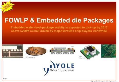
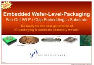
<strong>FOWLP</strong> & <strong>Embedded</strong> <strong>die</strong> <strong>Packages</strong><br />
© 2012<br />
<strong>Embedded</strong> wafer-level-package activity is expected to pick-up by 2015<br />
above $200M overall driven by major wireless chip players worldwide<br />
Infineon<br />
STATs ChipPAC<br />
Nokia<br />
Texas<br />
Instruments<br />
AT&S<br />
Copyrights © Yole Développement SA. All rights reserved.
© 2012 • 2<br />
Table of Content (1/2)<br />
• Scope of the Report & Definitions …...……. 4<br />
• Executive Summary ………………………… 11<br />
1) <strong>Embedded</strong> <strong>die</strong> in substrates of active ICs &<br />
passive components ………………….……. 48<br />
– Motivations and Drivers ………………... 49<br />
– Application focus for <strong>Embedded</strong> <strong>die</strong> package<br />
commercialization …………………..…... 64<br />
• Cell-phone & Consumer applications<br />
• Automotive applications<br />
• Medical applications<br />
– 2010-2020 market forecasts for <strong>Embedded</strong><br />
packages ………………………………….... 91<br />
• In Package shipments (M units)<br />
• In Packaging revenues ($M)<br />
– Supply chain emerging for embedded <strong>die</strong>s<br />
………………………………….…………….. 98<br />
• Players and position in the electronic value<br />
chain<br />
• Who is the most aggressive in<br />
commercialization?<br />
• Who is doing what: partnerships identified<br />
Copyrights © Yole Développement SA. All rights reserved.<br />
– Equt & Material Tool-Box for <strong>Embedded</strong> <strong>die</strong> . 129<br />
• Technology flavors for embedded package<br />
• Chip first versus chip last?<br />
• Single <strong>die</strong> embedding versus SiP module?<br />
• Challenges related to yield & supply chain<br />
– Cost structure for <strong>Embedded</strong> package<br />
manufacturing ………………………………….... 134<br />
• Comparison with competitive package alternative<br />
that <strong>Embedded</strong> <strong>die</strong> technology is looking for direct<br />
replacement (QFN, BGA, WLCSP, SOT, PoP…)<br />
• Cost structure target of <strong>Embedded</strong> <strong>die</strong> for different<br />
application cases (RFID, IPD, Power MOSFET /<br />
IGBT, DC/DC converters, PMU, Wireless<br />
Connectivity ICs, Digital Baseband, Memories, etc<br />
…)<br />
– Conclusion on “sweets spots” for the<br />
introduction of <strong>Embedded</strong> <strong>die</strong> technology in the<br />
short / medium / long term ……………………. 138<br />
FCI NXP
© 2012 • 3<br />
Table of Content (2/2)<br />
2) Fan-Out WLP technology development … 140<br />
– Motivations and market drivers …………... 144<br />
• Form factor, Cost and electrical performance<br />
• Thermal performance of <strong>FOWLP</strong> package<br />
compared to FC-BGA package solution<br />
– Supply chain emerging for <strong>FOWLP</strong> ……… 162<br />
• Players and position in the electronic value chain<br />
• Who is the most aggressive in commercialization?<br />
• Who is doing what: partnerships identified<br />
– 2010-2020 market forecasts for <strong>FOWLP</strong> type of<br />
packages ……………………………………... 174<br />
• In Package shipments (M units)<br />
• In epoxy wafer production (wspy eq.)<br />
• In Packaging revenues ($M)<br />
– <strong>FOWLP</strong> technologies & challenges …….. 202<br />
• Who owns the IP in this space?<br />
• 1 st generation versus 2 nd generation <strong>FOWLP</strong><br />
• “Passive integration with <strong>FOWLP</strong> technologies<br />
– Equipment & Materials for <strong>FOWLP</strong> ............ 213<br />
• Challenges in new material selection and missing<br />
equipment<br />
• Technology roadmap for <strong>FOWLP</strong> development<br />
– 2.5D integration trends based on <strong>FOWLP</strong> and<br />
silicon / glass interposer mix ……….……. 227<br />
Copyrights © Yole Développement SA. All rights reserved.<br />
– <strong>FOWLP</strong> patent activity summary …... 233<br />
– Cost structure for <strong>FOWLP</strong> ………..…. 265<br />
• Competitive package alternative that <strong>FOWLP</strong><br />
technology is looking for direct replacement<br />
• Cost structure for <strong>FOWLP</strong> by application<br />
– Evolution to Panel-scale-packaging .. 252<br />
• Conclusion & Perspectives ….………… 281<br />
• Appendix ……....…………….…..….…… 287<br />
– Yole Developpement company<br />
presentation & services<br />
StatsChipPAC
Wafer-Level<br />
Interface / Encapsulation<br />
LED & Sensors<br />
WLOptics<br />
© 2012 • 4<br />
3D WLP<br />
For MEMS & sensors<br />
(also called 3D SiP sometimes)<br />
Copyrights © Yole Développement SA. All rights reserved.<br />
Scope of the Report<br />
PANEL / Wafer-Scale-Packaging Platforms<br />
Wafer-Level<br />
Electrical Redistribution<br />
WL CSP<br />
‘Fan-in’<br />
<strong>FOWLP</strong><br />
‘Fan-out’<br />
<strong>Embedded</strong> <strong>die</strong><br />
in PCB / laminate<br />
� FOCUS of this report update<br />
Flip-chip & Wafer-Level<br />
Stacking / Integration<br />
3D IC<br />
& TSV<br />
Glass / Silicon<br />
2.5D<br />
interposers<br />
Flip-chip<br />
wafer bumping<br />
on BGA<br />
• Wafer-level-packaging encompass multiple different technology platform flavors<br />
but leverage similar type of process manufacturing know-how
© 2012 • 5<br />
Copyrights © Yole Développement SA. All rights reserved.<br />
Definitions<br />
• <strong>Embedded</strong> <strong>Packages</strong> refers to different concepts, IP, manufacturing infrastructures<br />
and related technologies. However, it is still possible to distinguish 2 main categories<br />
of embedded packages:<br />
<strong>Embedded</strong><br />
Wafer-Level-<strong>Packages</strong><br />
� based on a Molded Wafer infrastructure � based on a PCB / PWB substrate infrastructure<br />
NANIUM<br />
StatsChipPAC<br />
Wafer-Level Ball Grid Array<br />
eWLB<br />
Chip first<br />
UTCP<br />
Hidden <strong>die</strong><br />
IMB<br />
EMBIDS / EDC<br />
Imbera<br />
<strong>Embedded</strong> Active Module<br />
iQFN<br />
ECP – <strong>Embedded</strong> Component Packaging<br />
EOMIN
© 2012 • 6<br />
Objectives of the Report<br />
• This is the second report update on <strong>Embedded</strong> Wafer-Level-Packaging<br />
technologies and markets from Yole Developpement<br />
• The objectives of this first report are the following:<br />
– Analyze both <strong>FOWLP</strong> and <strong>Embedded</strong> <strong>die</strong> package technologies<br />
– Key market drivers, benefits and challenges by application<br />
– Market trends & figures with detailed breakdown by application<br />
– Technology roadmap and description of the complete manufacturing tool-box<br />
for embedded wafer-level-packaging:<br />
o Key equipment: for 200mm / 300mm / Panel manufacturing<br />
o Specific material selection coming from both FE / BE / PCB / LCD areas<br />
– Analysis of several embedded package target prices for a few key applications<br />
– Supply chain perspectives, key players and emerging infrastructure for<br />
embedded wafer-level-packaging<br />
o Analysis of the rationales behind the different possibilities of <strong>FOWLP</strong> and embedded<br />
<strong>die</strong> package implementation (chip first / chip last, single <strong>die</strong> / multi-<strong>die</strong> / SiP / PoP<br />
module, etc …)<br />
Copyrights © Yole Développement SA. All rights reserved.
© 2012 • 7<br />
Who should be Interested in this Report?<br />
• Integrated semiconductor Device<br />
Manufacturers and fabless IC companies<br />
– Benchmark the industrialization status of<br />
embedded packaging technologies within the<br />
industry<br />
– Identify possible partnerships or second<br />
source packaging subcontractors for your<br />
forthcoming developments<br />
• Assembly and Test Service companies<br />
– Get the list of the main companies interested<br />
in <strong>Embedded</strong> WLP<br />
– Screen possible new applications and<br />
technologies to support diversification<br />
strategy with embedded packaging platform<br />
• Equipment and Material suppliers<br />
– Understand the differentiated value of your<br />
products and technologies in this emerging<br />
but fast growing market<br />
– Identify new business opportunities and<br />
prospects<br />
Copyrights © Yole Développement SA. All rights reserved.<br />
• Electronic module makers and Original<br />
Equipment Makers<br />
– Evaluate the availability and benefits of using<br />
embedded package components in your end<br />
system<br />
– Monitor different embedded WLP suppliers<br />
to adjust your sourcing strategy<br />
• PCB and IC substrate manufacturers<br />
– Monitor the evolution of IC packaging,<br />
assembly and test, especially linked to<br />
emerging chip embedding<br />
– PCB-based technologies, <strong>FOWLP</strong>, IPD and<br />
3D interposers
© 2012 • 8<br />
Companies Cited in this Report<br />
3D-Plus, ADL Engineering, ADTEC Engineering, Amkor, ams, Analog<br />
Devices, AT&S, Aptos, Asahi Glass, ASE, ASM, Atotech, Broadcom,<br />
Bosch, Camtek, Casio Micronics, CIRETEC, CMK, Compass<br />
Technology, CSR, Datacon, Daeduck, Denso, Dialog Semiconductor,<br />
Dow Corning, DuPont Electronics, Dyconex, Epic, Epcos TDK,<br />
EVGroup, Fico Molding, Flip-chip International, Fraunhofer-IZM,<br />
Freescale, Fujitsu, HD Microsystems, HEICO, SK Hynix, Ibiden,<br />
Imbera, IME, IMEC, Infineon, Invensas, IPDiA, ITRI, King Dragon<br />
International, KYEC, Leti, Lintec, LG Electronic, Micron, MicroChem,<br />
Mitsui, Murata, Nagase ChemteX, NANIUM, NEC Electronics, Nitto<br />
Denko, Nokia, NSC, NXP, OptoPac Oki Electric, ORC, Panasonic,<br />
PPT, Qualcomm, Renesas, Rohm & Hass, Rudolph technologies,<br />
Samsung, SEMCO, Shinko Electric, SPIL, STATS ChipPAC, ST-<br />
Ericsson, STMicroelectronics, SPTS, SMIC, Shin-Etsu, SÜSS<br />
Microtec, Taiyo Yuden, TDK, Tessera, Texas Instruments, tok, Tong<br />
Hsing, Toray chemical, Toray Engineering, Toshiba, Towa, Triquint,<br />
UMTC, Unimicron, Unovis, UTAC, Vertical Circuits, Wolfson<br />
Microelectronics, Yamada and more…<br />
Copyrights © Yole Développement SA. All rights reserved.
Jerome Baron<br />
© 2012 • 9<br />
About the authors of this report<br />
– Jerome is the business unit<br />
manager of the semiconductor<br />
packaging market research at<br />
Yole Developpement. He has<br />
been following the 3D packaging<br />
market evolution since its early<br />
beginnings at the device,<br />
equipment and material levels.<br />
He was granted a Master of<br />
Science degree from INSA-Lyon<br />
in France as well as a Master of<br />
Research from INL – Lyon<br />
Institute of Nanotechnology<br />
Contact: baron@yole.fr<br />
Copyrights © Yole Développement SA. All rights reserved.<br />
Lionel Cadix<br />
– Lionel joined Yole after the<br />
completion of several projects<br />
linked to the<br />
characterization and modeling of<br />
high density TSV and 3DIC chip<br />
stacking in collaboration<br />
with CEA-Leti and<br />
STMicroelectronics during his<br />
PhD. He is author of several<br />
publications and 8 patents in<br />
the field of 3D Integration<br />
Contact: cadix@yole.fr
Concepts of <strong>FOWLP</strong> / <strong>Embedded</strong> di in package<br />
• Two types of <strong>Embedded</strong> Wafer-level-packages are emerging<br />
© 2012 • 10<br />
– <strong>FOWLP</strong> is based on a reconfigured molded wafer infrastructure<br />
– <strong>Embedded</strong> <strong>die</strong> in package is based on a PCB type of Panel infrastructure<br />
FO MCP<br />
<strong>FOWLP</strong><br />
1 st generation<br />
NANIUM<br />
FO PoP<br />
Copyrights © Yole Développement SA. All rights reserved.<br />
AT&S<br />
FO SiP<br />
<strong>Embedded</strong> MCP<br />
Courtesy of AT&S<br />
<strong>Embedded</strong> PoP<br />
<strong>Embedded</strong> <strong>die</strong><br />
Single chip<br />
<strong>Embedded</strong> SiP
© 2012 • 11<br />
spacing<br />
Chip embedding<br />
<strong>FOWLP</strong><br />
Chip Embedding / Fan-Out WLP<br />
Geometry definitions<br />
width Line Spacing / Width (µm)<br />
Courtesy of AT&S<br />
Courtesy of NANIUM<br />
• Shift in manufacturing technologies is expected<br />
– Geometries of the two emerging packaging technologies will shrink with time as to allow for higher<br />
routing density, highly integrated passive inductors and baluns, and integration of ICs with no prior<br />
RDL on the device wafer<br />
– There is a move (at least for fan-out WLP) from currently used mask aligners to front-end steppers to<br />
support this reduction of the feature sizes<br />
Copyrights © Yole Développement SA. All rights reserved.<br />
1 st generation<br />
(up to 2012)<br />
2 nd generation<br />
(2012-2014)<br />
3 rd generation<br />
(2014-2020)<br />
40/40 25/25 15/15<br />
20/20 10/10 5/5
<strong>FOWLP</strong> / <strong>Embedded</strong> Die Packaging Roadmap<br />
SOT / TSOP<br />
© 2012 • 12<br />
MOSFET<br />
QFN<br />
IPD<br />
WL CSP<br />
RF connectivity, PMU, Analog<br />
FC BGA<br />
RF Transceiver, Baseband<br />
WB BGA<br />
PMU<br />
Copyrights © Yole Développement SA. All rights reserved.<br />
<strong>Embedded</strong> <strong>die</strong><br />
Micro-SiP module<br />
� RFID, thin-film IPD, MOSFET,<br />
IGBT, DC-DC converters, IC drivers,<br />
MEMS & Sensors , RFEM…<br />
<strong>FOWLP</strong><br />
FO MCP<br />
� Digital Baseband SOC<br />
� RF Transceiver<br />
� NFC / Connectivity SOC<br />
� ASIC / DSP / FPGA<br />
� Specific Analog IC & Sensors<br />
MATURE tech EMERGING tech FUTURE tech<br />
(2000 - 2010) (2008 - 2014) (> 2014 - 2018)<br />
<strong>Embedded</strong> MCP<br />
� Power modules, IPD<br />
protection network modules<br />
Digital / Analog partitioning …<br />
<strong>Embedded</strong> PoP<br />
� Digital + memory modules,<br />
Analog + Digital + memory<br />
modules, Sensor modules,<br />
Radio FEM module …<br />
FO PoP<br />
� Digital + memory modules,<br />
Analog + Digital + memory<br />
modules, Sensor modules …<br />
FO SiP<br />
� RF connectivity modules,<br />
Audio modules, Sensor<br />
modules, Radio modules …
© 2012 • 13<br />
Narrow commercialization window<br />
of present eWLB / <strong>FOWLP</strong> 1 st generation technology<br />
FO-MCP / SiP<br />
(for analog / digital SOC partitioning)<br />
• As of today (2012), the commercialization eWLB / <strong>FOWLP</strong> 1 st generation technology is quite<br />
restricted to a quite narrow application window from 40-300 IO pin-counts, 4x4 to 7x7mm2<br />
package body size<br />
– Package / devices below 4x4mm2 and 40 IOs: <strong>FOWLP</strong> will struggle to compete with Wire-bonded<br />
BGA/leadframe, <strong>Embedded</strong> <strong>die</strong> package and 3DIC wafer-to-wafer assembly platform � An extra niche to be<br />
found by developing FO-MCP / SiP platform here<br />
– Package / devices of more than 15x15mm²: flip-chip and 2.5D interposer are the best packaging solutions<br />
today � new flip-chip and 2.5D version of <strong>FOWLP</strong> technology will be adapted to compete on cost<br />
– Between 4x4mm2 and 15x15mm²: the solutions are not yet decided and the battle is hard between most<br />
every packaging technique � and this is where the biggest part of the IC packaging business is in volume!<br />
Copyrights © Yole Développement SA. All rights reserved.<br />
<strong>FOWLP</strong><br />
(commercialized TODAY)<br />
FO-PoP (for BB/APE)<br />
2.5D <strong>FOWLP</strong><br />
(for APE / ASIC + memory + analog)<br />
Flip-chip <strong>FOWLP</strong><br />
(for large <strong>die</strong> ASIC / FPGA)<br />
4 – 10 IOs 10 – 40 IOs 40 – 300 IOs 300 – 700 IOs 700 – 1000’s IOs<br />
I/O#<br />
numbers<br />
2x2 mm2 4x4 mm2 7x7 mm2<br />
15x15 mm2 25x25 mm2 package<br />
<strong>Embedded</strong> <strong>die</strong><br />
3DIC (W2W) FC-CSP / BGA<br />
2.5D interposers (C2W)<br />
body size<br />
WB BGA /<br />
QFN / TSOP<br />
Logic n Logic n+1 Logic n+2 Logic n+3
FC BGA<br />
<strong>Embedded</strong><br />
<strong>die</strong> in PCB<br />
© 2012 • 14<br />
Packaging Value Chain Comparison*<br />
Comparison ratio of the packaging, assembly & test value<br />
Substrate Supplier<br />
<strong>FOWLP</strong><br />
Substrate Supplier<br />
& Assembly<br />
Copyrights © Yole Développement SA. All rights reserved.<br />
Inventory<br />
Wafer Fab<br />
(RDL)<br />
Wafer<br />
Bumping<br />
Wafer Fab + <strong>FOWLP</strong><br />
assembly<br />
Assembly & Test<br />
20% 25% 10% 45%<br />
Wafer<br />
Test +<br />
Final<br />
Test<br />
85% 15%<br />
Wafer Fab<br />
(RDL & Cu pad)<br />
Wafer Test<br />
+ Final<br />
Test<br />
55% 30% 15%<br />
• New shift in the packaging, assembly & test value chains<br />
* Comparison<br />
scenario for the<br />
case of 64 I/Os,<br />
0.4mm pitch IC<br />
PRODUCT<br />
PRODUCT<br />
PRODUCT<br />
– <strong>FOWLP</strong> implies a simplification and consolidation of the packaging, assembly & test in a “Mid-end”<br />
type of infrastructure<br />
– <strong>Embedded</strong> <strong>die</strong> packaging opens the door to substrate suppliers to realize themselves the whole<br />
packaging, assembly and test on a Panel “PCB based” infrastructure
Package IC Co-Design is Necessary Before <strong>Embedded</strong> WLP<br />
© 2012 • 15<br />
SERIAL IC Design Package IC Co-Design<br />
Digital IC design<br />
Tool A<br />
Tool B<br />
Analog IC design<br />
Tool C<br />
Tool D<br />
Manufacturing<br />
PRODUCT<br />
Packaging design<br />
Substrate<br />
Package outline<br />
FE/BE process<br />
Copyrights © Yole Développement SA. All rights reserved.<br />
FE / BE Manufacturing<br />
Analog IC<br />
design<br />
Packaging<br />
development<br />
PRODUCT<br />
Digital IC<br />
design<br />
DfM � Designed for manufacturing<br />
Infrastructure � Common Tool-Box<br />
• Package IC co-design drives to silicon <strong>die</strong> and process optimization, for e.g.<br />
– to avoid RDL at the IC wafer level before the embedded WLP process<br />
– RF chip package co-design is also necessary to integrate to take package parasitics into accounts
<strong>Embedded</strong> <strong>die</strong> in<br />
package<br />
(Single chip modules)<br />
X<br />
© 2012 • 16<br />
X<br />
Casio / CMK – Watch module<br />
<strong>Embedded</strong> Wafer-Level-<strong>Packages</strong><br />
Status of commercialization<br />
<strong>FOWLP</strong><br />
1 st generation / single <strong>die</strong><br />
X Broadcom – ASIC<br />
StatsChipPAC<br />
X Altera – FPGA<br />
X STEricsson – RF Transceivers<br />
X IFX / Intel Mobile – Wireless Baseband SOC<br />
X Maxim IC – PMU<br />
X SST – EEPROM memories<br />
X Renesas – ASIC X Toshiba – FPGA<br />
Murata – Cellular terrestrial digital module<br />
Copyrights © Yole Développement SA. All rights reserved.<br />
<strong>Embedded</strong> <strong>die</strong><br />
SiP / PoP module<br />
packages<br />
2 nd generation<br />
<strong>FOWLP</strong><br />
X TI – DC/DC converter<br />
NXP – RFID / IPD modules<br />
2006 2007 2008 2009 2010 2012 2014 2016 2018<br />
X<br />
X<br />
FO SiP<br />
X<br />
X<br />
ADI<br />
X<br />
X Infineon<br />
X ams<br />
X<br />
X<br />
FO MCP<br />
FO PoP<br />
<strong>Embedded</strong> SiP <strong>Embedded</strong> PoP<br />
Rohm – DC/DC converter<br />
X<br />
X<br />
X<br />
X<br />
X<br />
X
First eWLB Package in High Volume Production!<br />
• First design win for eWLB<br />
© 2012 • 17<br />
– Infineon (GE) was the first company<br />
to commercialize its own eWLB<br />
packaging technology in an LGE<br />
cell-phone in early 2009<br />
– ASE, StatsChipPAC have been<br />
qualified as subcontractors<br />
for eWLB manufacturing<br />
– Infineon’s chip is a wireless<br />
baseband SOC<br />
with multiple<br />
integrated functions<br />
(GPS, FM radio, BT…)<br />
– Same eWLB<br />
product is now in<br />
production in<br />
some Nokia<br />
handsets<br />
since 2010<br />
Copyrights © Yole Développement SA. All rights reserved.<br />
First eWLB<br />
package with<br />
Infineon’s<br />
wireless<br />
Baseband SOC<br />
was found in<br />
an LG cellphone<br />
(Reverse<br />
Engineering<br />
pictures courtesy<br />
of SystemPlus<br />
Consulting and<br />
Binghamton<br />
University )
Current end-products using eWLB / <strong>FOWLP</strong><br />
• Mobile and wireless applications using FO-WLP packaging<br />
© 2012 • 18<br />
– LGE was the first OEM to integrate the eWLB to the wireless baseband in the following models<br />
• PMB8810 phone, T310 phone, T300 phone, GD350 phone, GB220 phone, GB230 phone, GS170 phone, GU230 phones<br />
– We can also find eWLB in Samsung cell phones (baseband modem)<br />
• S3350 phone, Galaxy Tab tablet, Galaxy S phones<br />
– Some Nokia’s phones use eWLB for the baseband modem and RF tranceiver<br />
• S30 series platform (2010 phone version), S40 series platform (2010 phone version), 1 smart-phone line (to be identified)<br />
2009 2010 2011<br />
• Extension of the technology platform to a wider field of application areas is in<br />
preparation<br />
– FO-WLP is expected to be integrated as well as some point in the automotive and medical<br />
applications<br />
Copyrights © Yole Développement SA. All rights reserved.
FO-WLP Revenues (M $)<br />
$0M<br />
2008 2009 2010 2011 2012F 2013F 2014F 2015F 2016F 2017F 2018F 2019F 2020F<br />
TOT <strong>FOWLP</strong> (M$) $13M $48M $75M $107M $114M $107M $118M $195M $280M $374M $477M $571M $641M<br />
© 2012 • 19<br />
<strong>FOWLP</strong> activity market evolution & forecast<br />
$700M<br />
$600M<br />
$500M<br />
$400M<br />
$300M<br />
$200M<br />
$100M<br />
Copyrights © Yole Developpement SA. All rights reserved.<br />
<strong>FOWLP</strong> activity Revenues (M$)<br />
Overall evolution since eWLB technology introduction<br />
Yole Developpement © October 2012<br />
Intel Mobile /<br />
IFX eWLB driven<br />
Transition phase<br />
CAGR ~ 0%<br />
Ramp-up with fab-less wireless<br />
IC players and wide <strong>FOWLP</strong><br />
infrastructure / supply-chain<br />
• After growing fast since Infineon / Intel Mobile’s push for eWLB technology commercialization, the <strong>FOWLP</strong><br />
market activity reached the $100M market valuation last year<br />
– This young industry will probably need to wait for 2015 – 2016 time frame to reach the $250M market valuation as the technology<br />
to ramp-up in HVM, the demand moving from IDMs to fab-less wireless IC players (such as Qualcomm, Broadcom, Mediatek,<br />
etc…) and supported by a solid infrastructure and supply-chain of OSATs
© 2012 • 20<br />
Optimistic scenario (1/2)<br />
• To bend the rules, we decided in this report to propose an alternative scenario for <strong>FOWLP</strong><br />
market evolution<br />
• Indeed, regarding the numerous rumors linked to this space, several feedbacks pushed us<br />
to propose an optimistic forecast model, making the market starting growing fast as soon as<br />
2013<br />
• This enthousiastic scenario would be linked to the following players’ activity<br />
– Spreadtrum (CN)<br />
– Maxim (US)<br />
– ADL (TW)<br />
– Mediatek (TW)<br />
• In this alternative model<br />
– A 30% penetration rate have been<br />
applied for <strong>FOWLP</strong> as soon as<br />
2013, for existing products already<br />
using this platform<br />
• Digital Baseband Processor<br />
• APE/BB wireless SoC<br />
– Volume production for the other<br />
applications would start 1 year<br />
sooner than in our initial model (for<br />
RF tranceiver, PMU, ASIC,<br />
Touchscreen Controller, RF<br />
Connectivity devices)<br />
Copyrights © Yole Developpement SA. All rights reserved.<br />
FO-WLP Revenues (M $)<br />
1 200<br />
1 000<br />
800<br />
600<br />
400<br />
200<br />
0<br />
<strong>FOWLP</strong> Revenues (optimistic scenario)<br />
Breakdown by application area (M$)<br />
Yole Developpement © October 2012<br />
2010 2011 2012 2013 2014 2015 2016 2017 2018 2019 2020<br />
Medical<br />
Automotive<br />
Industrial<br />
Consumer<br />
Mobile - Wireless
Wafer count (12’’eq. wafers) Millions<br />
3.0<br />
2.5<br />
2.0<br />
1.5<br />
1.0<br />
0.5<br />
0.0<br />
© 2012 • 21<br />
Optimistic scenario (2/2)<br />
Yole Developement © October 2012<br />
2010 2011 2012 2013 2014 2015 2016 2017 2018 2019 2020<br />
Copyrights © Yole Developpement SA. All rights reserved.<br />
<strong>FOWLP</strong> wafer forecast (optimistic scenario)<br />
Breakdown by IC type (12’’eq wafers)<br />
DRAM<br />
Touchscreen Controller<br />
RF Connectivity Combo<br />
PMU<br />
NAND Flash Memory<br />
Memory Controller<br />
MEMS & Sensors<br />
NFC<br />
RF Tranceiver<br />
ASIC / FPGA<br />
Audio/Video Codec<br />
Digital Baseband Processor<br />
BB/APE wireless SoC<br />
• According to this model the market would grow at a 30% CAGR on the 2010-2020 time frame,<br />
leading to a ~ $1B market in 2020<br />
• It would lead to nearly 500,000 wafers shipped in 2020 and more than 2.8 billion in 2020<br />
• Now we just have to wait and see if the rumors come true and if the infrastructure of this<br />
young industry will be strong enough to support this fast growing evolution
<strong>FOWLP</strong> 2011 revenues market shares (in M$)<br />
© 2012 • 22<br />
<strong>FOWLP</strong> 2011 revenues market shares (in M$)<br />
Breakdown between main players<br />
ASE (Tw)<br />
$14M<br />
13%<br />
NANIUM (Pt)<br />
$41M<br />
38%<br />
• NANIUM (Pt) and STATschipPAC (Sg) shares more than 80% of the activity, mainly driven by<br />
Intel Mobile volume demand on eWLB production<br />
– ASE (Tw) is shutting down its 200mm eWLB line. Other OSATs have qualified other <strong>FOWLP</strong> technologies<br />
such as ADL (Tw), Amkor (Kr) and NEPES (Sg)<br />
– Additional packaging houses are coming on board as well such as TSMC (Tw), SPIL (Tw) and J-Devices (Jp)<br />
Copyrights © Yole Developpement SA. All rights reserved.<br />
Others *<br />
$6M<br />
6%<br />
TOT<br />
~$107M<br />
* Others: ADL (Tw),<br />
Amkor (Kr), NEPES (Sg)<br />
STATSChipPAC (Sg)<br />
$46M<br />
43%<br />
Yole Developpement ©<br />
October 2012
PANEL Infrastructure for <strong>Embedded</strong> Chip Packaging<br />
• <strong>Embedded</strong> <strong>die</strong> packaging technology will leverage an entirely new infrastructure<br />
based on large PANEL, low cost PCB manufacturing techniques!<br />
© 2012 • 23<br />
– Typically able to integrate more than 10,000 – 40,000 <strong>die</strong>s per panel!<br />
Courtesy of AT&S<br />
Copyrights © Yole Développement SA. All rights reserved.<br />
� AT&S’s first generation production is based on 18x24 sq.<br />
inch panels. 2 nd gen on 21x24 sq. inch panels!
AT&S step into HVM for <strong>Embedded</strong> MicroSiP packages<br />
• Texas Instruments (US) is the first customer to qualify into HVM<br />
the embedded <strong>die</strong> package line of AT&S<br />
– First application is a DC-DC converter MicroSiP module:<br />
Teardowns courtesy of SystemPlus Consulting<br />
© 2012 • 24<br />
Copyrights © Yole Developpement SA. All rights reserved.
DNP’s <strong>Embedded</strong> active & passive substrate in HVM<br />
• DNP (JP) is supplying Sony’s camera module with embededded passive and active<br />
components in HVM since 2010 already<br />
– Auto-focus driver IC and DC-DC converter WLCSP <strong>die</strong>s are placed within the coreless cavity substrate<br />
© 2012 • 25<br />
Copyrights © Yole Développement SA. All rights reserved.<br />
Teardowns courtesy of SystemPlus Consulting
<strong>Embedded</strong> <strong>die</strong> package PANEL infrastructure Roadmap<br />
Substrate<br />
players driven<br />
2010 - 2012 2013 2014 2015 > 2016<br />
© 2012 • 26<br />
OSAT<br />
players driven<br />
4”x20” – 102x508mm /<br />
PCB laminate substrate<br />
1/4 PANEL<br />
Copyrights © Yole Développement SA. All rights reserved.<br />
YIELD % to increase<br />
POWER & ANALOG<br />
small SiP module applications:<br />
- DC/DC converter<br />
- IPD<br />
- AF driver<br />
- Small ASICs<br />
- MOSFET<br />
- IGBT<br />
- RFID<br />
8”x20” – 204x508mm /<br />
PCB laminate substrate<br />
1/2 PANEL<br />
DIGITAL<br />
thin PoP module applications<br />
- BB / APE<br />
YIELD % to increase<br />
YIELD % to increase<br />
16”x20” – 400x505mm /<br />
PCB laminate substrate<br />
RF & MIXED SIGNAL<br />
large SiP module applications :<br />
- PMU / PMIC<br />
- RFEM (SAW, PA, etc…)<br />
- RF connectivity (WLAN/BT/FM)<br />
- Audio/Video Codec<br />
Full<br />
PANEL<br />
RF & MIXED SIGNAL<br />
SiP module applications :<br />
- PMU / PMIC<br />
- RFEM<br />
- RF connectivity (WLAN/BT/FM)<br />
- Audio/Video Codec
© 2012 • 27<br />
First Conclusions on <strong>Embedded</strong> Wafer-Level-<strong>Packages</strong><br />
• 1st generation <strong>FOWLP</strong> and <strong>Embedded</strong> <strong>die</strong> packages is a high volume reality and the two<br />
infrastructures are now clearly settled and proven in HVM in each of their very different<br />
application space<br />
– Today, first generations of <strong>Embedded</strong> <strong>die</strong> package and <strong>FOWLP</strong> technologies are not really competing<br />
at all as they are driven by different players and initially target very different applications.<br />
• However, this situation will totally change in the future with “2nd generation” derivatives of<br />
the technologies that are currently under development for future SiP and PoP module<br />
realizations, likely on larger format<br />
– We are likely to be witness to a fascinating battle in the years to come in the 3D Packaging space with<br />
on one hand, embedded <strong>die</strong> packaging technologies supported by large panel PCB infrastructure and<br />
<strong>FOWLP</strong> technologies on the other hand, which is looking for moving to larger wafer format, likely<br />
square 300mm PANEL first and possibly later on larger PANEL mixing PCB, semiconductor backend,<br />
semiconductor WLP and LCD large area processing know-how<br />
Copyrights © Yole Développement SA. All rights reserved.
© 2012 • 28<br />
Copyrights © Yole Développement SA. All rights reserved.<br />
Yole Developpement<br />
Company Presentation
© 2012 • 29<br />
Fields of research activity<br />
• Yole Developpement is a market research and strategy consulting<br />
company, founded in 1998. We are involved in the following areas:<br />
Advanced<br />
Packaging<br />
Microfluidic<br />
& Bio-tech<br />
LED &<br />
Compound Semi<br />
• Yole Développement has 25 full time analysts, with both technical and<br />
marketing/management background and operate worldwide since 1998<br />
Copyrights © Yole Développement SA. All rights reserved.<br />
MEMS &<br />
Sensors<br />
Power<br />
Electronics<br />
Photovoltaic
© 2012 • 30<br />
Our Global Presence & Activity<br />
30% of our activity is<br />
in North America<br />
Yole Inc.<br />
� perkins@yole.fr<br />
Copyrights © Yole Développement SA. All rights reserved.<br />
40% of our activity is in<br />
EU Countries<br />
Yole Europe<br />
� eloy@yole.fr<br />
Yole Développement<br />
Lyon (HQ).<br />
Yole Korea<br />
� yang@yole.fr<br />
30% of our activity is<br />
in Asia<br />
Yole Japan<br />
Yole Taiwan<br />
� katano@yole.fr<br />
� meiling.tsai@yole.com.tw
© 2009<br />
HB-LED LED Packaging<br />
Market Technology & Technology & Market Trends<br />
Osram<br />
IR<br />
Copyrights © Yole Développement SARL. All rights reserved.<br />
TSV+<br />
Cost Analysis Tool for<br />
your 3D IC manufacturing<br />
© 2012 • 31<br />
TSV Scenario Cost structure breakdown<br />
$168<br />
41%<br />
1995<br />
Sidebraze DIP<br />
$27<br />
7% $23<br />
6%<br />
$8<br />
$31<br />
$9 $37 2%<br />
7%<br />
2% 9%<br />
$109<br />
26%<br />
Via / Etching Drilling<br />
Via Isolation<br />
Via filling<br />
Temporary bonding<br />
Thinning<br />
Stress release<br />
BEOL (Pads)<br />
Bonding<br />
© 2010<br />
~125 sq mm ~100 sq mm ~25 sq mm<br />
1996-2002<br />
1999 - today 2006<br />
Plastic PDIP<br />
FO WLP &<br />
<strong>Embedded</strong> <strong>die</strong><br />
Our latest advanced packaging<br />
market research reports<br />
SMT SOIC<br />
& Die Down<br />
MEMS Packaging<br />
Market & Technology Trends<br />
Stacked Die<br />
QFN<br />
6 & 6 mm<br />
WL CSP<br />
2012 Report update<br />
Copyrights © Yole Développement SA. All rights reserved.<br />
1995<br />
Sidebraze DIP<br />
Copyrights © Yole Développement SA. All rights reserved.<br />
~125 sq mm ~100 sq mm ~25 sq mm<br />
1996-2002<br />
1999 - today 2006<br />
Plastic PDIP<br />
Wafer Packaging Fabs<br />
DATABASE<br />
N<br />
o<br />
k<br />
i<br />
a<br />
SMT SOIC<br />
& Die Down<br />
N<br />
o<br />
k<br />
i<br />
a<br />
3D IC & TSV<br />
2010 Market Analysis<br />
F<br />
r<br />
e<br />
s<br />
c<br />
a<br />
l<br />
e<br />
Stacked Die<br />
QFN<br />
6 & 6 mm<br />
2.5D Glass & Silicon<br />
interposers - 2010 Report<br />
© 2010<br />
Equipment Advanced Packaging<br />
& Materials<br />
for 3DIC & Wafer-Level-Packaging<br />
EVG<br />
Equipment & Materials<br />
S<br />
i<br />
l<br />
e<br />
x<br />
D<br />
u<br />
P<br />
o<br />
n<br />
t<br />
DuPont<br />
NEC-Schott<br />
SUSS STS<br />
Brewer Science<br />
I<br />
M<br />
E<br />
C<br />
Copyrights © Yole Développement SARL. All rights reserved.<br />
N<br />
o<br />
k<br />
i<br />
a<br />
Via First / Via Last?<br />
3D integration Scenarios<br />
F<br />
r<br />
e<br />
s<br />
c<br />
a<br />
l<br />
e<br />
IPD - Thin-film<br />
Integrated Passive Devices<br />
S<br />
i<br />
l<br />
e<br />
x<br />
D<br />
u<br />
P<br />
o<br />
n<br />
t<br />
Flip-chip<br />
2011 Report<br />
I<br />
M<br />
E<br />
C
© 2012 • 32<br />
Copyrights © Yole Développement SA. All rights reserved.<br />
To contact us


