American Ceramic Society Bulletin
American Ceramic Society Bulletin
American Ceramic Society Bulletin

Create successful ePaper yourself
Turn your PDF publications into a flip-book with our unique Google optimized e-Paper software.
advances in nanomaterials<br />
Perovskite-based tunable superlens developed<br />
The DOE’s Lawrence Berkeley<br />
National Lab says its staffers have<br />
developed a novel mode of fabricating<br />
a superlens for the infrared spectrum<br />
using, for the first time, perovskitebased<br />
oxides. The lab says a group led<br />
by Ramamoorthy Ramesh has reported<br />
on its “Near-field examination of<br />
perovskite-based superlenses and superlens-enhanced<br />
probe-object coupling”<br />
in Nature Communications (doi:10.1038/<br />
ncomms1249).<br />
The innovation is an alternative to<br />
super resolution imaging approaches<br />
that are based on metamaterials. In<br />
brief, metamaterials are difficult to<br />
make and absorb a lot of precious light<br />
energy.<br />
According to the lab’s release, “The<br />
perovskite-based oxides on the other<br />
hand are simpler and easier to fabricate<br />
and are ideal for capturing light in the<br />
mid-infrared range. This opens the door<br />
to highly sensitive biomedical detection<br />
and imaging. It is also possible that the<br />
superlensing effect can be selectively<br />
turned on/off, which would open the<br />
door to highly dense data writing and<br />
storage.”<br />
The group says it is able to achieve<br />
an imaging resolution of λ/14 at the<br />
superlensing wavelength.<br />
One of the biggest challenges for<br />
the researchers according to the report<br />
was finding the right combination of<br />
perovskites that would make an effective<br />
superlens. What they landed on<br />
was a layer of bismuth ferrite and a<br />
layer of strontium titanate with thicknesses<br />
of 200 and 400 nanometers,<br />
respectively. These thin films were<br />
grown by pulsed-laser deposition.<br />
In the lab’s release, Susanne<br />
Kehr, now with the University of St.<br />
Andrews (Scotland) and Yongmin Liu,<br />
a metamaterials expert at Berkeley’s<br />
NSF Nanoscale Science and Engineering<br />
Center, provide additional<br />
information about the advantages of<br />
perovskites. “The bismuth ferrite and<br />
strontium titanate material feature a<br />
<strong>American</strong> <strong>Ceramic</strong> <strong>Society</strong> <strong>Bulletin</strong>, Vol. 90, No. 4<br />
low rate of photon absorption and can<br />
be grown as epitaxial multilayers whose<br />
highly crystalline quality reduces interface<br />
roughness so there are few photons<br />
lost to scattering,” they say. “This combination<br />
of low absorption and scattering<br />
losses significantly improves the<br />
imaging resolution of the superlens.”<br />
This research was conducted by an<br />
international collaboration of scientists,<br />
including ACerS member Lane Martin<br />
at the University of Illinois, Champaign-Urbana.<br />
Because of thickness and related<br />
wavelength issues, these investigators<br />
sought and found a way to gain detailed<br />
control over the superlens, selective<br />
tuning sections or toggling the effect<br />
via an external electric field.<br />
“The ability to switch superlensing<br />
on and off for a certain wavelength<br />
with an external electric field would<br />
make it possible to activate and deactivate<br />
certain local areas of the lens,”<br />
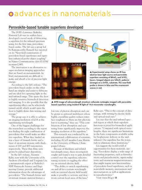
(Credit: Kehr, et. al.)<br />
▲ Experimental setup shows an IR freeelectron<br />
laser light source and perovskite<br />
superlens consisting of BiFeO 3 and SrTiO 3<br />
layers. Imaged objects are SrRuO 3 patterns<br />
(orange) on a SrTiO 3 substrate. The near-field<br />
probe is shown in blue and the evanescent<br />
waves in red.<br />
▲ AFM image of subwavelength strontium ruthenate rectangles imaged with perovskitebased<br />
superlens using incident IR light of 14.6 micrometer wavelengths.<br />
Kehr says. “This is the concept of datastorage,<br />
with writing by electric fields<br />
and optical read-outs.”<br />
Liu says that the mid-infrared spectral<br />
region at which their superlens<br />
functions is prized for biomedical applications.<br />
“Compared with optical wavelengths,<br />
there are significant limitations<br />
in the basic components available today<br />
for biophotonic delivery in the midinfrared.<br />
Our superlens has the potentials<br />
to eliminate these limitations.”<br />
Liu suggests the world is full of<br />
opportunities for these materials, saying,<br />
“Perovskites display a wide range of<br />
fascinating properties, such as ferroelectricity<br />
and piezoelectricity, superconductivity<br />
and enormous magnetoresistance,<br />
that might inspire new functionalities<br />
of perovskite-based superlenses, such as<br />
nonvolatile memory, microsensors and<br />
microactuators, as well as applications<br />
in nanoelectronics.”<br />
Visit: www.lbl.gov n<br />
(Credit: Kehr, et. al.)<br />
15