Breakthroughs Breakthroughs - ETH - Ultrafast Laser Physics
Breakthroughs Breakthroughs - ETH - Ultrafast Laser Physics
Breakthroughs Breakthroughs - ETH - Ultrafast Laser Physics

You also want an ePaper? Increase the reach of your titles
YUMPU automatically turns print PDFs into web optimized ePapers that Google loves.
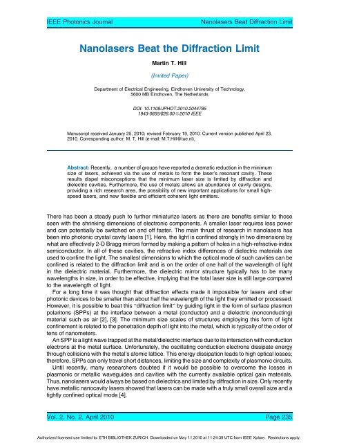
IEEE Photonics Journal Nanolasers Beat Diffraction Limit<br />
Nanolasers Beat the Diffraction Limit<br />
Martin T. Hill<br />
(Invited Paper)<br />
Department of Electrical Engineering, Eindhoven University of Technology,<br />
5600 MB Eindhoven, The Netherlands<br />
DOI: 10.1109/JPHOT.2010.2044785<br />
1943-0655/$26.00 Ó2010 IEEE<br />
Manuscript received January 25, 2010; revised February 19, 2010. Current version published April 23,<br />
2010. Corresponding author: M. T. Hill (e-mail: M.T.Hill@tue.nl).<br />
Abstract: Recently, a number of groups have reported a dramatic reduction in the minimum<br />
size of lasers, achieved via the use of metals to form the laser’s resonant cavity. These<br />
results dispel misconceptions that the minimum laser size is limited by diffraction and<br />
dielectric cavities. Furthermore, the use of metals allows an abundance of cavity designs,<br />
providing a rich research area, the possibility of new important applications for small highspeed<br />
lasers, and new flexible and efficient coherent light emitters.<br />
There has been a steady push to further miniaturize lasers as there are benefits similar to those<br />
seen with the shrinking dimensions of electronic components. A smaller laser requires less power<br />
and can potentially be switched on and off faster. The main thrust of research in nanolasers has<br />
been into photonic crystal cavity lasers [1]. Here, the light is confined strongly in two dimensions by<br />
what are effectively 2-D Bragg mirrors formed by making a pattern of holes in a high-refractive-index<br />
semiconductor. In all of these cavities, the refractive index differences of dielectric materials are<br />
used to confine the light. The smallest dimensions to which the optical mode of such cavities can be<br />
confined is related to the diffraction limit and is on the order of one half of the wavelength of light<br />
in the dielectric material. Furthermore, the dielectric mirror structure typically has to be many<br />
wavelengths in size, in order to be effective, implying that the total laser size is still large compared<br />
to the wavelength of light.<br />
For a long time it was thought that diffraction effects made it impossible for lasers and other<br />
photonic devices to be smaller than about half the wavelength of the light they emitted or processed.<br />
However, it is possible to beat this Bdiffraction limit[ by guiding light in the form of surface plasmon<br />
polaritons (SPPs) at the interface between a metal (conductor) and a dielectric (nonconducting)<br />
material such as air [2], [3]. The minimum size scales of structures employing this form of light<br />
confinement is related to the penetration depth of light into the metal, which is typically of the order of<br />
tens of nanometers.<br />
An SPP is a light wave trapped at the metal/dielectric interface due to its interaction with conduction<br />
electrons at the metal surface. Unfortunately, the oscillating conduction electrons dissipate energy<br />
through collisions with the metal’s atomic lattice. This energy dissipation leads to high optical losses;<br />
therefore, SPPs can only travel short distances, limiting the size and complexity of plasmonic circuits.<br />
Until recently, many researchers doubted if it would be possible to overcome the losses in<br />
plasmonic or metallic waveguides and cavities with the currently available optical gain materials.<br />
Thus, nanolasers would always be based on dielectrics and limited by diffraction in size. Only recently<br />
have metallic nanocavity lasers showed that lasers can be made with a truly small overall size and a<br />
tightly confined optical mode [4].<br />
Vol. 2, No. 2, April 2010 Page 235<br />
Authorized licensed use limited to: <strong>ETH</strong> BIBLIOTHEK ZURICH. Downloaded on May 11,2010 at 11:24:39 UTC from IEEE Xplore. Restrictions apply.