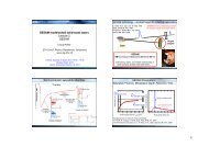
Breakthroughs Breakthroughs - ETH - Ultrafast Laser Physics
Breakthroughs Breakthroughs - ETH - Ultrafast Laser Physics
Breakthroughs Breakthroughs - ETH - Ultrafast Laser Physics

You also want an ePaper? Increase the reach of your titles
YUMPU automatically turns print PDFs into web optimized ePapers that Google loves.
IEEE Photonics Journal <strong>Breakthroughs</strong> in Silicon Photonics 2009<br />
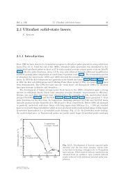
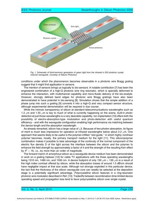
Fig. 1. Schematic of third-harmonic generation of green light from the infrared in SOI photonic crystal<br />
channel waveguide. Courtesy of Nature Photonics.<br />
conditions under which the phenomenon becomes observable in a photonic wire Bragg grating<br />
suggest that it might find application in sensors.<br />
The mention of sensors brings us logically to bio-sensors. A notable contribution [7] has been the<br />
engineered combination of a high-Q photonic wire ring resonator, which is specially deformed to<br />
enhance the interaction, with multichannel capability and micro-fluidic delivery of the bio-analyte.<br />
However, strongly defined band edges for photonic wire Bragg gratings have also been<br />
demonstrated to have potential in bio-sensing [8]. Simulation shows that the simple addition of a<br />
phase jump into such a grating [9] converts it into a high-Q and very compact sensor structure,<br />
although experimental demonstration will be required in due course.<br />
While the intrinsic transparency of silicon at standard telecommunications wavelengths such as<br />
1.3 m and 1.55 m is key to much of what is currently happening on the scene, built-in photodetection<br />
at just those wavelengths is a very desirable capability. Ion implantation [10] offers both the<br />
possibility of electro-absorption-type modulation and photo-detection with useful quantum<br />
efficiencyVand with the waveguide configuration enabling high performance via matching between<br />
the device length and the absorption wavelength.<br />
As already remarked, silicon has a large value of 3. Because of two-photon absorption, its figure<br />
of merit is much less impressive for operation at infrared wavelengths below about 2.2 m. One<br />
approach that seems likely to be useful is the polymer-infilled Bslot-guide,[ in which highly nonlinear<br />
polymer becomes, locally, the primary transport medium for the light [11]. This silicon/polymer<br />
combination makes it possible to take advantage of the continuity of the normal component of the<br />
electric flux density D of the light across the interface between the silicon and the polymer to<br />
enhance the field strength by approximately a factor of 4 and the strength of the resulting Kerr effect<br />
by 4 2 ¼ 16, i.e., by more than an order of magnitude.<br />
The forward march of amorphous silicon as a waveguide device medium has been demonstrated<br />
in work on a grating triplexer [12] for cable TV applications with the three operating wavelengths<br />
being 1310 nm, 1490 nm, and 1550 nm. A device footprint of only 150 m 130 m is a result of<br />
the high index contrast offered by silicon, while the absorption losses of around 1.5 dB/cm should<br />
have negligible impact at that size scale. Although not strongly exploited in this particular device,<br />
the fact that the thickness of the silicon waveguide core can readily be selected at the deposition<br />
stage is a potentially significant advantage. Polycrystalline silicon features in a ring-resonator<br />
photonic wire modulator described in Ref. [13]. Tradeoffs between recombination-time-limited device<br />
operating speed and propagation loss tend to favor polycrystalline silicon over single crystal.<br />
Vol. 2, No. 2, April 2010 Page 239<br />
Authorized licensed use limited to: <strong>ETH</strong> BIBLIOTHEK ZURICH. Downloaded on May 11,2010 at 11:24:39 UTC from IEEE Xplore. Restrictions apply.