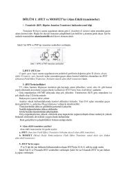
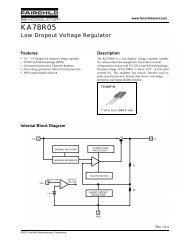
- Page 1 and 2: BU NOTLAR PROF. DR. AYTEN KUNTMAN T
- Page 3 and 4: 5.3.2. Gövde Parametresi(Taban kut
- Page 5 and 6: 1. GĐRĐŞ Tümdevre teknolojisi k
- Page 7 and 8: (b) (c) Şekil 2-1: Tümdevre üret
- Page 9 and 10: Şekil 3-1: Silisyum pul üzerinde
- Page 11 and 12: tanımlanır. Yasak band enerjisini
- Page 13 and 14: Şekil 3-5 : Fosfor katkılı Si kr
- Page 15 and 16: n i σ = q ( µ n N D + µ p ) yaz
- Page 17 and 18: Şekil 4-1 : Silisyumun borla difuz
- Page 19 and 20: olarak yazılır. Birimi Ω/€ ohm
- Page 21 and 22: Şekil 4-4 : Lokal oksitleme işlem
- Page 23 and 24: vardır. Bu tekniğin temelinde ele
- Page 25 and 26: Şekil 4-6: SiO 2 üzerinde pencere
- Page 27 and 28: Şekil 5-1: Kanal oluşturmalı N-M
- Page 29 and 30: a) b) 29
- Page 31 and 32: Đnce oksitin üzerine polisilisyum
- Page 33 and 34: Kanal Boyu: Kanalın kaynak-savak a
- Page 35 and 36: E g VDS (VGS − VTO ) − = 2 (5-7
- Page 37: Şekil 5-7: n-kanallı MOS tranzist
- Page 41 and 42: V T TO ( − 2Φ F + VSB − Φ F )
- Page 43 and 44: 5.3.4. MOS Tranzistörün Geçiş
- Page 45 and 46: Şekil 5-9: Kapasitelerin fiziksel
- Page 47 and 48: X d 2. εSi N A + N D = .( Φ 0 −
- Page 49 and 50: I sat n 2 D ( ) = β ( GS − T ) (
- Page 51 and 52: (b) Şekil 5-14: (a) test deveresi
- Page 53 and 54: kullanılır. Oluşturulan polisili
- Page 55 and 56: (a.2) 55
- Page 57 and 58: (c) 57
- Page 59 and 60: (e) 59
- Page 61 and 62: (g) Şekil 5-16: CMOS evirici tasar
- Page 63 and 64: Lambda-tabanlı serim tasarım kura
- Page 65 and 66: Şekil 6-1: MOSIS tasarım kurallar
- Page 67 and 68: Şekil 6-2 : Transistör için mini
- Page 69 and 70: Şekil 6-3 : nMOS ve pMOS arasında
- Page 71 and 72: Şekil 6-4: Standart NMOS evirici d
- Page 73 and 74: V L 2 ( −VTL ) = β / β D L V DD
- Page 75 and 76: 0). CMOS eviricinin Şekil 6.7’ d
- Page 77 and 78: 7.1. Jonksiyon Đzolasyonlu Bipolar
- Page 79 and 80: (c) (d) (e) (f) Şekil 7-1: Jonksiy
- Page 81 and 82: Şekil 7-2: Standart JIBT’ de kat
- Page 83 and 84: Şekil 7-3: npn transistörün dü
- Page 85 and 86: ψ 0 :Jonksiyona dışardan bir etk
- Page 87 and 88: Sebebi baz kontağının aktif baz
- Page 89 and 90:
Şekil 7-7: npn transistor için ba
- Page 91 and 92:
T:Bölgenin kalınlığı Bu modeli
- Page 94 and 95:
Şekil 7-11: Taban pnp yapısının
- Page 96 and 97:
R €= 1 qµ NT (7-19) Bağıntıs
- Page 98 and 99:
Şekil 7-14: npn ve pnp tranzistör
- Page 100 and 101:
• Ses ve Video Đle Đlgili devre
- Page 102 and 103:
Tranzistörlerin baz akımları ihm
- Page 104 and 105:
dosyalarından takip edilmek zorund
- Page 106 and 107:
.ends subname Örnek: .SUBCKT OPAMP
- Page 108 and 109:
COSC 17 23 10U IC=3V Yarıiletken k
- Page 110 and 111:
parametre Varsayılan değer Birim
- Page 112 and 113:
Tablo 8.7: Diyot model parametreler
- Page 114 and 115:
capacitance 20 VJE B-E built-in pot
- Page 116 and 117:
7 RD drain ohmic resistance 0.0 1.0
- Page 118 and 119:
Şekil: Alçak Geçiren Süzgeç Sp
- Page 120 and 121:
.DC VCE 0 10 .25 IB 0 10U 1U MOS tr
- Page 122 and 123:
Şekil: RLC devresinde direnç üze
- Page 124 and 125:
.NOISE V(5,3) V1 OCT 8 100 10kHz Si
- Page 126 and 127:
serimler bilgisayar programlarıyla
- Page 128 and 129:
.MODEL PMOD PMOS parametreleri kull
- Page 130 and 131:
Doğruluk Tablosu: F Çıkışı H
- Page 132 and 133:
NAND Kapısı Maskeleri: Şekil.1:C
- Page 134 and 135:
3.N+ difüzyonu 134
- Page 136 and 137:
5.Kontaklar 136
- Page 138 and 139:
Şekil.3:CMOS NOR Kapısı yapılar
- Page 140 and 141:
2.Geçit bölgesinin oluşturulmas
- Page 142 and 143:
4.P+ difüzyonu 142
- Page 144 and 145:
6. Metalizasyon ve bağlantılar T
- Page 146 and 147:
10. SORULAR 1. Bir tümdevre direnc
- Page 148 and 149:
B A A ’ Active Polysilic on Metal
- Page 150 and 151:
Vgs=3V Vgs=2V Vgs=1V Şekil. 2: PMO
- Page 152 and 153:
15. Bir CMOS eviricide K p =µ p C
- Page 154 and 155:
derinliği 2 µ m olduğuna göre t
- Page 156 and 157:
direnci 50 ohm olduğuna göre böl
- Page 158:
7. P.Antapnetti, Gossobrio, Semicon