PLASMA IMMERSION ION IMPLANTATION AS AN ALTERNATIVE ...
PLASMA IMMERSION ION IMPLANTATION AS AN ALTERNATIVE ...
PLASMA IMMERSION ION IMPLANTATION AS AN ALTERNATIVE ...

Create successful ePaper yourself
Turn your PDF publications into a flip-book with our unique Google optimized e-Paper software.
<strong>PL<strong>AS</strong>MA</strong> <strong>IMMERS<strong>ION</strong></strong> <strong>ION</strong> IMPL<strong>AN</strong>TAT<strong>ION</strong> <strong>AS</strong> <strong>AN</strong> <strong>ALTERNATIVE</strong> TO DIFFUS<strong>ION</strong> <strong>AN</strong>D BEAM-LINE<br />
IMPL<strong>AN</strong>TAT<strong>ION</strong> FOR CREATING PHOSPHORUS DOPED EMITTERS <strong>AN</strong>D SELECTIVE EMITTERS<br />
A. Lawerenz 1 *, K. Neckermann 1 , G. Andrä 2<br />
1 CiS Forschungsinstitut für Mikrosensorik und Photovoltaik GmbH, Konrad-Zuse-Str. 14,99099 Erfurt, Germany<br />
2 Institute of Photonic Technology, Albert-Einstein-Str. 9, 07745 Jena, Germany<br />
*corresponding author: alawerenz@cismst.de; Tel: +49 - 361 - 663 1212, Fax: +49 - 361 - 663 1413<br />
ABSTRACT: The plasma immersion ion implantation (PIII) can be used to implant phosphorus ions into the silicon<br />
surface. Therefore it is a possible alternative to other doping techniques as phosphorus diffusion or beam<br />
implantation. For a successful implantation into a solar cell processing line, some obstacles that are dealt with in this<br />
contribution have to be overcome. We are investigating possible paths for the activation and annealing step that is<br />
necessary for getting sufficient sheet resistances and we are correlating processing parameters to solar cell parameters<br />
as doping profiles, emitter saturation currents and solar cell efficiencies, both for mono- and multicrystalline wafers.<br />
Furthermore we are investigating the possibility of a laser assisted selective emitter process.<br />
Keywords: Implantation, Selective Emitter, Crystalline Silicon Solar Cells<br />
1 INTRODUCT<strong>ION</strong><br />
In the last three years, ion beam line implantation has<br />
shown its potential to replace the diffusion process by<br />
implanting phosphorus and boron atoms into solar wafers<br />
and to be integrated into the solar cell production [Gupta<br />
2010, Yelundur 2011]. In our contribution we are<br />
investigating whether an alternative implantation<br />
technique – plasma immersion ion implantation (PIII or<br />
simply plasma implantation) – is also feasible for the<br />
solar cell processing. Compared to the established<br />
diffusion technique, plasma implantation has the<br />
following advantages. It is a single-side process (making<br />
the removal or overcompensation of back-side doping<br />
unnecessary), there is no phosphorus and boron silicate<br />
glass formation (making its removal also unnecessary)<br />
and it enables a conformal doping, which makes it<br />
suitable for heavily textured surfaces as acid etched<br />
multicrystalline silicon. On the other hand, implantation<br />
causes a damage in the implanted region near to the<br />
surface, which has to be cured, and the implanted dopants<br />
have to be activated. This activation and annealing has to<br />
be done at elevated temperatures.<br />
Compared to the beam line implantation, large<br />
surface areas can be faster implanted and the already<br />
mentioned conformal doping might be easier, but the<br />
energy distribution of the plasma excited implantation<br />
ions is much broader. The latter effect is for the<br />
application of solar cells still tolerable.<br />
Until now, there are only very few publications<br />
dealing with plasma implantated solar cells [3]. Therefore<br />
it is not surprising that plasma implanted (p-type) solar<br />
cells could not reach efficiencies comparable to POCl 3<br />
diffused solar cells.<br />
Our contribution focuses on phosphorus plasma<br />
implantation parameters, the feasibility of different<br />
activation and annealing steps and the possibility of<br />
structuring implanted regions by a laser assisted<br />
activation for creating selective emitters.<br />
2 EXPERIMENTAL<br />
2.1 Wafer material<br />
For processing solar cells, solar grade silicon wafers<br />
have been used (CZ, 3 - 6 Ωcm, 156 mm edge length,<br />
alkaline textured and multicrystalline, 1.5 Ωcm, 156 mm<br />
edge length, acid etched). For lifetime measurements<br />
(including the determination of interstitial iron content)<br />
the same sort of wafers has been used, but after shiny<br />
etch treatment to obtain smooth surfaces. For the<br />
determination of the emitter saturation current, high<br />
resistance wafers (10 - 17 Ωcm) have been used, again<br />
after a shiny etch treatment.<br />
2.2 Plasma implantation<br />
Plasma implantation was carried out at Ion Beam<br />
Services (Peynier, France) and at Helmholtz-Zentrum<br />
Dresden-Rossendorf e. V. (Dresden, Germany). Because<br />
of the large scattering of the energy of the ions, a precise<br />
number for the energies cannot be given. Doses varied<br />
from 1.5 to 10 · 10 15 at/cm 2 .<br />
2.3 Activation and annealing<br />
The activation and annealing step (short: activation),<br />
necessary for activating the implanted phosphorus atoms<br />
and curing the implantation damage, was carried out by<br />
different methods (s. Table I and II). The laser used was<br />
an excimer laser with a top-hat profile and an<br />
illumination area of 6 × 6 cm 2 . The flash lamp annealing<br />
took place at and was carried out by Helmholtz-Zentrum<br />
Dresden-Rossendorf e. V. (Dresden, Germany).<br />
Table I: Furnaces applied for the activation step<br />
Furnace Temperture Duration<br />
range (°C) range<br />
Walking string inline 880 - 950 20 - 50 min<br />
furnace (Centrotherm)<br />
Quarz tube furnace 950 - 1050 5 - 30 min<br />
(Inotherm)<br />
RTP furnace (Unitemp) 800 - 900 2 - 10 min<br />
Sintering furnace 850 1 - 5 s<br />
(Centrotherm)<br />
Flash lamp annealing 1100 - 1200 20 ms<br />
Table II: Laser applied for the activation step<br />
Laser Wavelength Pulse Pulse<br />
λ (nm) duration repetition<br />
Excimer laser 248 25 ns 50 Hz
Solar cells were processed using the standard<br />
processing line of the CiS Forschungsinstitut.<br />
2.4 Measuring methods<br />
Sheet resistances have been measured by a four point<br />
probe (Napson RT-70 tester), and sheet resistance<br />
mappings of the implanted and annealed wafers have<br />
been carried out by two methods (SHR, “sheet<br />
resistance” with a measuring head on a semilab WT2000<br />
and SRI, “sheet resistance imaging” with a<br />
Thermosensorik infrared camera system).<br />
Carrier lifetime measurements were carried out on<br />
samples whose emitter has been etched off past the<br />
implantation and activation with a Semilab WT2000 tool<br />
and a Sinton Consulting WCT-100. The latter has been<br />
also used (on the same type of samples) for determining<br />
the interstitial iron content, the emitter saturation currents<br />
and for Illumination V oc-characteristics (“SunsVoc”).<br />
Illumination V oc measurements were achieved on<br />
samples having a screen printed aluminum rear side and<br />
no metallisation at the front.<br />
Phosphorus depth profiles were determined with a<br />
Cameca sector field secondary ion mass spectrometre<br />
(SIMS).<br />
3 <strong>AN</strong>NEALING <strong>AN</strong>D ACTIVAT<strong>ION</strong><br />
Because a drive-in of impurities at high temperatures<br />
applied at the activation step has to be avoided, the wafer<br />
surface has to be cleaned before the activation. A<br />
standard clean like the RCA clean is not suitable in our<br />
case, because it causes too large a removal of the surface<br />
and thus a significant increase of the sheet resistance after<br />
the activation step. Therefore a reduced RCA process<br />
consisting of the SC2 step followed by an HF dip has<br />
been used for the activation in the walking string inline<br />
furnace.<br />
3.1 Sheet resistance<br />
With increasing annealing times, more and more<br />
phosphorus atoms are becoming activated and at the<br />
same time are diffusing deeper into the silicon bulk. The<br />
latter causes a decrease in the concentration of<br />
phosphorus atoms and therefore to an increase in the<br />
carrier mobility. Both effects (activation and diffusion)<br />
lead to a decrease in the sheet resistance with increasing<br />
annealing times t. An example is shown in Fig. 1 for an<br />
implantation with a bias voltage of 8 kV and a dosis of 5 ·<br />
10 15 at/cm 2 and an activation in an inline diffusion<br />
furnace (temperature: 880 °C). The fast decrease of the<br />
sheet resistance (t ≤ 10 - 20 min) is attributed mainly to<br />
the activation, and the slow decrease (t ≥ 20 min) to the<br />
diffusion of the phosphorus atoms into the bulk.<br />
All relevant sheet resistances R sh (30 Ω/sq < R sh <<br />
120 Ω/sq) can easily be obtained for monocrystalline<br />
wafers by a sufficient dose and activation temperature<br />
(for example for R sh = 30 Ω/sq an implantation of 5 keV,<br />
10 16 at/cm 2 and an activation of 1000 °C, 10 min is<br />
sufficient). It is noteworthy that the activation for plasma<br />
implanted samples is much shorter than the diffusion<br />
time for phosphorus diffused samples. This holds also for<br />
RTP processes, where 10 min at 600 °C and 2 min at<br />
900 °C in N 2-atmosphere are enough to gain a sheet<br />
resistance of 50 Ω/sq (again with the same implantation<br />
parameters). Nevertheless the activation in a sintering<br />
furnace with parameters sufficient for the contact<br />
formation of screen printed metals is by far not sufficient<br />
to reach reasonable sheet resistances. Therefore an<br />
explicit activation step for the processing of standardtype<br />
solar cells cannot be avoided.<br />
For multicrystalline wafers, it is remarkable that for<br />
the same implantation an activation with a higher<br />
temperature or duration is needed to reach the same sheet<br />
resistances as for the monocrystalline samples.<br />
Homogeneities of the sheet resistance for the<br />
implanted and activated samples are sufficient for the<br />
processing of solar cells. An example is shown in Fig. 2<br />
for the same implantation parameters and the same<br />
furnace used (880 °C, 20 min). A sheet resistance of 53<br />
± 2 Ω/sq measured with a four point probe at nine points<br />
has been obtained (standard deviation of 4 %). (The high<br />
sheet resistance values at the edge of the wafer (red<br />
colour) in Fig. 2 are an artefact of the SHR measuring<br />
technique due to the fact that the current path is inhibited<br />
at the wafer edges.)<br />
Sheet resistance [Ω/sq]<br />
90<br />
80<br />
70<br />
60<br />
50<br />
40<br />
0 20 40 60 80 100<br />
Annealing time [min]<br />
Figure 1: Sheet resistances after activation using an<br />
inline diffusion furnace<br />
Figure 2: Sheet resistance (SHR) image of a walking<br />
string inline furnace annealed wafer<br />
3.2 Phosphorus depth profiles<br />
There is a good correlation between implantation and<br />
activation parameters and the phosphorus depth profiles<br />
measured with SIMS. After implantation (and before
activation) an almost exponential depth profile can be<br />
observed with a penetration depth (where the P<br />
concentration decreases by a factor of e -1 ) of 7 to 8 nm<br />
(dependent on the ion energy) and a surface<br />
concentration of 5 to 50 · 10 21 at/cm 3 resulting in an<br />
overall P content that is in good agreement with the<br />
implanted dose.<br />
After activation, depth profiles of the overall and the<br />
activated phosphorus concentration have been measured<br />
for a quartz tube furnace and an excimer laser activation<br />
with SIMS and ECV (Electrochemical Capacitance<br />
Voltage Profiling), respectively (s. Fig. 3). The observed<br />
low differences in both profiles are indicating that at least<br />
almost all phosphorus atoms are activated after these two<br />
activation methods (implantation: 5 keV, 10 16 at/cm 2 ,<br />
quartz tube furnace: 1000 °C, 10 min).<br />
For a quartz tube furnace (and similarly for the<br />
walking string inline furnace), SIMS profiles look<br />
different from those that are known from POCl 3 or sprayon<br />
inline diffusion processes (cf. eg. [4]). Especially the<br />
kink that is found in diffused P samples (at about 2 · 10 19<br />
cm -3 ), cannot be found in our cases. One reason for this<br />
might be the lower phosphorus surface concentration.<br />
Similarly to diffused samples, a hunch in the profile can<br />
be detected at 2 - 5 · 10 18 cm -3 indicating the same<br />
diffusion process that is dominated by interaction with<br />
self-interstitials.<br />
Profiles obtained from laser activated samples can<br />
quite be varying, depending on the exact laser parameters<br />
that are responsible for the fact whether the silicon<br />
surface is molten or just heated. In our case, the surface is<br />
molten (albeit a complete mixing of the recrystallised<br />
silicon not reached for one laser pulse), leading to a<br />
profile that shows the same characteristics as the quartz<br />
tube furnace process, but on a much smaller scale (a<br />
concentration of 5 · 10 17 cm -3 is reached at a depth of ca.<br />
250 nm compared to 1000 nm for the quartz tube furnace<br />
activation). This might be due to the much lower laser<br />
impact time (25 ns).<br />
4 ELECTRICAL CHARACTERISAT<strong>ION</strong><br />
4.1 Carrier lifetime<br />
Carrier lifetimes were measured on samples whose<br />
emitter has been etched off after the implantation and<br />
activation and which were passivated afterwards by<br />
silicon nitride coatings. Therefore the quoted<br />
(“effective”) lifetimes are upper limits for the “true” bulk<br />
lifetime. In our experiments, no influence of the<br />
implantation parameters can be ascertained - in contrast<br />
to the activation parameters. There is a tendency, that (in<br />
the case of RTP furnace) higher temperatures yield lower<br />
lifetimes which is possibly caused by some<br />
contamination. For activation steps other than hightemperature-RTP,<br />
effective lifetimes vary from 200 µs to<br />
800 µs.<br />
P Concentration [at./cm³]<br />
P Concentration [at./cm³]<br />
10 21<br />
10 20<br />
10 19<br />
10 18<br />
10 17<br />
10 16<br />
quartz tube furnace<br />
SIMS<br />
ECV<br />
10<br />
0,0 0,5 1,0 1,5<br />
15<br />
10 21<br />
10 20<br />
10 19<br />
10 18<br />
10 17<br />
10 16<br />
Depth [µm]<br />
10<br />
0,0 0,1 0,2 0,3 0,4<br />
15<br />
Depth [µm]<br />
excimer laser<br />
SIMS<br />
ECV<br />
Figure 3: SIMS and ECV depth profiles after activation<br />
for quartz tube furnace and excimer laser<br />
The WCT-100 tool has been used to determine the<br />
interstitial iron (Fe i) content (by measuring lifetimes<br />
before and after a light soaking of the passivated<br />
samples). After the activation, we observe partly an<br />
increase and partly a decrease of the interstitial iron<br />
content in comparison to the Fe i content after the<br />
implantation. A conclusion, whether a gettering effect or<br />
contamination or an internal regrouping of iron atoms<br />
(from the interstitial/boron pair state to iron containing<br />
precipitates and vice versa) dominates, is not yet<br />
possible.<br />
4.2 Emitter saturation current<br />
The same set of samples used for illustrating the<br />
dependence of the sheet resistance R sh on the activation<br />
time (Fig. 1) has been used for measuring the emitter<br />
saturation current density (J 0e) (Fig. 4). Quite often, a<br />
monotonic decrease of J 0e for increasing sheet resistances<br />
is measured for phosphorus diffused samples. In our case,<br />
such a decrease is observed only for sheet resistances<br />
above 55 Ω/sq. The reason for the increase in J 0e for 45<br />
Ω/sq < R sh < 55 Ω/sq is not known yet. The absolute<br />
values we obtained are still somewhat high and do not<br />
suffice for the processing of high efficiency solar cells.
J 0E [fA/cm²]<br />
300<br />
250<br />
200<br />
150<br />
40 45 50 55 60 65 70 75 80 85<br />
Sheet resistance [Ω/sq]<br />
Figure 4: Emitter saturation current density in<br />
dependence of the sheet resistance<br />
4.3 Illumination V oc<br />
Illumination V oc is a means to assess solar cell<br />
parameters as pseudo fill factor (pseudo FF), pseudo<br />
efficiency (pseudo η) and open circuit voltage V oc before<br />
the final metallisation (in our case a screen printed front<br />
metallisation). For different activation steps, the best<br />
illumination V oc values are listed in Table III (the<br />
combination of RTP and laser has been used for the<br />
activation of selective emitter structures, s. below). The<br />
relatively high pseudo FF are ensuring that shunting<br />
problems are not relevant and cannot be responsible for<br />
the low open circuit voltages. We assume the low V oc<br />
values are caused by a high recombination in the bulk<br />
and emitter region (hence the high j 01 and j 02 values).<br />
Table III: V oc and pseudo cell parameters, measured<br />
with illumination V oc<br />
Activation inline RTP laser RTP +<br />
furnace laser<br />
pseudo η [%] 13.5 13.0 12.9 13.1<br />
V OC [mV] 580 550 570 554<br />
pseudo FF [%] 80 81 76 79<br />
j 01 [pA/cm²] 51 18 52 8<br />
j 02 [nA/cm²] 79 67 143 100<br />
4.4 Solar cells<br />
For different activation steps and both for CZ and<br />
multicrystalline (mc) wafers, the best solar cell values are<br />
listed in Table IV. In comparison to the illumination V oc<br />
values, it is remarkable that V oc and (pseudo) FF values<br />
are decreased. One possible reason for this (high series<br />
resistances, R ser) can be excluded for most cases because<br />
R ser values are tolerable (< 1 Ωcm 2 , not shown here).<br />
Similar to illumination V oc, we assume that a high carrier<br />
recombination is responsible for the rather bad solar cell<br />
characteristics. This is confirmed by spectrally resolved<br />
light beam induced current (SR-LBIC) mappings,<br />
showing effective diffusion length values below 100 µm<br />
(also not shown here).<br />
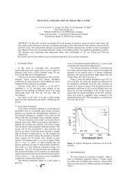
IQE measurements show that the emitter region λ <<br />
400 nm is reasonably well in contrast to the low values<br />
for λ > 600 nm (Fig. 5). This again is a hint for a material<br />
degradation.<br />
Table IV: Results of plasma implanted solar cells<br />
RTP inline quartz tube<br />
furnace furnace<br />
mc solar cells<br />
JSC [mA/cm²] 31 30<br />
VOC [mV] 561 564<br />
FF [%] 72 74<br />
η [%] 12.3 12.3<br />
CZ solar cells<br />
J SC [mA/cm²] 29 26 30<br />
V OC [mV] 544 551 554<br />
FF [%] 76 60 77<br />
η [%] 12.2 8.8 13.0<br />
EQE<br />
1,0<br />
0,8<br />
0,6<br />
0,4<br />
0,2<br />
0,0<br />
400 600 800 1000 1200<br />
wave length [nm]<br />
RTP<br />
quartz<br />
tube<br />
Figure 5: Internal quantum efficiency for two CZ solar<br />
cells with a plasma implanted emitter annealed using<br />
RTP or quartz tube furnace<br />
5 SELECTIVE EMITTER<br />
5.1 Laser treatment<br />
For processing selective emitter structures, the areas<br />
between front side fingers (‘high resistivity areas’) are<br />
activated by annealing the implanted wafers in an RTP<br />
furnace. The following parameters turned out to be best<br />
suited to process the high resistivity areas: implantation<br />
(3 kV, 1 x 10 15 at / cm 2 ) and RTP activation (600 °C,<br />
10 min, obtaining R sh = 120 Ω / sq). The low resistivity<br />
areas below the metallisation fingers were illuminated by<br />
an excimer laser (details see section 2.3). Fig. 6 illustrates<br />
the impact the laser has on the silicon surface. A slight<br />
rounding of the otherwise sharp-edged surface texture is<br />
observed.<br />
Figure 6: SEM image of the acid etched silicon surface<br />
of mc wafer before (left) and after (right) laser treatment<br />
5.2 Results<br />
Because the high resistivity area is activated by a low<br />
temperature process for only a short time, there remains<br />
the possibility to decrease further the resistivity locally
y a laser. This is visualised by SRI (Fig. 7), where the<br />
red colour indicates a higher emittivity (and thus a higher<br />
conductivity) of the silicon than the yellow colour. In<br />
these low resistance areas a sheet resistance of 36 Ωcm<br />
could be achieved.<br />
Figure 7: Sheet resistance imaging (SRI) of selective<br />
emitter (distance between fingers ca. 300 µm).<br />
6 CONCLUS<strong>ION</strong><br />
The reason why solar cells with plasma implanted<br />
phosphorus emitters lack the efficiencies which are<br />
standard to the phosphorus diffused emitter solar cells is<br />
not yet understood. Until now it is only an assumption<br />
that there is a degradation due to a reduction of the<br />
effective lifetime during solar cell processing.<br />
Contamination with iron is one candidate for this.<br />
Although for low phosphorus concentrations a similar<br />
depth profile to phosphorus diffused emitters can be<br />
obtained, it is improbable that an effective phosphorus<br />
diffusion gettering takes place during processing of<br />
plasma implanted solar cells. Therefore the processing of<br />
this kind of solar cells affords a special awareness in<br />
respect to wafer qualities, clean process surroundings and<br />
the interaction of impurities during processes.<br />
On the other hand, we observed shunting or<br />
contacting (series resistance) problems only in very few<br />
cases. Homogeneity of emitters and the screen printing of<br />
a silver based metallisation even for low phosphorus<br />
surface concentrations does not seem a problem. The heat<br />
necessary for the activation is by far not as large as the<br />
heat needed for diffusion processes where the phosphorus<br />
has to be driven into the silicon bulk from a surface<br />
coating. Therefore we consider the plasma implantation<br />
method still a very promising method for producing<br />
commercially viable solar cells.<br />
6 ACKNOWLEDGEMENTS<br />
The autors like to thank Christian Schmiga and<br />
Michael Rauer from Fraunhofer ISE, Freiburg, Germany<br />
for providing the ECV measurements. The authors thank<br />
their colleagues from Ion Beam Services (Yannick<br />
Cizeron, Hasnaa Etienne, Thomas Michel) and at<br />
Helmholtz-Zentrum Dresden-Rossendorf (Andreas<br />
Kolitsch, Wolfgang Skorupa, Johannes von Borany, S.<br />
Prucnal) for conducting the plasma implantation and the<br />
flash lamp annealing and also for fruitful discussions.<br />
The financial support by the German Bundesministerium<br />
für Wirtschaft und Technologie (BMWi) is gratefully<br />
acknowledged for funding the project Flaem under the<br />
contract number VF 090004.<br />
7 REFERENCES<br />
[1] A. Gupta et al.: High efficiency selective emitter cells<br />
using in-situ patterned ion implantation; 25 th EU PVSEC,<br />
2010, p. 1158<br />
[2] V. Yelundur et al: First implementation of ion<br />
implantation to produce commercial silicon solar cells,<br />
26 th EU PVSEC, 2011, p. 831<br />
[3] Á. Németh, I. Pintér, Z. Lábadi, A. Tóth, S. Püspöki:<br />
Study of Crystal Defects in Plasma Doped Silicon Solar<br />
Cells, 21 st EU PVSEC, 2006, 1400 – 1403<br />
[4] A. Bentzen, J.S. Christensen, B.G. Svensson, and A.<br />
Holt: Understanding phosphorus emitter diffusion in<br />
silicon solar cell processing; 21 st EPVSEC, 2006, p. 1388