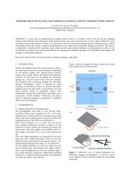
LOCAL STRUCTURING OF DIELECTRIC LAYERS ON SILICON ...
LOCAL STRUCTURING OF DIELECTRIC LAYERS ON SILICON ...
LOCAL STRUCTURING OF DIELECTRIC LAYERS ON SILICON ...

You also want an ePaper? Increase the reach of your titles
YUMPU automatically turns print PDFs into web optimized ePapers that Google loves.
<strong>LOCAL</strong> <strong>STRUCTURING</strong> <strong>OF</strong> <strong>DIELECTRIC</strong> <strong>LAYERS</strong> <strong>ON</strong> SILIC<strong>ON</strong> FOR IMPROVED SOLAR CELL<br />
METALLIZATI<strong>ON</strong><br />
K. Neckermann 1 , S. A. G. D. Correia 2 , G. Andrä 3 , M. Bähr 1 , J. Lossen 2 , E. Ose 3 , L. Redlich 3 , I. Köhler 4 , H. Metzner 1<br />
1 SolarZentrum Erfurt, CiS Institut für Mikrosensorik GmbH, Konrad-Zuse-Str. 14, 99099 Erfurt, Germany,<br />
Phone: +49 - 361 - 663 12 14, Fax: +49 - 361 - 663 14 13, E-mail: kneckermann@cismst.de<br />
2 ersol Solar Energy AG, Wilhelm-Wolff-Str. 23, 99099 Erfurt, Germany<br />
3 Institut für Physikalische Hochtechnologie e. V., Albert-Einstein-Str. 9, 07745 Jena, Germany<br />
4 Merck KGaA, P.O. Box, 64271 Darmstadt, Germany<br />
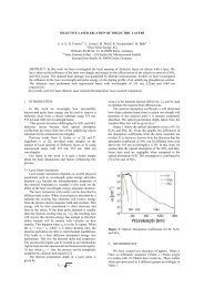
ABSTRACT: Using different types of nanosecond lasers with wavelengths in the range from 248 to 1064 nm and a<br />
femtosecond (fs) laser with λ = 785 nm, dielectric SiN x or SiO x layers on silicon wafers were opened locally to form<br />
diffusion and metallization masks. The wafers were all Cz-grown single-crystalline material and were either smooth, i.e.<br />
shiny etched, or textured and had a phosphorus-doped emitter or not. For all laser types, the laser parameters which were<br />
necessary and sufficient to open the dielectric layers were determined as optimal parameters. Additionally, screenprinted<br />
etching pastes were employed to open the dielectric layers in parallel experiments. The opened structures were<br />
characterized microscopically and by means of effective minority carrier lifetime measurements. The effects of the<br />
utilized laser parameters on surface structure and carrier lifetime are discussed. Secondary ion mass spectroscopy reveals<br />
the effects of the different laser irradiations on the phosphorus doping profile. SunsVoc measurements confirm the<br />
capability of the investigated process steps in solar-cell processing.<br />
Keywords: laser processing, silicon nitride, silicon oxide<br />
1 INTRODUCTI<strong>ON</strong><br />
The efficiency of crystalline silicon solar cells out of<br />
the standard industrial process is limited due to<br />
restrictions imposed by the generally employed screenprinting<br />
process for front and back-side metallization [1].<br />
On the front side, the metallization pastes have to be<br />
optimized simultaneously for the pervasion of the<br />
standard dielectric SiN x layer, a good ohmic contact to<br />
the emitter, and a low specific resistance. That is why<br />
screen printing on the front side is, in general, only<br />
applicable to emitters with sheet resistances beneath a<br />
certain level. Moreover, the comparatively high series<br />
resistances produced by the front-side metallization<br />
reduce the fill factor and thus the efficiency of the<br />
processed cells.<br />
Therefore, some effort has been devoted to the<br />
investigation of alternative metallization procedures<br />
which are compatible to low-cost industrial mass<br />
production [2]. Among these, laser processes offer some<br />
advantages when employed to open defined local<br />
structures in the anti-reflection coating on the front of the<br />
cell. These local structures are then susceptible for<br />
promising metallization processes including wet<br />
chemical processes and also screen printing with lowresistivity<br />
pastes which can be processed at<br />
comparatively low temperatures. On the other hand, laser<br />
processing is well-known to be capable of introducing<br />
material modifications into silicon wafers including<br />
lifetime limiting defects and internal stress [3]. Hence,<br />
before these alternative metallization concepts can enter<br />
into production their benefits have to be shown on a<br />
laboratory scale first.<br />
In this paper, we open locally different types of<br />
dielectric layers, either SiN x or SiO x , by different types<br />
of lasers in order to shed light on the interplay of laser<br />
beams and material effects as a function of laser<br />
parameters such as wavelength, energy fluence, pulse<br />
length and pulse repetition time. The SiN x layers are part<br />
of the industrial standard cell, while SiO x films play<br />
important roles in various high-efficiency concepts. To<br />
compare with the laser processes, a screen-printed<br />
etching paste is used for a local opening of the dielectric<br />
layers.<br />
The ablation of the dielectric layers SiN x and SiO x<br />
without damaging the underlying silicon surface using a<br />
nanosecond laser is difficult because of the low<br />
absorption coefficient of SiN x and SiO x in comparison to<br />
silicon [4]. Thus, it is very important to choose adequate<br />
wavelengths, for which absorption in the dielectric layer<br />
takes place. As a consequence a laser wavelength of<br />
λ < 350 nm is required for light absorption within the<br />
SiN x layer. Still lower wavelengths are needed for<br />
absorption within SiO x . By using very small pulse<br />
duration in the femtosecond range non-linear effects [5]<br />
in the absorption process result in ablation of material<br />
nearly without heat transfer.<br />
2 EXPERIMENTAL DETAILS<br />
In the present experiments, different lasers or an<br />
etching paste were employed to open dielectric SiN x or<br />
SiO x layers on Cz-Si wafers. The latter had been<br />
processed according to the pathways of the reaction<br />
scheme which is depicted in figure 1. Therefore we used<br />
an industrial standard diffusion process (ρ sh = 47 Ω/sq),<br />
an industrial standard PECVD SiN x of about 80 nm and a<br />
APCVD SiO x of 100 nm thickness.<br />
Figure 1: Scheme of processing of the used wafers.
The laser experiments included the following<br />
features:<br />
• Nd:YAG laser, λ = 1064 nm<br />
• Nd:YAG laser, λ = 532 and 355 nm<br />
• Excimer laser with λ = 248 nm<br />
• Ti:sapphir laser with λ = 785 nm<br />
The Nd:YAG lasers and the Excimer laser have pulse<br />
durations in nanosecond range whereas the Ti:sapphire is<br />
a femtosecond laser.<br />
The parameters for a complete opening of the<br />
dielectric layers were determined for each laser (optimal<br />
parameters). To this end, the fluences of the Nd:YAG<br />
lasers and the femtosecond laser were varied. For the<br />
excimer laser, the number of pulses at a constant fluence<br />
of 580 mJ/cm² was changed.<br />
The etching paste was Solar Etch BE 01 of Merck<br />
which was printed by means of a common screen printer.<br />
The nominal finger width of the screen was chosen to be<br />
80-85 µm. The etching paste was activated by a heat<br />
treatment at 350°C for 90 s and was finally removed by<br />
0.1 % KOH at 40°C in an ultrasonic bath for 90 s.<br />
Figure 2: SEM images at the textured silicon surface<br />
after laser opening of the SiN x layer with different lasers<br />
using the optimal parameters: a) λ = 1064 nm, b)<br />
λ = 532 nm, c) λ = 355 nm and d) femtosecond laser with<br />
λ = 785 nm.<br />
3 RESULTS AND DISCUSSI<strong>ON</strong><br />
3.1 Optical characterizations<br />
As a first step, the laser fluence in combination with<br />
the other laser parameters, which are necessary and<br />
sufficient to remove locally the dielectric SiN x or SiO x<br />
layer were determined. These fluences range from 0.03 to<br />
7.75 J/cm² for the Nd:YAG lasers. The parameters, for<br />
which the dielectric layer was completely opened while<br />
damaging the Si surface as little as possible, will be<br />
referred to as "optimal parameters". The fluences of the<br />
optimal parameters are between 0.8 and 0.1 J/cm².<br />
Figure 2 shows examples of SEM images of areas of<br />
textured wafers, where the SiN x layer has been removed<br />
using the optimal parameters. For the longest wavelength<br />
of 1064 nm, the image indicates a complete surface<br />
melting (a), while for the shorter wavelengths of 532 and<br />
355 nm the tops of the pyramids only show signs of<br />
melting, (b) and (c), respectively. These observations<br />
were made after irradiation with a Nd:YAG laser,<br />
whereas the short pulse femtosecond laser (785 nm) in<br />
figure 2 (d) apparently did not induce any surface<br />
modifications.<br />
In the SEM image of Fig. 3 (a), which shows laser<br />
irradiated and non-irradiated areas, we are confronted<br />
with a less pronounced surface texture below a SiO x<br />
layer, the removal of which is clearly accompanied by a<br />
complete surface melting (Nd:YAG, 1064 nm).<br />
Proceeding to the shorter wavelength of 532 nm, the<br />
surface melting appears to be less complete (b), while<br />
finally, at 355 nm (c) the topmost Si layer only was<br />
melted and so a somewhat smoothed texture appears.<br />
Using fluences above the optimal one at a constant<br />
wavelength, the silicon surface is melted more and more.<br />
Figure 3: SEM images at the textured silicon surface<br />
after laser opening of the SiO x layer with different<br />
Nd:YAG lasers using the optimal parameters: a)<br />
λ = 1064 nm, b) λ = 532 nm and c) λ = 355 nm.<br />
Surface melting is avoided when etching pastes are<br />
used instead of lasers. Fig. 4 shows images taken with an<br />
optical microscope which demonstrate the precise local<br />
removal of a SiN x layer by the etching paste on a smooth<br />
(a) and a textured surface (b). The measured line width is<br />
about 105 µm for the shiny-etched surface and 125 µm<br />
for the textured surface. At the edges of the lines thinner<br />
layer thickness is observed due to sloping of the paste.<br />
The same results were observed after local removing of<br />
SiO x layers. Furthermore, comparable geometries can be<br />
obtained with laser processing (not shown).
Figure 4: Optical microscopy pictures of local structured<br />
SiN x layers on a shiny etched (a) and a textured (b)<br />
surface.<br />
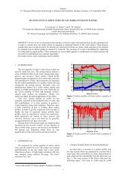
3.2 Lifetime measurements<br />
Minority carrier lifetime measurements using the<br />
MWPCD (microwave-detected photoconductance decay)<br />
were carried out in order to look for the effects of the<br />
local opening of the dielectric films on the electronic<br />
quality of the underlying bulk material. These<br />
measurements were done on smooth shiny-etched wafers<br />
without emitter, after the remaining parts of the dielectric<br />
layers had been removed in HF and after subsequent<br />
surface passivation using iodine ethanol solution. Fig. 5<br />
(left) shows lifetime mappings of a wafer piece with<br />
three columns of laser-opened stripes which are clearly<br />
visible as stripes of low lifetime. The columns<br />
correspond to the indicated laser wavelengths (Nd:YAG)<br />
while the laser fluence is decreasing from top to bottom.<br />
The stripes which relate to the optimal fluences are<br />
encircled. Fig. 5 (right) shows the lifetime mapping of a<br />
wafer piece which had had four quadratic windows in the<br />
dielectric layer each opened with an excimer laser at<br />
different pulse numbers (between 10 and 500) with<br />
constant energy per pulse. Obviously, the number of<br />
pulses does not very much affect the lifetime which is<br />
lowered to a few micro-seconds in all four cases. The<br />
encircled window corresponds to the critical number of<br />
pulses which is 50.<br />
Figure 5: Lifetime measurements after laser opening of<br />
the SiN x layer using the different Nd:YAG lasers<br />
(λ = 355-1064 nm) and the Excimer laser (λ = 248 nm)<br />
after iodine ethanol passivation.<br />
Fig. 6 shows analogous examples of lifetime<br />
mappings of wafer pieces on which windows in the<br />
covering SiN x (left) or SiO x (right) layers had been<br />
produced by means of fs-laser irradiation. In these<br />
examples, the lifetime is - as in the examples of Fig. 5 -<br />
also reduced to a few micro-seconds in the laser-treated<br />
areas although these wafer pieces yielded a much higher<br />
lifetime for the non-irradiated areas due to better quality<br />
of the starting material.<br />
Figure 6: Lifetime measurements on two wafer pieces<br />
where the dielectric layers SiN x (left) and SiO x (right)<br />
were locally opened with the femtosecond laser. The<br />
structures lasered with the optimal parameters are<br />
encircled.<br />
In contrast to the laser treated wafers, the opening of<br />
the dielectric layers with an etching paste does not at all<br />
affect the lifetime. This is illustrated in Fig. 7, which<br />
shows a sketch of the printed test structure (left) and the<br />
corresponding lifetime mapping of the wafer piece. In<br />
this case, a SiN x film had been opened. For SiO x layer<br />
opening, also effects on carrier lifetime do not occur.<br />
Figure 7: Sketch of the opened structures using the<br />
etching paste (left) and the lifetime mapping of the<br />
structured wafer after iodine ethanol passivation.<br />
3.3 SIMS analyses<br />
As mentioned above, an important possible<br />
application of laser-opened local structures in dielectric<br />
layers will be a modification or complete substitution of<br />
screen printed front contacts. Therefore, the reaction of<br />
the phosphorous doped emitter to the laser treatment will<br />
be of major importance. Fig. 8 shows a SIMS (secondary<br />
ion mass spectroscopy) measurement of the phosphorus<br />
depth profile of a standard industrial emitter which is<br />
termed "starting profile" and the profiles which result<br />
from this starting profile due to the laser irradiation with<br />
different lasers each with the optimal parameters. All<br />
these measurements were done with smooth shiny-etched<br />
wafers. Except for two cases, the depth of the P profile<br />
increases proportionally to the laser wavelength for<br />
locally opened structures using the optimized laser<br />
parameters. This is probably an effect of the increasing<br />
penetration depth of the laser light with increasing<br />
wavelength. The excimer laser (λ = 248 nm) irradiation<br />
was done at a fluence above the optimal one which<br />
explains the unexpectedly deep profile in this case. In<br />
contrast, the P profile after fs-laser irradiation is even<br />
flatter than the starting profile and shows a lower surface<br />
concentration. So, we assume a Si material loss at the<br />
wafer surface due to ablation whereas the changing of the<br />
profiles for the nanosecond lasers (Nd:YAG and<br />
Excimer) are a result of melting processes. Note that no<br />
signs of ablation are visible in the REM image of a fslaser-treated<br />
textured wafer surface [cf. Fig. 2 (d)].
Figure 8: Phosphorus depth profiles obtained after<br />
structuring the dielectric layer using the Nd:YAG lasers,<br />
the Excimer laser and the Ti:sapphire (fs) laser in<br />
comparison to the starting profile (ρ sh = 47 Ω/sq).<br />
3.4 SunsVoc measurements<br />
Since the metallization of the laser grooves is still<br />
outstanding, we performed SunsVoc measurements on<br />
textured wafers having a standard emitter, a standard<br />
SiN x layer on the front side and a standard aluminium<br />
back contact with and without laser-opened local<br />
structures. As an example, we show, in Fig. 9, the J(V)<br />
characteristics constructed from SunsVoc data for a<br />
wafer covered with a standard SiN x layer and for a laseropened<br />
area (Nd:YAG laser, λ = 355 nm). In the latter<br />
case, a lower J SC was assumed to account for the missing<br />
antireflection coating. Both curves indicate rather high<br />
V OC values of above 600 mV and also rather high pseudo<br />
fill factors of FF = 0.8. These data suggest potential cell<br />
efficiencies of 18 %, although this value is not affected<br />
by series resistance. However, there appear to be good<br />
chances to tap the full potential using an optimized<br />
metallization, e.g. via wet-chemical methods, of the<br />
locally laser-opened structures.<br />
on the surface topography, the local effective minority<br />
carrier lifetime, and a standard P doping profile were<br />
investigated. Additionally, the potential of the applied<br />
process steps for solar cell processing was elucidated by<br />
means of SunsVoc measurements.<br />
For the different lasers, the optimal parameters were<br />
determined for which the dielectric layer is removed at<br />
the least damage of the underlying Silicon material. SEM<br />
images demonstrated the complete or partial surface<br />
melting when ns laser pulses were employed (Nd:YAG),<br />
while fs pulses did not show visible effects on a textured<br />
surface. These findings correspond well to the SIMS<br />
results of P doped emitters which indicate surface<br />
melting in case of the ns -pulse lasers, while material<br />
ablation is occurring for the fs-laser treatment.<br />
Comparing the laser processes to the layer removal<br />
by the screen-printed etching paste, we find drastic local<br />
reductions of carrier lifetimes for the former while<br />
lifetime is not at all affected by the latter. Still, SunsVoc<br />
data suggest the laser treatments not to have detrimental<br />
effects on the solar cell performance since the prospected<br />
cell parameters are the same as those without laser<br />
irradiation.<br />
In conclusion, locally opened structures in dielectric<br />
layers are now ready for applications in diffusion<br />
processes as barrier layers in terms of selective emitters<br />
or in new metallization concepts, for example wetchemical<br />
plating. The benefits of etching pastes for<br />
structuring SiN x layers with a standard finger grid pattern<br />
in combination with the subsequent screen-printing of<br />
dedicated metallization pastes are demonstrated in a<br />
publication by Bähr and coworkers [6].<br />
5 ACKNOWLEDGEMENTS<br />
The authors would like to thank Mr. Strutzberg, CiS<br />
Erfurt, for the SIMS analyses and Mr. Bergmann, IPHT<br />
Jena, for his help in determining the laser parameters.<br />
The financial support by the German ministry of BMU<br />
for the project ProgS (No. 0327521B) is gratefully<br />
acknowledged.<br />
6 REFERENCES<br />
Figure 9: SunsVoc measurements confirm the capability<br />
of the investigated process steps in solar-cell processing.<br />
4 C<strong>ON</strong>CLUSI<strong>ON</strong>S<br />
In the present paper, either laser processes or an<br />
etching paste were employed in order to locally remove<br />
dielectric SiN x or SiO x layers from the surface of Cz-<br />
Silicon wafers. The effects of these opening procedures<br />
[1] S. Kontermann, G. Emanuel, J. Benick, R. Preu, G.<br />
Willeke, 21 st EPVSEC, Dresden 2006, pp. 613-616<br />
[2] M. M c Cann, I. Melnyk, E. Wefringhaus, A. Hauser,<br />
P. Fath, S. Roberts, T. Bruton, D. Jordan, 19 th<br />
EPVSEC, Paris, 2004<br />
[3] A.Esturo-Breton, M. Ametowobla, C. Carlson, C.<br />
Köhler, J.H. Werner 21 st EPVEC, Dresden, 2006<br />
[4] A. Grohe, C. Harmel, A. Knorz, S.W. Glunz, R. Preu,<br />
G.P. Willeke, 21 st EPVEC, Dresden, 2006, pp. 1399-<br />
1402<br />
[5] P. Engelhart, N.-P. Harder, T. Neubert, H. Plagwitz,<br />
B. Fischer, R. Meyer, R. Brendel, 21 st EPVEC,<br />
Dresden, 2006, pp. 773-776<br />
[6] M. Bähr, S. Kim, S. Sridharan, C. Khadilkar, A.<br />
Shaikh, I. Köhler, M. Reichardt, M. Kumar, to be<br />
published at this conference