Strains and stresses in GaN heteroepitaxy â sources and ... - Laytec
Strains and stresses in GaN heteroepitaxy â sources and ... - Laytec
Strains and stresses in GaN heteroepitaxy â sources and ... - Laytec

You also want an ePaper? Increase the reach of your titles
YUMPU automatically turns print PDFs into web optimized ePapers that Google loves.
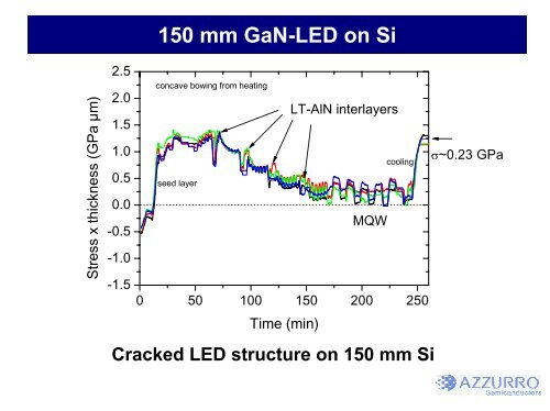
Stress x thickness (GPa µm)<br />
2.5<br />
2.0<br />
1.5<br />
1.0<br />
0.5<br />
0.0<br />
-0.5<br />
-1.0<br />
-1.5<br />
150 mm <strong>GaN</strong>-LED on Si<br />
concave bow<strong>in</strong>g from heat<strong>in</strong>g<br />
seed layer<br />
LT-AlN <strong>in</strong>terlayers<br />
cool<strong>in</strong>g<br />
0 50 100 150 200 250<br />
Time (m<strong>in</strong>)<br />
MQW<br />
Cracked LED structure on 150 mm Si<br />
σ~0.23 GPa