Memory Reliability, Availability, and Serviceability Features - Dell
Memory Reliability, Availability, and Serviceability Features - Dell
Memory Reliability, Availability, and Serviceability Features - Dell

Create successful ePaper yourself
Turn your PDF publications into a flip-book with our unique Google optimized e-Paper software.
SYSTEM ARCHITECTURE<br />
2<br />
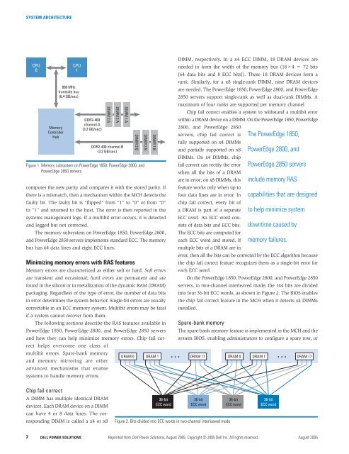
CPU<br />
0<br />
<strong>Memory</strong><br />
Controller<br />
Hub<br />
computes the new parity <strong>and</strong> compares it with the stored parity. If<br />
there is a mismatch, then a mechanism within the MCH detects the<br />
faulty bit. The faulty bit is “flipped” from “1” to “0” or from “0”<br />
to “1” <strong>and</strong> returned to the host. The error is then reported in the<br />
systems management logs. If a multibit error occurs, it is detected<br />
<strong>and</strong> logged but not corrected.<br />
The memory subsystem on PowerEdge 1850, PowerEdge 2800,<br />
<strong>and</strong> PowerEdge 2850 servers implements st<strong>and</strong>ard ECC. The memory<br />
bus has 64 data lines <strong>and</strong> eight ECC lines.<br />
Minimizing memory errors with RAS features<br />
<strong>Memory</strong> errors are characterized as either soft or hard. Soft errors<br />
are transient <strong>and</strong> occasional; hard errors are permanent <strong>and</strong> are<br />
found in the silicon or in metallization of the dynamic RAM (DRAM)<br />
packaging. Regardless of the type of error, the number of data bits<br />
in error determines the system behavior. Single-bit errors are usually<br />
correctable in an ECC memory system. Multibit errors may be fatal<br />
if a system cannot recover from them.<br />
The following sections describe the RAS features available in<br />
PowerEdge 1850, PowerEdge 2800, <strong>and</strong> PowerEdge 2850 servers<br />
<strong>and</strong> how they can help minimize memory errors. Chip fail cor-<br />
rect helps overcome one class of<br />
multibit errors. Spare-bank memory<br />
<strong>and</strong> memory mirroring are other<br />
advanced mechanisms that enable<br />
systems to h<strong>and</strong>le memory errors.<br />
Chip fail correct<br />
CPU<br />
1<br />
800 MHz<br />
frontside bus<br />
(6.4 GB/sec)<br />
DDR2-400<br />
channel A<br />
(3.2 GB/sec)<br />
Figure 1. <strong>Memory</strong> subsystem on PowerEdge 1850, PowerEdge 2800, <strong>and</strong><br />
PowerEdge 2850 servers<br />
A DIMM has multiple identical DRAM<br />
devices. Each DRAM device on a DIMM<br />
can have 4 or 8 data lines. The cor-<br />
responding DIMM is called a x4 or x8<br />
DIMM 3 A<br />
DIMM 2 A<br />
DDR2-400 channel B<br />
(3.2 GB/sec)<br />
DIMM 1 A<br />
DIMM 3 B<br />
DIMM 2 B<br />
DIMM 1 B<br />
DIMM, respectively. In a x4 ECC DIMM, 18 DRAM devices are<br />
needed to form the width of the memory bus (18×4 = 72 bits<br />
[64 data bits <strong>and</strong> 8 ECC bits]). These 18 DRAM devices form a<br />
rank. Similarly, for a x8 single-rank DIMM, nine DRAM devices<br />
are needed. The PowerEdge 1850, PowerEdge 2800, <strong>and</strong> PowerEdge<br />
2850 servers support single-rank as well as dual-rank DIMMs. A<br />
maximum of four ranks are supported per memory channel.<br />
Chip fail correct enables a system to withst<strong>and</strong> a multibit error<br />
within a DRAM device on a DIMM. On the PowerEdge 1850, PowerEdge<br />
2800, <strong>and</strong> PowerEdge 2850<br />
servers, chip fail correct is<br />
fully supported on x4 DIMMs<br />
<strong>and</strong> partially supported on x8<br />
DIMMs. On x4 DIMMs, chip<br />
fail correct can rectify the error<br />
when all the bits of a DRAM<br />
are in error; on x8 DIMMs, this<br />
feature works only when up to<br />
four data lines are in error. In<br />
chip fail correct, every bit of<br />
a DRAM is part of a separate<br />
ECC word. An ECC word con-<br />
sists of data bits <strong>and</strong> ECC bits.<br />
The ECC bits are computed for<br />
each ECC word <strong>and</strong> stored. If<br />
multiple bits of a DRAM are in<br />
error, then all the bits can be corrected by the ECC algorithm because<br />
the chip fail correct feature recognizes them as a single-bit error for<br />
each ECC word.<br />
On the PowerEdge 1850, PowerEdge 2800, <strong>and</strong> PowerEdge 2850<br />
servers, in two-channel interleaved mode, the 144 bits are divided<br />
into four 36-bit ECC words, as shown in Figure 2. The BIOS enables<br />
the chip fail correct feature in the MCH when it detects x4 DIMMs<br />
installed.<br />
Spare-bank memory<br />
The spare-bank memory feature is implemented in the MCH <strong>and</strong> the<br />
system BIOS, enabling administrators to configure a spare row, or<br />
DRAM 0 DRAM 1 DRAM 17 DRAM 0 DRAM 1 DRAM 17<br />
36-bit<br />
ECC word<br />
36-bit<br />
ECC word<br />
Figure 2. Bits divided into ECC words in two-channel interleaved mode<br />
36-bit<br />
ECC word<br />
The PowerEdge 1850,<br />
PowerEdge 2800, <strong>and</strong><br />
PowerEdge 2850 servers<br />
include memory RAS<br />
capabilities that are designed<br />
to help minimize system<br />
downtime caused by<br />
memory failures.<br />
36-bit<br />
ECC word<br />
DELL POWER SOLUTIONS Reprinted from <strong>Dell</strong> Power Solutions, August 2005. Copyright © 2005 <strong>Dell</strong> Inc. All rights reserved. August 2005