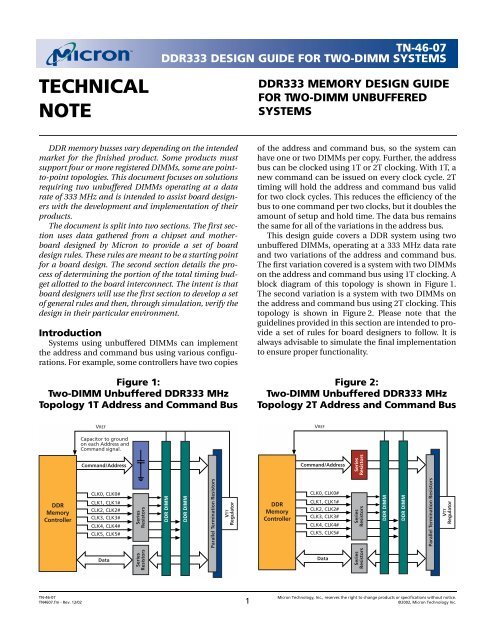
TECHNICAL NOTE - Micron
TECHNICAL NOTE - Micron
TECHNICAL NOTE - Micron

You also want an ePaper? Increase the reach of your titles
YUMPU automatically turns print PDFs into web optimized ePapers that Google loves.
<strong>TECHNICAL</strong><br />
<strong>NOTE</strong><br />
DDR memory busses vary depending on the intended<br />
market for the finished product. Some products must<br />
support four or more registered DIMMs, some are pointto-point<br />
topologies. This document focuses on solutions<br />
requiring two unbuffered DIMMs operating at a data<br />
rate of 333 MHz and is intended to assist board designers<br />
with the development and implementation of their<br />
products.<br />
The document is split into two sections. The first section<br />
uses data gathered from a chipset and motherboard<br />
designed by <strong>Micron</strong> to provide a set of board<br />
design rules. These rules are meant to be a starting point<br />
for a board design. The second section details the process<br />
of determining the portion of the total timing budget<br />
allotted to the board interconnect. The intent is that<br />
board designers will use the first section to develop a set<br />
of general rules and then, through simulation, verify the<br />
design in their particular environment.<br />
Introduction<br />
Systems using unbuffered DIMMs can implement<br />
the address and command bus using various configurations.<br />
For example, some controllers have two copies<br />
Figure 1:<br />
Two-DIMM Unbuffered DDR333 MHz<br />
Topology 1T Address and Command Bus<br />
VREF<br />
Capacitor to ground<br />
on each Address and<br />
Command signal.<br />
Command/Address<br />
CLK0, CLK0#<br />
CLK1, CLK1#<br />
DDR<br />
CLK2, CLK2#<br />
DIMM<br />
Memory<br />
CLK3, CLK3#<br />
Controller DDR<br />
CLK4, CLK4#<br />
CLK5, CLK5#<br />
Data<br />
Series<br />
Resistors<br />
Series<br />
Resistors<br />
TN-46-07<br />
DDR333 DESIGN GUIDE FOR TWO-DIMM SYSTEMS<br />
DDR DIMM<br />
Parallel Termination Resistors<br />
VTT<br />
Regulator<br />
DDR333 MEMORY DESIGN GUIDE<br />
FOR TWO-DIMM UNBUFFERED<br />
SYSTEMS<br />
of the address and command bus, so the system can<br />
have one or two DIMMs per copy. Further, the address<br />
bus can be clocked using 1T or 2T clocking. With 1T, a<br />
new command can be issued on every clock cycle. 2T<br />
timing will hold the address and command bus valid<br />
for two clock cycles. This reduces the efficiency of the<br />
bus to one command per two clocks, but it doubles the<br />
amount of setup and hold time. The data bus remains<br />
the same for all of the variations in the address bus.<br />
This design guide covers a DDR system using two<br />
unbuffered DIMMs, operating at a 333 MHz data rate<br />
and two variations of the address and command bus.<br />
The first variation covered is a system with two DIMMs<br />
on the address and command bus using 1T clocking. A<br />
block diagram of this topology is shown in Figure 1.<br />
The second variation is a system with two DIMMs on<br />
the address and command bus using 2T clocking. This<br />
topology is shown in Figure2. Please note that the<br />
guidelines provided in this section are intended to provide<br />
a set of rules for board designers to follow. It is<br />
always advisable to simulate the final implementation<br />
to ensure proper functionality.<br />
Figure 2:<br />
Two-DIMM Unbuffered DDR333 MHz<br />
Topology 2T Address and Command Bus<br />
CLK0, CLK0#<br />
CLK1, CLK1#<br />
DDR<br />
CLK2, CLK2#<br />
DIMM<br />
Memory<br />
CLK3, CLK3#<br />
Controller DDR<br />
CLK4, CLK4#<br />
CLK5, CLK5#<br />
TN-46-07 <strong>Micron</strong> Technology, Inc., reserves the right to change products or specifications without notice.<br />
TN4607.fm - Rev. 12/02 1 ©2002, <strong>Micron</strong> Technology Inc.<br />
VREF<br />
Command/Address<br />
Data<br />
Series<br />
Resistors<br />
Series<br />
Resistors<br />
Series<br />
Resistors<br />
DDR DIMM<br />
Parallel Termination Resistors<br />
VTT<br />
Regulator
DDR Signal Grouping<br />
The signals that compose a DDR memory bus can<br />
be broken into three unique groupings, each with their<br />
own configuration and routing rules.<br />
Data Group: Data Strobe DQS[8:0], Data Mask<br />
DQM[8:0], Data DQ[63:0], and Check Bits CB[7:0]<br />
Address and Control Group: Bank Address<br />
BA[1:0], Address A[13:0], and Command Inputs<br />
RAS#, CAS#, and WE#. Note that Clock Enable<br />
CKE[3:0], and Chip Select S[3:0]# are also part of<br />
the command signals but they have different<br />
loading and timing.<br />
Clock Group: Differential Clocks CK[5:0] and<br />
CK#[5:0]<br />
Board Stackup<br />
A two-DIMM DDR channel can be routed on a<br />
four-layer board. The layout should be done using<br />
controlled impedance traces of Zo = 60 ohm (±10%)<br />
characteristic impedance. The example stackup is<br />
shown in Figure 3. The trace impedance is based on a<br />
5-mil-wide trace and 1/2 oz. copper.<br />
Figure 3:<br />
Sample Board Stackup<br />
5.5 mil Pregreg<br />
~42 mil Core<br />
5.5 mil Pregreg<br />
Address and Command Signals -<br />
2T Clocking<br />
On a DDR memory bus, the address and command<br />
signals are unidirectional signals driven by the memory<br />
controller. For DDR333, the address and command<br />
TN-46-07<br />
DDR333 DESIGN GUIDE FOR TWO-DIMM SYSTEMS<br />
Component Side - Signal Layer 1<br />
(0.5 oz. cu.)<br />
Ground Plane<br />
(1 oz. cu.)<br />
Power Plane<br />
(1 oz. cu.)<br />
Solder Side - Signal Layer 2<br />
(0.5 oz. cu.)<br />
bus runs at a clock rate of 167 MHz. The address and<br />
command signals are captured at the DRAM using the<br />
memory clocks. For a system with two unbuffered<br />
DIMMs on a single address and command bus, the<br />
loading on these signals will differ greatly depending<br />
on the type and number of DIMMs installed. A two-<br />
DIMM channel loaded with two double-sided DIMMs<br />
has 36 loads on the address and command signals.<br />
Under this heavy loading, the slew rate on the address<br />
bus is slow. The reduced slew rate makes it difficult, if<br />
not impossible, to meet the setup and hold times at the<br />
DRAM. To address this issue, the controller can use 2T<br />
address timing—increasing the time available for the<br />
address command bus by one clock period. Note that<br />
CS and CKE timing are not changed between 1T and<br />
2T addressing.<br />
Routing Rules<br />
It is important that the address and command lines<br />
be referenced to a solid ground or power plane. On a<br />
four-layer board, the address and command would<br />
typically be routed on the second signal layer referenced<br />
to a solid power plane. The system address and<br />
command signals should be ground or power referenced<br />
over the entire bus to provide a low-impedance<br />
current return path. The address and command signals<br />
should be kept from the data group signals, from<br />
the controller to the first DIMM. Address and command<br />
signals are captured at the DIMM using the<br />
clock signals, so they must maintain a length relationship<br />
to the clock signals at the DIMM.<br />
Figure 4:<br />
DDR Address and Command Signal<br />
Group Routing Topology<br />
Pad on Die Pin on Package<br />
DDR<br />
Memory<br />
Controller<br />
Address and<br />
Control<br />
DIMM1 DIMM2<br />
A B<br />
C D E<br />
TN-46-07 <strong>Micron</strong> Technology, Inc., reserves the right to change products or specifications without notice.<br />
TN4607.fm - Rev 12/02 2 ©2002, <strong>Micron</strong> Technology Inc.<br />
Rs<br />
Rp<br />
VTT
Table 1: Address and Command<br />
Group Routing Rules<br />
LENGTH<br />
A = Obtain from DRAM controller vendor.<br />
(A is the length from the die pad to the ball on the<br />
ASIC package.)<br />
B = 1.5in.–2.8in.<br />
C = 0.4in.–0.6in.<br />
D = 0.425in.<br />
E = 0.2in.–0.55in.<br />
Total: A + B + C = 2.4in.–3.2in.<br />
LENGTH MATCHING<br />
±100 mils of memory clock length at the DIMM*<br />
TRACE<br />
Trace Width = 5 mils<br />
Trace Space = 15 mils reducing to 11.5 mils going<br />
between the pins of the DIMM.<br />
Trace Space from DIMM pins = 7 mils<br />
Trace Space to other signal groups = 20 mils<br />
*This value is controller-dependent; see Routing Rules on<br />
page 8.<br />
Series Resistors (Rs)<br />
Location: The series resistors should be located<br />
near the first DIMM for ease of routing.<br />
Value: The value of Rs can vary depending on the<br />
bus topology.<br />
Range: 10 ohms–25 ohms*<br />
Recommended: 20 ohms*<br />
Parallel/Pull-up Resistor (Rp) Termination<br />
Resistor<br />
Location: The parallel termination resistors<br />
should be placed behind the last DIMM slot and<br />
attached to the VTT power island.<br />
Value: The value of the parallel resistor can vary<br />
depending on the bus topology.<br />
Range: 25 ohms–56 ohms*<br />
Recommended: 36 ohms*<br />
*A recommended value. A range of values is provided<br />
for simulation when there is a need to deviate from the<br />
recommendation.<br />
TN-46-07<br />
DDR333 DESIGN GUIDE FOR TWO-DIMM SYSTEMS<br />
Address and Command Signals -<br />
1T Clocking<br />
On a DDR memory bus, the address and command<br />
signals are unidirectional signals always driven by the<br />
memory controller. For DDR333, the address runs at a<br />
clock rate of 167 MHz. The address and command signals<br />
are captured at the DRAM using the memory<br />
clocks. For a system with two unbuffered DIMMs on a<br />
single address and command bus, the loading on these<br />
signals will differ greatly depending on the type and<br />
number of DIMMs installed. A two-DIMM channel<br />
loaded with two double-sided DIMMs has 36 loads on<br />
the address and command signals. The heavy capacitive<br />
load causes a significant reduction in signal slew<br />
rate and voltage margin at the DRAM. The reduced<br />
voltage margin causes a reduction in timing margin. As<br />
a result, setup and hold times at the DRAM may not be<br />
met.<br />
To address the poor margin, <strong>Micron</strong> has developed<br />
a compensated bus topology. This topology uses a<br />
capacitor to ground in place of the series damping<br />
resistor. A block diagram of this topology is shown in<br />
Figure 7.<br />
Figure 5 and Figure 6 are scope captures taken off<br />
two address signals on the same system. The boxes<br />
drawn in the center of the address eye show the setup<br />
and hold times at VIH and VIL DC. Both signals are captured<br />
in a system populated with two double-sided<br />
DIMMs. This is the worst-case address loading situation<br />
in this type of system. All measurements are taken<br />
at room temperature and nominal voltage. The<br />
address signal in Figure 5 is using a series and parallel<br />
resistor topology. As one can see, the address signal<br />
has a slow slew rate and a low maximum VIH. The combined<br />
result is a severe reduction in address setup and<br />
hold times. Under corner conditions, it is possible for<br />
this architecture to violate the DRAM setup and hold<br />
times, resulting in unstable system operation. In<br />
Figure 6, the address line is using the compensated<br />
capacitor architecture. The scope capture clearly<br />
shows the improved signal quality and larger address<br />
valid window.<br />
TN-46-07 <strong>Micron</strong> Technology, Inc., reserves the right to change products or specifications without notice.<br />
TN4607.fm - Rev 12/02 3 ©2002, <strong>Micron</strong> Technology Inc.
Figure 5:<br />
Uncompensated Address Line<br />
Figure 6:<br />
Compensated Address Line<br />
Routing Rules<br />
It is important that the address and command lines<br />
be referenced to a solid ground or power plane. On a<br />
four-layer board, the address and command would<br />
typically be routed on the second signal layer referenced<br />
to a solid power plane. The system address and<br />
command signals should be ground or power referenced<br />
over the entire bus to provide a low-impedance<br />
current return path. The address and command signals<br />
should be kept from the data group signals, from<br />
the controller to the first DIMM. Address and com-<br />
TN-46-07<br />
DDR333 DESIGN GUIDE FOR TWO-DIMM SYSTEMS<br />
Figure 7:<br />
DDR Address and Command Signal<br />
Group Routing Topology<br />
Pad on Die Pin on Package<br />
DDR<br />
Memory<br />
Controller<br />
Address and<br />
Control<br />
DIMM1 DIMM2<br />
A B<br />
C D E<br />
Table 2: Address and Command<br />
Group Routing Rules<br />
LENGTH<br />
A = Obtain from DRAM controller vendor.<br />
(A is the length from the die pad to the ball on the<br />
ASIC package.)<br />
B = 0.4in.–1.4in.<br />
C = 1.6in.–2.2in.<br />
D = 0.425in.<br />
E = 0.2in.–0.55in.<br />
Total: A + B + C = 2.4in.–3.2in.<br />
LENGTH MATCHING<br />
±100 mils of memory clock length at the DIMM*<br />
TRACE<br />
Trace Space = 15 mils reducing to 11.5 mils going<br />
between the pins of the DIMM.<br />
Trace Space from DIMM pins = 7 mils<br />
Trace Space to other signal groups = 20 mils<br />
*This value is controller-dependent; see Routing Rules<br />
on page 8.<br />
mand signals are captured at the DIMM using the<br />
clock signals, so they must maintain a length relationship<br />
to the clock signals at the DIMM.<br />
Compensation Capacitor (CCOMP)<br />
Location: CCOMP should be located such that<br />
lengths B and C are close to equal.<br />
Value: The value of CCOMP can vary depending<br />
on the bus topology.<br />
Range: 45pF–82pF*<br />
Recommended: 82pF*<br />
TN-46-07 <strong>Micron</strong> Technology, Inc., reserves the right to change products or specifications without notice.<br />
TN4607.fm - Rev 12/02 4 ©2002, <strong>Micron</strong> Technology Inc.<br />
CCOMP<br />
Rp<br />
VTT
Parallel/Pull-Up Resistor (Rp)<br />
Termination Resistor<br />
Location: The parallel termination resistors<br />
should be placed behind the last DIMM slot and<br />
attached to the VTT power island.<br />
Value: The value of the parallel resistor can vary<br />
depending on the bus topology.<br />
Range: 25 ohms–56 ohms*<br />
Recommended: 36 ohms*<br />
*A recommended value. A range of values is provided<br />
for simulation when there is a need to deviate from the<br />
recommendation.<br />
Data Signals<br />
In a DDR system, the data is captured by the memory<br />
and the controller using the data strobe rather than<br />
the clock. To achieve the double data rate, data is captured<br />
on the rising and falling edges of the data strobe.<br />
Each eight bits of data has an associated data strobe<br />
(DQS) and a data mask bit (DM). Since the data is captured<br />
off the strobe, the data bits associated with the<br />
strobe must be length matched closely to their strobe<br />
bit. This group of data and data strobe is referred to as<br />
a byte lane. The length matching between byte lanes is<br />
not as tight as it is within the byte lane. Table 3 shows<br />
the data and data strobe byte lane groups. Figure 8<br />
shows the signals in a single-byte lane and the bus<br />
topology for the data signals.<br />
Routing Rules<br />
It is important that the data lines be referenced to a<br />
solid ground plane because they are operating at twice<br />
the frequency of the address and command signals.<br />
These high-speed data signals require a good ground<br />
return path to avoid degradation of signal quality due<br />
to inductance in the signal return path. The system<br />
memory signals should be ground referenced from the<br />
memory controller to the DIMM connectors and from<br />
DIMM connector to DIMM connector to provide a<br />
low-impedance current return path.<br />
This is accomplished by routing the data signals on<br />
the top layer for the entire length of the signal. The<br />
data signals should not have any vias. To help reduce<br />
cross talk noise, the data strobe signals are shielded on<br />
each side by a 5-mil ground trace.<br />
We recommend stitching shield track to ground<br />
every inch to reduce transient currents.<br />
TN-46-07<br />
DDR333 DESIGN GUIDE FOR TWO-DIMM SYSTEMS<br />
Table 3: Data to Data Strobe<br />
Grouping<br />
DATA DATA STROBE DATA MASK<br />
DQ[7:0] DQS 0 DM 0<br />
DQ[15:8] DQS 1 DM 1<br />
DQ[23:16] DQS 2 DM 2<br />
DQ[31:24] DQS 3 DM 3<br />
DQ[39:32] DQS 4 DM 4<br />
DQ[47:40] DQS 5 DM 5<br />
DQ[55:48] DQS 6 DM 6<br />
DQ[63:56] DQS 7 DM 7<br />
CB[7:0] DQS 8 DM 8<br />
Figure 8:<br />
DDR Data Byte Lane Routing Topology<br />
Pad on Die Pin on Package<br />
DIMM1 DIMM2<br />
DQ Byte Group X Rs<br />
A B<br />
DQS[X]<br />
C D E<br />
A B<br />
DM[X]<br />
C D E<br />
A B<br />
C D E<br />
DDR<br />
Memory<br />
Controller<br />
Table 4: Data Group Routing Rules<br />
LENGTH<br />
A = Obtain from DRAM controller vendor. (A is the<br />
length from the die pad to the ball on the ASIC<br />
package.)<br />
B = 1.5in.–2.8in.<br />
C = 0.4in.–0.6in.<br />
D = 0.425in.<br />
E = 0.2in.–0.55in.<br />
Total: A + B + C = 2.4in.–3.2in.<br />
LENGTH MATCHING IN DATA/STROBE BYTE LANE<br />
±100 mils from data strobe<br />
LENGTH MATCHING BYTE LANE TO BYTE LANE<br />
±0.5in. of memory clock length<br />
TRACE<br />
Trace Width = 5 mils<br />
Trace Space = 15 mils reducing to 11.5 mils going<br />
between the pins of the DIMM.<br />
Trace Space from DIMM pins = 7 mils<br />
Trace Space to other signal groups = 20 mils<br />
TN-46-07 <strong>Micron</strong> Technology, Inc., reserves the right to change products or specifications without notice.<br />
TN4607.fm - Rev 12/02 5 ©2002, <strong>Micron</strong> Technology Inc.<br />
Rp<br />
VTT
Clock Signals<br />
The memory clocks CK[5:0] and CK#[5:0] are used<br />
by the DRAM on a DDR bus to capture the address and<br />
command data. Unbuffered DIMMs require three<br />
clock pairs per DIMM. Some DDR memory controllers<br />
will drive all of these clocks, and others will require an<br />
external clock driver to generate these signals. In this<br />
example, it is assumed that the memory controller will<br />
drive the six clock pairs required for a two-DIMM<br />
unbuffered system. Clocks are differential signals, so<br />
they do not get connected to VTT like the other signals<br />
of a DDR bus. The clocks are differential pairs and<br />
must be routed as a differential pair. Each clock pair is<br />
differentially terminated on the DIMM by a 120 ohm<br />
resistor. Figure 9 shows the routing topology used for<br />
the clocks. In this figure, only one of the three clock<br />
pairs required by each DIMM is shown.<br />
Series Resistors (Rs)<br />
Location: The series resistors should be located<br />
near the first DIMM for ease of routing.<br />
Value: The value of the series resistor can vary<br />
depending on the bus topology.<br />
Range: 10 ohms–25 ohms*<br />
Recommended: 20 ohms*<br />
Parallel/Pull-Up Resistor (Rp)<br />
Termination Resistor<br />
Location: The parallel termination resistors<br />
should be placed behind the last DIMM slot and<br />
attached to the VTT power island.<br />
Value: The value of the parallel resistor can vary<br />
depending on the bus lengths used.<br />
Range: 25 ohms–56 ohms*<br />
Recommended: 36 ohms*<br />
*A recommended value. A range of values is provided<br />
for simulation when there is a need to deviate from the<br />
recommendation.<br />
TN-46-07<br />
DDR333 DESIGN GUIDE FOR TWO-DIMM SYSTEMS<br />
Figure 9:<br />
DDR Clock Signal Group Routing<br />
Topology<br />
Pad on Die Pin on Package<br />
CK[2:0] Rs<br />
A B<br />
CK#[2:0]<br />
C<br />
A B<br />
C<br />
A<br />
CK[5:3]<br />
B<br />
CK#[5:3]<br />
C2<br />
A<br />
DDR<br />
Memory<br />
Controller<br />
B<br />
C2<br />
DIMM1 DIMM2<br />
Routing Rules<br />
The clocks are routed as a differential pair from the<br />
controller to the DIMM. The clocks are used to capture<br />
the address signals at the DIMM, so they must maintain<br />
a length relationship to the address signals at the<br />
DIMM they are connected to. Different controllers<br />
handle the address clock relationship differently—<br />
some controllers have the ability to adjust the address<br />
to clock delay and others use a fixed delay. Memory<br />
controllers with a variable delay can better center the<br />
clock in the address valid eye over varying load conditions.<br />
Controllers with a fixed delay may require different<br />
routing of the clocks to compensate for different<br />
loading on the clock versus the address. The rules in<br />
this section are based on a controller that has variable<br />
clock delay.<br />
DDR Memory Power Supply<br />
Requirements<br />
A DDR bus implementation requires three separate<br />
power supplies. The DRAM and the memory portion of<br />
the controller require a 2.5-volt supply. The 2.5-volt<br />
supply provides power for the DRAM core and I/O as<br />
well as at least the I/O of the DRAM controller. The<br />
second power supply is VREF, which is used as a reference<br />
voltage by the DRAM and the controller. The<br />
third supply is VTT, which is the termination supply of<br />
the bus. Table 6 lists the tolerances of each of these<br />
supplies.<br />
TN-46-07 <strong>Micron</strong> Technology, Inc., reserves the right to change products or specifications without notice.<br />
TN4607.fm - Rev 12/02 6 ©2002, <strong>Micron</strong> Technology Inc.
Table 5: Clock Group Routing Rules<br />
LENGTH<br />
A = Obtain from DRAM controller vendor.<br />
(A is the length from the die pad to the ball on the<br />
ASIC package.)<br />
B = 1.5in.–2.8in.<br />
C = 0.4in.–0.6in.<br />
C2 =0.825in.–1.025in.<br />
LENGTH MATCHING<br />
±30 mils for CKE to CKE#<br />
±30 mils clock pair to clock pair at the DIMM<br />
TRACE<br />
Trace Width = 10 mils<br />
Trace Space = 5 mils<br />
Trace Space to other signal groups = 20 mils<br />
Series Resistor (Rs)<br />
Location: The series resistor is located near the<br />
driver.<br />
Value: The value of the series resistor can vary<br />
depending on the bus topology.<br />
Range: 22 ohms–25 ohms<br />
Recommended: 22 ohms<br />
MVTT Voltage<br />
The memory termination voltage, MVTT, requires<br />
current at a voltage level of 1.25 VDC. See Figure 6 for<br />
the VTT tolerance. VTT must be generated by a regulator<br />
that is able to sink and source current while still<br />
maintaining the tight voltage regulation.<br />
VREF and VTT must track variations in VDD over<br />
voltage, temperature, and noise ranges.<br />
VTT of the transmitting device must track VREF of<br />
the receiving device.<br />
Table 6: Required Voltages<br />
TN-46-07<br />
DDR333 DESIGN GUIDE FOR TWO-DIMM SYSTEMS<br />
MVTT Layout Recommendations<br />
Place the MVTT island on the component-side<br />
signals layer at the end of the bus behind the last<br />
DIMM slot.<br />
Use a wide-island trace for current capacity.<br />
Place VTT generator as close to termination<br />
resistors as possible to minimize impedance<br />
(inductance).<br />
Place one or two 0.1µf decoupling caps by each<br />
termination RPACK on the MVTT island to minimize<br />
the noise on VTT. Other bulk (10µf–22µf)<br />
decoupling is also recommended to be placed on<br />
the MVTT island.<br />
MVREF Voltage<br />
The memory reference voltage, MVREF, requires<br />
approximately 3mA of current at a voltage level of 1/2<br />
VDD with a tolerance shown in Table 6. VREF can be<br />
generated using a simple resistor divider with one percent<br />
or better accuracy. VREF must track 1/2 of VDD<br />
over voltage, noise, and temperature changes.<br />
Peak-to-peak AC noise on VREF may not exceed<br />
±2 percent VREF (DC).<br />
MVREF Layout Recommendations<br />
Use 30-mil trace between decoupling cap and<br />
destination.<br />
Maintain a 25-mil clearance from other nets.<br />
Simplify implementation by routing VREF on the<br />
top signal trace layer.<br />
Isolate VREF and/or shield with ground.<br />
Decouple using distributed 0.01µf and 0.1µf<br />
capacitors by the regulator, controller, and DIMM<br />
slots. Place one 0.01µf and 0.1µf near pin one of<br />
each DIMM. Place one 0.1µf near the source of<br />
VREF, one near the VREF pin on the controller, and<br />
two between the controller and the first DIMM.<br />
SYMBOL PARAMETER MIN TYPICAL MAX UNIT<br />
VDD (V25) Device Supply Voltage 2.3 2.5 2.7 V<br />
VREF Memory Reference Voltage (0.5 × VDD) - 25mV 0.5 × VDD (0.5 × VDD) + 25mV V<br />
VTT Memory Termination Voltage VREF - 640mV VREF VREF + 40mV V<br />
TN-46-07 <strong>Micron</strong> Technology, Inc., reserves the right to change products or specifications without notice.<br />
TN4607.fm - Rev 12/02 7 ©2002, <strong>Micron</strong> Technology Inc.
Timing Budget<br />
The previous section is useful for getting an idea of<br />
how the DDR memory bus functions and the general<br />
relationship between the signals on the bus. However,<br />
if a design should deviate from the given example, the<br />
routing rules for the design can change. Since it is<br />
unlikely that every design will follow the given example<br />
exactly, it is important to simulate the design. One<br />
of the objectives of simulation is to determine if the<br />
design will meet the signal timing requirements of the<br />
DRAM and DDR controller. To meet this objective, a<br />
timing budget must be generated. This section shows<br />
how to use the data provided in the DDR DRAM and<br />
DDR controller data sheets to determine the amount<br />
of the total timing budget that the board interconnect<br />
can consume.<br />
Table 7: DDR Write Budget<br />
<strong>NOTE</strong>:<br />
These are worst-case slow numbers (100C, 2.375V, slow process).<br />
TN-46-07<br />
DDR333 DESIGN GUIDE FOR TWO-DIMM SYSTEMS<br />
DDR Data Write Budget<br />
Table 7 gives a breakdown of the timing budget for<br />
DDR WRITEs at 333 MHz. The portion of the budget<br />
consumed by the DRAM device and by the DDR controller<br />
is fixed and cannot be influenced by the board<br />
designer. The amount of the total budget remaining<br />
after subtracting the portion consumed by the DRAM<br />
and the controller is what remains for the board interconnect.<br />
This is the portion that is used to determine<br />
the bus routing rules. The different components of the<br />
board interconnect are outlined. The board designer<br />
can make trade-offs with trace spacing, length matching,<br />
resistor tolerance, etc., to determine the best interconnect<br />
solution.<br />
ELEMENT SKEW COMPONENT SETUP HOLD UNITS COMMENTS<br />
Transmitter Total Skew at Transmitter 550 550 ps From data sheet<br />
DRAM device<br />
t t DH/ DS 450 450 ps<br />
(from spec) Total Device 450 450 ps From data sheet<br />
Interconnect XTK (cross talk) - DQ 100 100 ps 4 aggressors (a pair on each<br />
side of the victim)<br />
XTK (cross talk) - DQS 30 30 ps 1 shielded victim, 2 aggressors<br />
(PRBS)<br />
ISI - DQ 15 15 ps<br />
ISI - DQS 5 5 ps<br />
Path Matching 15 15 ps Within byte lane:<br />
165 ps/in. × 0.1in.;<br />
motherboard routes account<br />
for memory controller package<br />
skew<br />
Input Capacitance Matching 95 95 ps 4.0pF and 5.0pF loads, strobe<br />
and data shift differently<br />
RTERM VOH/VOL Skew (1%) 20 20 ps<br />
Input Eye Reduction (VREF) 100 100 ps ±75mV included in DRAM<br />
skew; additional =<br />
(±25mV)/(.5 V/ns); this includes<br />
DQ and DQS<br />
Strobe-to-Data Skew 10 +10 ps Strobe shifts relative to data<br />
(1010 pattern vs. PRBS)<br />
Total Interconnect Interconnect Skew 390 390 ps From simulation<br />
Total Budget 3000/2 @ 333 MHz 1500 1500 ps<br />
Total Budget<br />
Consumed by<br />
Controller and DRAM<br />
Transmitter + DRAM 1000 1000 ps<br />
Interconnect Budget Total - (transmitter + DRAM) 500 500 ps Must be greater than amount<br />
consumed by board<br />
interconnect<br />
TN-46-07 <strong>Micron</strong> Technology, Inc., reserves the right to change products or specifications without notice.<br />
TN4607.fm - Rev 12/02 8 ©2002, <strong>Micron</strong> Technology Inc.
Determining DRAM Write Budget<br />
Consumption<br />
The amount of the write budget consumed by the<br />
DRAM is easily obtained from the data sheets. The<br />
DRAM data sheet provides the data input hold time<br />
relative to strobe ( t DH) and the data input setup time<br />
relative to strobe ( t DS). These numbers are entered<br />
directly into the timing budgets for setup and hold.<br />
They account for all of the write timing budget consumed<br />
by the DRAM.<br />
CK<br />
ADDR/<br />
CK<br />
DQS<br />
DQ<br />
TN-46-07<br />
DDR333 DESIGN GUIDE FOR TWO-DIMM SYSTEMS<br />
Figure 10:<br />
Memory Write and ADDR/CMD Timing<br />
Determining DDR Controller Write Budget<br />
Consumption<br />
To calculate the amount of the setup timing budget<br />
consumed by the DDR controller on a DRAM WRITE,<br />
find the value for t DQSU minimum. This is the minimum<br />
amount of time all data will be valid before the<br />
data strobe transitions shown in Figure 10. t DQSU<br />
should take clock asymmetry into account. In an ideal<br />
situation, t DQSU would be equal to 1/4 × t CK. The difference<br />
between 1/4 × t CK and t DQSU is the amount of<br />
the write timing budget consumed by the controller<br />
for setup. From this, the following equation is derived.<br />
Controller setup data valid reduction = 1/4 × t CK -<br />
t DQSU.<br />
To calculate the hold time, use the same equation,<br />
but use t DQHD in place of t DQSU.<br />
T0 T1 T2 T3 T4 T5 T6<br />
t ADSU<br />
t ADHD<br />
t DQSS<br />
t DSH<br />
tDQSU tDQHD TN-46-07 <strong>Micron</strong> Technology, Inc., reserves the right to change products or specifications without notice.<br />
TN4607.fm - Rev 12/02 9 ©2002, <strong>Micron</strong> Technology Inc.<br />
t DSS<br />
A A A A<br />
t WPST
DDR Data Read Budget<br />
Table 8 gives a breakdown of the timing budget for<br />
DDR reads at 333 MHz. The portion of the budget consumed<br />
by the DRAM device and by the DDR controller<br />
is fixed and cannot be influenced by the board<br />
Table 8: DDR Read Budget<br />
<strong>NOTE</strong>:<br />
These are worst-case slow numbers (100C, 2.375V, slow process).<br />
TN-46-07<br />
DDR333 DESIGN GUIDE FOR TWO-DIMM SYSTEMS<br />
designer. The amount of the total budget remaining<br />
after subtracting the portion consumed by the DRAM<br />
and the controller is what remains for the board<br />
interconnect.<br />
ELEMENT SKEW COMPONENT SETUP HOLD UNITS COMMENTS<br />
DRAM device Clock 6 6 ns<br />
(from spec) t t t HP ( CL/ CH[MIN] at 45/55) 2.70 2.70 ns<br />
t DQSQ 350 350 ps<br />
t QHS 500 500 ps<br />
t QH ( t HP - t QHS) 2.20 2.20 ns<br />
t DV ( t HP - t DQSQ - t QHS, or<br />
t QH - t DQSQ)<br />
1.85 1.85 ns<br />
( t CK/2 - t DV)/2 575 575 ps<br />
DRAM Total Total DRAM Data Valid<br />
Reduction<br />
575 575 ps From data sheet<br />
Receiver<br />
(controller)<br />
Total Skew at Receiver 550 550 ps From data sheet<br />
Interconnect XTK (cross talk) - DQ 70 70 ps 4 aggressors (a pair on each<br />
side of the victim)<br />
XTK (cross talk) - DQS 35 35 ps 1 shielded victim, 2 aggressors<br />
(PRBS)<br />
ISI - DQ 50 50 ps Spice-generated eye diagram<br />
ISI - DQS 15 15 ps<br />
Path Matching 20 20 ps Within byte lane:<br />
165 ps/in. × 0.1in.; MB routes<br />
acct. for MC pkg. skew<br />
Rterm VOH/VOL Skew (1%) 20 20 ps<br />
Input Eye Reduction (VREF) 100 100 ps ±75mV included in DRAM<br />
skew; additional =<br />
(±25 mV)/(.5 V/ns); this includes<br />
DQ and DQS<br />
Total Interconnect Total Skew at Interconnect 310 310 ps From simulation<br />
Total Budget 3000/2 @ 333 MHz 1500 1500 ps<br />
Total Budget<br />
Consumed by<br />
Controller and DRAM<br />
Receiver + DRAM 1125 1125 ps<br />
Interconnect Budget Total - (transmitter + DRAM) 375 375 ps Must be greater than amount<br />
consumed by board<br />
interconnect<br />
TN-46-07 <strong>Micron</strong> Technology, Inc., reserves the right to change products or specifications without notice.<br />
TN4607.fm - Rev 12/02 10 ©2002, <strong>Micron</strong> Technology Inc.
DQS<br />
DQ (last data valid)<br />
DQ (first data no longer valid)<br />
All DQs and DQS, collectively<br />
CK<br />
DQS<br />
DQ (last data valid)<br />
DQ (first data no<br />
longer valid)<br />
DQ (byte), collectively<br />
Determining DRAM Read Budget<br />
Consumption<br />
Figure 11 shows how the information from the<br />
DRAM data sheet affects the total data valid window as<br />
the data is driven from the DRAM device. This information<br />
is used in the timing budget to determine the<br />
amount of the total data timing budget that is consumed<br />
by the DRAM device. The total budget for the<br />
data is half the clock period. This time is halved again<br />
to determine the time allowed for setup and hold.<br />
TN-46-07<br />
DDR333 DESIGN GUIDE FOR TWO-DIMM SYSTEMS<br />
Figure 11:<br />
DRAM Read Data Valid<br />
t DQSQ = 350ps<br />
t QH = 2.2ns<br />
DVW = 1.85ns<br />
Figure 12:<br />
Read Data Timing<br />
t CK/2 = 3.0ns<br />
t HP = 2.7ns ( t CK@45/55) Clock Duty Cyle = 45/55%<br />
Data Valid Window<br />
t QHS = 500ps<br />
T0 T1 T2 T3 T4<br />
tHP tHP tHP tHP tHP tHP tHP t DQSQ<br />
t QH<br />
t DV<br />
t DQSQ t DQSQ t DQSQ<br />
D D D D<br />
D D D D<br />
D D D D<br />
D D D D<br />
D D D D<br />
D D D D<br />
D D D D<br />
D D D D<br />
t QH t QH t QH<br />
t DV<br />
Using the DRAM data sheet and filling in numbers for<br />
the timing parameters in Figure 11, the total data valid<br />
window at the DRAM can be calculated using the following<br />
equation:<br />
DVW = t HP - t DQSQ - t QHS<br />
t<br />
CK/2 - DVW/2 = DRAM data valid reduction.<br />
The DRAM data valid reduction is used in the timing<br />
budget for setup and hold.<br />
TN-46-07 <strong>Micron</strong> Technology, Inc., reserves the right to change products or specifications without notice.<br />
TN4607.fm - Rev 12/02 11 ©2002, <strong>Micron</strong> Technology Inc.<br />
t DV<br />
t DV
Determining DDR Controller Read<br />
Budget Consumption<br />
When read data is received at the controller from<br />
the DRAM, the strobe is edge aligned with the data. It<br />
is the responsibility of the controller to delay the<br />
strobe and then use the delayed strobe to capture the<br />
read data. The controller will have some minimum<br />
value it can accept for a data valid window. Internally,<br />
the controller has a minimum setup and hold time that<br />
the data must maintain from the internally delayed<br />
strobe. Half the data valid window is the setup or hold<br />
time required by the controller plus any controllerintroduced<br />
signal skew and strobe centering uncertainty.<br />
The timing diagram example in Figure 12 shows<br />
the timing parameters required for calculating the data<br />
valid window. t DQSQ is the maximum delay from the<br />
last data signal to go valid after the strobe transitions.<br />
t QH is the minimum time all data must remain valid<br />
after strobe transitions. Use the following equation to<br />
obtain t DV:<br />
t t t DV = QH - DQSQ.<br />
Assuming tDV is split evenly between setup and<br />
hold, the portion of the timing budget consumed by<br />
the controller for setup and hold is 1/2 tDV. For the<br />
controller used in this example, an even split between<br />
setup and hold can be assumed because the controller<br />
determining the center of the data eye during the<br />
bootup routine and the DLL maintains this relationship<br />
over temperature and voltage variations.<br />
Address Timing Budget<br />
Table 9 gives a breakdown of the timing budget for<br />
1T address and command at a 167 MHz clock rate. The<br />
portion of the budget consumed by the DRAM device<br />
and the DDR controller is fixed and cannot be influenced<br />
by the board designer. The amount of the total<br />
budget remaining after subtracting the portion consumed<br />
by the DRAM and the controller is what<br />
remains for the board interconnect.<br />
TN-46-07<br />
DDR333 DESIGN GUIDE FOR TWO-DIMM SYSTEMS<br />
Determining DRAM Address Budget<br />
Consumption<br />
The portion of the address budget consumed by the<br />
DRAM is obtained by getting the value of t IS for setup<br />
and t IH for hold. t IH and t IS are the setup and hold<br />
times required by the DRAM inputs. For systems with<br />
heavy loading on the address and command lines, the<br />
value in the data sheet must be derated depending on<br />
the slew rate. For <strong>Micron</strong> DDR DRAM, the setup time is<br />
raised by 50ps for each 100 mV/ns that the slew rate<br />
drops below 0.5 V/ns. The hold time is not changed.<br />
Determining Controller Address Budget<br />
Consumption<br />
The DRAM controller will provide a minimum setup<br />
and hold time for the address and command signals<br />
with respect to clock. This is the amount of the setup<br />
and hold budget consumed by the controller.<br />
Clock to Data Strobe Relationship<br />
The DDR DRAM and the DDR controller must move<br />
the data from the data strobe clocking domain into the<br />
DDR clock domain when the data is latched internally.<br />
Due to this requirement, the data strobe must maintain<br />
a relationship to the DDR clock. For the DDR<br />
DRAM, this relationship is specified by t DQSS. This<br />
timing parameter states that after a WRITE command,<br />
the data strobe must transition 0.75 to 1.25 × t CK.<br />
Figure 10 shows the DDR controller also specifies a<br />
t DQSS timing parameter. This is the time after the<br />
WRITE command that the data strobe will transition.<br />
For the controller in this example, t DQSS = ±0.06 × t CK.<br />
The following equation is used to calculate the amount<br />
of clock to data strobe skew that is left for consumption<br />
by the board interconnect:<br />
Interconnect budget = DRAM t DQSS - Controller<br />
t DQSS<br />
Using this equation, it is apparent that this is not<br />
one of the strict timing requirements of a DDR channel.<br />
If the clocks are routed so they are between the<br />
shortest and longest strobe lengths, the designer gains<br />
some leeway in the data strobe to data strobe byte lane<br />
routing restrictions.<br />
TN-46-07 <strong>Micron</strong> Technology, Inc., reserves the right to change products or specifications without notice.<br />
TN4607.fm - Rev 12/02 12 ©2002, <strong>Micron</strong> Technology Inc.
Table 9: Address Timing Budget<br />
<strong>NOTE</strong>:<br />
These are worst-case slow numbers (100C, 2.375V, slow process).<br />
Appendix: Simulation Result Data<br />
TN-46-07<br />
DDR333 DESIGN GUIDE FOR TWO-DIMM SYSTEMS<br />
ELEMENT SKEW COMPONENT SETUP HOLD UNITS COMMENTS<br />
Transmitter Memory Controller<br />
Transmitter<br />
550 550 ps Chipset<br />
Receiver DRAM Skew 850 750 ps t t<br />
IS, IH from DRAM spec (slow<br />
edge). t IS: additional 50ps for<br />
every 0.1 V/ns below 0.5 V/ns<br />
(0.3 V/ns)<br />
Interconnect Cross Talk: Address 640 640 ps 1 victim (1010...), 4 aggressors<br />
(PRBS)<br />
ISI: Address 690 690 ps (PRBS)<br />
Cross Talk: Clock 25 25 ps Spec.<br />
VREF: Reduction 50 50 ps ±75mV included in DRAM<br />
skew; additional =<br />
(±25mV)/(.5 V/ns)<br />
Path Matching 15 15 ps Within byte lane: 165 ps/in. ×<br />
0.1in.; MB routes acct. for MC<br />
pkg. skew<br />
Input Capacitance Matching 105 105 ps 1.5pF for 5 device, 2.5pF for 18<br />
device (1610-1400) = 210 total<br />
Compensating Capacitor 60 60 ps Compensating capacitor<br />
Skew (5%)<br />
5% tolerance<br />
Rterm VOH/VOL Skew (1%) 10 10 ps Estimator tool<br />
Total Interconnect Total Skew at Interconnect 1595 1595 ps<br />
Total Budget 6000 @ 333 MHz 3000 3000 ps 333 MHz bit width<br />
Total Budget<br />
Consumed by<br />
Controller and DRAM<br />
Transmitter + DRAM 1400 1300 ps<br />
Interconnect Budget Total - (Transmitter + DRAM) 1600 1700 ps<br />
Data Bus Simulation Conditions<br />
STANDARD TERMINATION<br />
Rs = 20<br />
Controller Ron = 15<br />
DRAM Ron = 15<br />
Rp = 36 ohms<br />
B = 2,200 mils<br />
C = 400 mils<br />
D = 425 mils<br />
E = 400 mils<br />
Rise Time = 750ps<br />
Data Rate = 333 MHz<br />
TN-46-07 <strong>Micron</strong> Technology, Inc., reserves the right to change products or specifications without notice.<br />
TN4607.fm - Rev 12/02 13 ©2002, <strong>Micron</strong> Technology Inc.
Slot 1<br />
Slot 2<br />
Slot 1<br />
Slot 2<br />
TN-46-07<br />
TN4607.fm - Rev. 12/02<br />
ISI 1 = 9 DD<br />
Apert2 1 = 2.496 SlewR 1 = 1.42<br />
ISI 2 = 11 DD<br />
Apert2 2 = 2.434 SlewR 2 = 1.27<br />
ISI 7 = 29 SS<br />
Apert2 7 = 2.477 SlewR 7 = 1.37<br />
ISI 8 = 26 SS<br />
Apert2 8 = 2.446 SlewR 8 = 1.31<br />
TN-46-07<br />
DDR333 DESIGN GUIDE FOR TWO-DIMM SYSTEMS<br />
Figure 13:<br />
SSTL READs Rs = 20 Rstub = 22 Rp = 36 Pitch = 0.425”<br />
ISI 3 = 23 DS<br />
Apert2 3 = 2.493 SlewR 3 = 1.43<br />
ISI 4 = 11 DS<br />
Apert2 4 = 2.404 SlewR 4 = 1.19<br />
ISI 9 = 25 D–<br />
Apert2 9 = 2.551 SlewR 9 = 1.64<br />
ISI 10 = 30 –D<br />
Apert2 10 = 2.556 SlewR 10 = 1.69<br />
14<br />
ISI 5 = 13 SD<br />
Apert2 5 = 2.471 SlewR 5 = 1.33<br />
ISI 6 = 24 SD<br />
Apert2 6 = 2.464 SlewR6 1 = 1.37<br />
ISI 11 = 28 S–<br />
Apert2 11 = 2.559 SlewR 11 = 1.67<br />
ISI 12 = 31 –S<br />
Apert2 12 = 2.556 SlewR 12 = 1.75<br />
<strong>Micron</strong> Technology, Inc., reserves the right to change products or specifications without notice.<br />
©2002, <strong>Micron</strong> Technology Inc.
Slot 1<br />
Slot 2<br />
Slot 1<br />
Slot 2<br />
TN-46-07<br />
TN4607.fm - Rev. 12/02<br />
ISI 1 = 37 DD<br />
Apert2 1 = 2.033 SlewR 1 = 0.79<br />
ISI 2 = 38 DD<br />
Apert2 2 = 2.076 SlewR 2 = 0.80<br />
ISI 7 = 4 SS<br />
Apert2 7 = 2.516 SlewR 7 = 1.46<br />
ISI 8 = 5 SS<br />
Apert2 8 = 2.470 SlewR 8 = 1.34<br />
TN-46-07<br />
DDR333 DESIGN GUIDE FOR TWO-DIMM SYSTEMS<br />
Figure 14:<br />
SSTL Writes Rs = 20 Rstub = 22 Rp = 36 Pitch = 0.425”<br />
ISI 3 = 21 DS<br />
Apert2 3 = 2.210 SlewR 3 = 0.93<br />
ISI 4 = 20 DS<br />
Apert2 4 = 2.358 SlewR 4 = 1.17<br />
ISI 9 = 3 D–<br />
Apert2 9 = 2.431 SlewR 9 = 1.26<br />
ISI 10 = 8 –D<br />
Apert2 10 = 2.428 SlewR 10 = 1.26<br />
15<br />
ISI 5 = 23 SD<br />
Apert2 5 = 2.476 SlewR 5 = 1.40<br />
ISI 6 = 26 SD<br />
Apert2 6 = 2.243 SlewR6 1 = 0.97<br />
ISI 11 = 3 S–<br />
Apert2 11 = 2.589 SlewR 11 = 1.71<br />
ISI 12 = 3 –S<br />
Apert2 12 = 2.590 SlewR 12 = 1.72<br />
<strong>Micron</strong> Technology, Inc., reserves the right to change products or specifications without notice.<br />
©2002, <strong>Micron</strong> Technology Inc.
Address Bus Simulation Conditions<br />
STANDARD TERMINATION<br />
Rs = 10<br />
Controller Ron = 15<br />
Rp = 33 ohms<br />
B = 2,750 mils<br />
C = 250 mils<br />
D = 425 mils<br />
E = 400 mils<br />
Rise Time = 700ps<br />
2T Cycle @ 83 MHz<br />
A1 address line is simulated.<br />
Waveforms shown are @ U1 memory device for<br />
both the slots<br />
TN-46-07<br />
DDR333 DESIGN GUIDE FOR TWO-DIMM SYSTEMS<br />
COMPENSATED<br />
Fcap = 82pF<br />
Controller Ron = 15<br />
(Except last slide, where it is 25)<br />
Rp = 33 ohms<br />
B = 1,500 mils<br />
C = 1,500 mils<br />
D = 425 mils<br />
E = 400 mils<br />
Rise Time = 700ps<br />
1T Cycle @ 166 MHz<br />
A1 address line is simulated.<br />
Waveforms shown are @ U1 memory device for<br />
both the slots<br />
TN-46-07 <strong>Micron</strong> Technology, Inc., reserves the right to change products or specifications without notice.<br />
TN4607p16.fm - Rev 12/02 16 ©2002, <strong>Micron</strong> Technology Inc.
5,0 ISI 1 = 29<br />
Apert2 1 = 11.036<br />
SlewR 1 = 0.72<br />
5,5 ISI 1 = 22<br />
Apert2 1 = 10.670<br />
SlewR 1 = 0.52<br />
5,9 ISI 1 = 47<br />
Apert2 1 = 10.403<br />
SlewR 1 = 0.43<br />
5,18 ISI 1 = 38<br />
Apert2 1 = 10.115<br />
SlewR 1 = 0.36<br />
TN-46-07<br />
TN4607.fm - Rev. 12/02<br />
TN-46-07<br />
DDR333 DESIGN GUIDE FOR TWO-DIMM SYSTEMS<br />
Figure 15:<br />
Standard Termination, 2T Cycle Slot 1<br />
9,0 ISI 1 = 31<br />
Apert2 1 = 10.634<br />
SlewR 1 = 0.49<br />
9,5 ISI 1 = 13<br />
Apert2 1 = 10.389<br />
SlewR 1 = 0.42<br />
9,9 ISI 1 = 25<br />
Apert2 1 = 10.165<br />
SlewR 1 = 0.38<br />
9,18 ISI 1 = 85<br />
Apert2 1 = 9.831<br />
SlewR 1 = 0.32<br />
17<br />
18,0 ISI 1 = 79<br />
Apert2 1 = 10.279<br />
SlewR 1 = 0.41<br />
18,5 ISI 1 = 15<br />
Apert2 1 = 9.961<br />
SlewR 1 = 0.34<br />
18,9 ISI 1 = 6<br />
Apert2 1 = 9.743<br />
SlewR 1 = 0.31<br />
18,18 ISI 1 = 77<br />
Apert2 1 = 9.392<br />
SlewR 1 = 0.27<br />
<strong>Micron</strong> Technology, Inc., reserves the right to change products or specifications without notice.<br />
©2002, <strong>Micron</strong> Technology Inc.
0,5 ISI 1 = 22<br />
Apert2 1 = 10.982<br />
SlewR 1 = 0.68<br />
5,5 ISI 1 = 14<br />
Apert2 5 = 10.578<br />
SlewR 5 = 0.48<br />
5,9 ISI 5 = 9<br />
Apert25 1 = 10.255<br />
SlewR5 1 = 0.39<br />
5,18 ISI 5 = 17<br />
Apert2 5 = 9.866<br />
SlewR 5 = 0.32<br />
TN-46-07<br />
TN4607.fm - Rev. 12/02<br />
0,9 ISI 1 = 40<br />
Apert2 1 = 10.608<br />
SlewR 1 = 0.49<br />
9,5 ISI 10 = 62<br />
Apert2 10 = 10.249<br />
SlewR 10 = 0.39<br />
9,9 ISI 10 = 41<br />
Apert2 10 = 10.025<br />
SlewR 10 = 0.35<br />
9,18 ISI 10 = 39<br />
Apert2 10 = 9.596<br />
SlewR 10 = 0.29<br />
TN-46-07<br />
DDR333 DESIGN GUIDE FOR TWO-DIMM SYSTEMS<br />
Figure 16:<br />
Standard Termination, 2T Cycle Slot 2<br />
18<br />
0,18 ISI 1 = 77<br />
Apert2 1 = 10.244<br />
SlewR 1 = 0.40<br />
18,5 ISI 2 = 74<br />
Apert2 2 = 9.974<br />
Slew2 = 0.33<br />
18,9 ISI 2 = 6<br />
Apert2 2 = 9.734<br />
SlewR 2 = 0.31<br />
18,18 ISI 2 = 22<br />
Apert2 2 = 9.326<br />
SlewR 2 = 0.26<br />
<strong>Micron</strong> Technology, Inc., reserves the right to change products or specifications without notice.<br />
©2002, <strong>Micron</strong> Technology Inc.
5,0 ISI 1 = 311<br />
Apert2 1 = 4.925<br />
SlewR 1 = 0.77<br />
5,5 ISI 1 = 124<br />
Apert2 1 = 4.955<br />
SlewR 1 = 0.70<br />
5,9 ISI 1 = 226<br />
Apert2 1 = 4.643<br />
SlewR 1 = 0.58<br />
5,18 ISI 1 = 418<br />
Apert2 1 = 4.221<br />
SlewR 1 = 0.43<br />
TN-46-07<br />
TN4607.fm - Rev. 12/02<br />
TN-46-07<br />
DDR333 DESIGN GUIDE FOR TWO-DIMM SYSTEMS<br />
Figure 17:<br />
Compensated, 1T Cycle Slot 1<br />
9,0 ISI 1 = 145<br />
Apert2 1 = 4.998<br />
SlewR 1 = 0.71<br />
9,5 ISI 1 = 19<br />
Apert2 1 = 4.921<br />
SlewR 1 = 0.64<br />
9,9 ISI 1 = 126<br />
Apert2 1 = 4.742<br />
SlewR 1 = 0.60<br />
9,18 ISI 1 = 283<br />
Apert2 1 = 4.476<br />
SlewR 1 = 0.46<br />
19<br />
18,0 ISI 1 = 117<br />
Apert2 1 = 4.848<br />
SlewR 1 = 0.62<br />
18,5 ISI 1 = 160<br />
Apert2 1 = 4.653<br />
SlewR 1 = 0.55<br />
18,9 ISI 1 = 133<br />
Apert2 1 = 4.576<br />
SlewR 1 = 0.53<br />
18,18 ISI 1 = 65<br />
Apert2 1 = 4.422<br />
SlewR 1 = 0.44<br />
<strong>Micron</strong> Technology, Inc., reserves the right to change products or specifications without notice.<br />
©2002, <strong>Micron</strong> Technology Inc.
0,5 ISI 1 = 326<br />
Apert2 1 = 4.907<br />
SlewR 1 = 0.76<br />
5,5 ISI 5 = 45<br />
Apert2 5 = 4.971<br />
SlewR 5 = 0.67<br />
5,9 ISI 5 = 127<br />
Apert25 1 = 4.747<br />
SlewR5 1 = 0.59<br />
5,18 ISI 5 = 291<br />
Apert2 5 = 4.503<br />
SlewR 5 = 0.51<br />
TN-46-07<br />
TN4607.fm - Rev. 12/02<br />
TN-46-07<br />
DDR333 DESIGN GUIDE FOR TWO-DIMM SYSTEMS<br />
Figure 18:<br />
Compensated, 1T Cycle Slot 2<br />
0,9 ISI 1 = 148<br />
Apert2 1 = 4.955<br />
SlewR 1 = 0.69<br />
9,5 ISI 10 = 199<br />
Apert2 10 = 4.723<br />
SlewR 10 = 0.61<br />
9,9 ISI 10 = 186<br />
Apert2 10 = 4.666<br />
SlewR 10 = 0.56<br />
9,18 ISI 10 = 369<br />
Apert2 10 = 4.320<br />
SlewR 10 = 0.47<br />
20<br />
0,18 ISI 1 = 133<br />
Apert2 1 = 4.809<br />
SlewR 1 = 0.60<br />
18,5 ISI 2 = 333<br />
Apert2 2 = 4.397<br />
Slew2 = 0.51<br />
18,9 ISI 2 = 174<br />
Apert2 2 = 4.531<br />
SlewR 2 = 0.54<br />
18,18 ISI 2 = 274<br />
Apert2 2 = 4.217<br />
SlewR 2 = 0.45<br />
<strong>Micron</strong> Technology, Inc., reserves the right to change products or specifications without notice.<br />
©2002, <strong>Micron</strong> Technology Inc.
Slot 1<br />
5,0 ISI = 414<br />
1 9,0 ISI = 328<br />
1 18,0<br />
Apert2 = 4.547 1 SlewR = 0.59<br />
1 Apert2 = 4.505 3 SlewR = 0.53<br />
1<br />
Slot 2<br />
0,5 ISI = 453<br />
1 0,9 ISI = 361<br />
1 0, 18<br />
TN-46-07<br />
TN4607.fm - Rev. 12/02<br />
Apert2 1 = 4.519 SlewR 1 = 0.54<br />
TN-46-07<br />
DDR333 DESIGN GUIDE FOR TWO-DIMM SYSTEMS<br />
Figure 19:<br />
Compensated, 1T Cycle, Slot 1<br />
(Ron = 25, to reduce excessive overshoot in lightly loaded cases)<br />
Apert2 1 = 4.433 SlewR 1 = 0.48<br />
21<br />
ISI 1 = 264<br />
Apert2 1 = 4.426 SlewR 1 = 0.46<br />
ISI 1 = 204<br />
Apert2 1 = 4.247 SlewR 1 = 0.42<br />
8000 S. Federal Way, P.O. Box 6, Boise, ID 83707-0006, Tel: 208-368-3900<br />
E-mail: prodmktg@micron.com, Internet: http://www.micron.com, Customer Comment Line: 800-932-4992<br />
<strong>Micron</strong>, the M logo, and the <strong>Micron</strong> logo are trademarks and/or service marks of <strong>Micron</strong> Technology, Inc.<br />
<strong>Micron</strong> Technology, Inc., reserves the right to change products or specifications without notice.<br />
©2002, <strong>Micron</strong> Technology Inc.