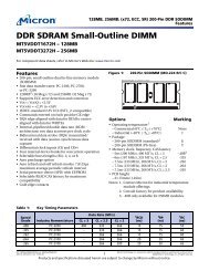
1GB, 2GB, 4GB 184-PIN DDR SDRAM RDIMM - Micron
1GB, 2GB, 4GB 184-PIN DDR SDRAM RDIMM - Micron
1GB, 2GB, 4GB 184-PIN DDR SDRAM RDIMM - Micron

You also want an ePaper? Increase the reach of your titles
YUMPU automatically turns print PDFs into web optimized ePapers that Google loves.
<strong>DDR</strong> <strong>SDRAM</strong><br />
REGISTERED DIMM<br />
Features<br />
• <strong>184</strong>-pin, dual in-line memory modules (DIMM)<br />
Fast data transfer rates: PC1600, PC2100, and<br />
PC2700<br />
Utilizes 200 MT/s, 266 MT/s, and 333 MT/s <strong>DDR</strong><br />
<strong>SDRAM</strong> stacked components<br />
Supports ECC error detection and correction<br />
Registered inputs with one-clock delay<br />
Phase-lock loop (PLL) clock driver to reduce loading<br />
<strong>1GB</strong> (128 Meg x 72), <strong>2GB</strong> (256 Meg x 72), and <strong>4GB</strong><br />
(512 Meg x 72)<br />
VDD= VDDQ = +2.5V<br />
VDDSPD = +2.3V to +3.6V<br />
2.5V I/O (SSTL_2 compatible)<br />
Commands entered on each positive CK edge<br />
DQS edge-aligned with data for READs; centeraligned<br />
with data for WRITEs<br />
Internal, pipelined double data rate (<strong>DDR</strong>)<br />
architecture; two data accesses per clock cycle<br />
Bidirectional data strobe (DQS) transmitted/<br />
received with data, i.e., source-synchronous data<br />
capture<br />
Differential clock inputs (CK and CK#)<br />
Four internal device banks for concurrent operation<br />
Selectable burst lengths: 2, 4, or 8<br />
Auto Refresh and Self Refresh Modes<br />
7.8125µs maximum average periodic refresh<br />
interval<br />
Serial Presence Detect (SPD) with EEPROM<br />
Selectable READ CAS latency<br />
Gold edge contacts<br />
<strong>1GB</strong>, <strong>2GB</strong>, <strong>4GB</strong> (x72, ECC, PLL, DR)<br />
<strong>184</strong>-<strong>PIN</strong> <strong>DDR</strong> <strong>SDRAM</strong> <strong>RDIMM</strong><br />
MT36VDDT12872 – <strong>1GB</strong><br />
MT36VDDT25672 – <strong>2GB</strong><br />
MT36VDDT51272 – <strong>4GB</strong><br />
For the latest data sheet, please refer to the <strong>Micron</strong> ® Web<br />
site: www.micron.com/products/modules<br />
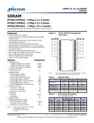
Figure 1: <strong>184</strong>-Pin DIMM (MO-206)<br />
Standard PCB (1.7in./43.18mm)<br />
Low Profile PCB (1.2in./30.48mm)<br />
OPTIONS MARKING<br />
Package<br />
<strong>184</strong>-pin DIMM (Standard) G<br />
<strong>184</strong>-pin DIMM (Lead-free) 1 Y<br />
Memory Clock, Speed, CAS Latency 2<br />
6ns (167 Mhz), 333 MT/s, CL = 2.5 -335<br />
7.5ns (133 Mhz), 266 MT/s, CL = 2 -262 1<br />
7.5ns (133 Mhz), 266 MT/s, CL = 2 -26A 1<br />
7.5ns (133 Mhz), 266 MT/s, CL = 2.5 -265<br />
10ns (100 Mhz), 200 MT/s, CL = 2 -202<br />
Standard 1.7in. (43.18mm) See note, page 2<br />
Low Profile 1.2in. (30.48mm) See note, page 2<br />
NOTE: 1. Contact <strong>Micron</strong> for product availability.<br />
2. CL = Device CAS (READ) Latency; registered<br />
mode adds one clock cycle to CL.<br />
pdf: 09005aef815aa78c, source: 09005aef807da325<br />
DD36C128_256_512x72G.fm - Rev. E 10/04 EN 1 ©2004 <strong>Micron</strong> Technology, Inc. All rights reserved.<br />
PRODUCTS AND SPECIFICATIONS DISCUSSED HEREIN ARE SUBJECT TO CHANGE BY MICRON WITHOUT NOTICE.<br />
PCB
Table 1: Address Table<br />
<strong>1GB</strong>, <strong>2GB</strong>, <strong>4GB</strong> (x72, ECC, PLL, DR)<br />
<strong>184</strong>-<strong>PIN</strong> <strong>DDR</strong> <strong>SDRAM</strong> <strong>RDIMM</strong><br />
<strong>1GB</strong> <strong>2GB</strong> <strong>4GB</strong><br />
Refresh Count 8K 8K 8K<br />
Row Addressing 8K (A0–A12) 8K (A0–A12) 16K (A0–A13)<br />
Device Bank Addressing 4 (BA0, BA1) 4 (BA0, BA1) 4 (BA0, BA1)<br />
Base Device Configuration 256Mb (64 Megx 4) 512Mb (128 Meg x 4) 1Gb (256 Meg x 4)<br />
Column Addressing 2K (A0–A9, A11) 4K (A0–A9, A11, A12) 4K (A0–A9, A11, A12)<br />
Module Rank Addressing 2 (S0#, S1#) 2 (S0#, S1#) 2 (S0#, S1#)<br />
Table 2: Part Numbers and Timing Parameters<br />
PART NUMBER 1<br />
MODULE<br />
DENSITY CONFIGURATION MODULE<br />
BANDWIDTH<br />
MEMORY CLOCK,<br />
DATA RATE<br />
LATENCY<br />
(CL - tRCD - tRP) MT36VDDT12872G-335__ <strong>1GB</strong> 128 Meg x 72 2.7 GB/s 6ns/333 MT/s 2.5-3-3<br />
MT36VDDT12872Y-335__ <strong>1GB</strong> 128 Meg x 72 2.7 GB/s 6ns/333 MT/s 2.5-3-3<br />
MT36VDDT12872G-262__ <strong>1GB</strong> 128 Meg x 72 2.1 GB/s 7.5ns, 266 MT/s 2-2-2<br />
MT36VDDT12872Y-262__ <strong>1GB</strong> 128 Meg x 72 2.1 GB/s 7.5ns, 266 MT/s 2-2-2<br />
MT36VDDT12872G-26A__ <strong>1GB</strong> 128 Meg x 72 2.1 GB/s 7.5ns, 266 MT/s 2-3-3<br />
MT36VDDT12872Y-26A__ <strong>1GB</strong> 128 Meg x 72 2.1 GB/s 7.5ns, 266 MT/s 2-3-3<br />
MT36VDDT12872G-265__ <strong>1GB</strong> 128 Meg x 72 2.1 GB/s 7.5ns, 266 MT/s 2.5-3-3<br />
MT36VDDT12872Y-265__ <strong>1GB</strong> 128 Meg x 72 2.1 GB/s 7.5ns, 266 MT/s 2.5-3-3<br />
MT36VDDT12872G-202__ <strong>1GB</strong> 128 Meg x 72 1.6 GB/s 10ns, 200 MT/s 2-2-2<br />
MT36VDDT12872Y-202__ <strong>1GB</strong> 128 Meg x 72 1.6 GB/s 10ns, 200 MT/s 2-2-2<br />
MT36VDDT25672G-335__ <strong>2GB</strong> 256 Meg x 72 2.7 GB/s 6ns/333 MT/s 2.5-3-3<br />
MT36VDDT25672Y-335__ <strong>2GB</strong> 256 Meg x 72 2.7 GB/s 6ns/333 MT/s 2.5-3-3<br />
MT36VDDT25672G-262__ <strong>2GB</strong> 256 Meg x 72 2.1 GB/s 7.5ns, 266 MT/s 2-2-2<br />
MT36VDDT25672Y-262__ <strong>2GB</strong> 256 Meg x 72 2.1 GB/s 7.5ns, 266 MT/s 2-2-2<br />
MT36VDDT25672G-26A__ <strong>2GB</strong> 256 Meg x 72 2.1 GB/s 7.5ns, 266 MT/s 2-3-3<br />
MT36VDDT25672Y-26A__ <strong>2GB</strong> 256 Meg x 72 2.1 GB/s 7.5ns, 266 MT/s 2-3-3<br />
MT36VDDT25672G-265__ <strong>2GB</strong> 256 Meg x 72 2.1 GB/s 7.5ns, 266 MT/s 2.5-3-3<br />
MT36VDDT25672Y-265__ <strong>2GB</strong> 256 Meg x 72 2.1 GB/s 7.5ns, 266 MT/s 2.5-3-3<br />
MT36VDDT25672G-202__ <strong>2GB</strong> 256 Meg x 72 1.6 GB/s 10ns, 200 MT/s 2-2-2<br />
MT36VDDT25672Y-202__ <strong>2GB</strong> 256 Meg x 72 1.6 GB/s 10ns, 200 MT/s 2-2-2<br />
MT36VDDT51272G-335__ <strong>4GB</strong> 512 Meg x 72 2.7 GB/s 6ns/333 MT/s 2.5-3-3<br />
MT36VDDT51272Y-335__ <strong>4GB</strong> 512 Meg x 72 2.7 GB/s 6ns/333 MT/s 2.5-3-3<br />
MT36VDDT51272G-262__2 <strong>4GB</strong> 512 Meg x 72 2.1 GB/s 7.5ns, 266 MT/s 2-2-2<br />
MT36VDDT51272Y-262__2 <strong>4GB</strong> 512 Meg x 72 2.1 GB/s 7.5ns, 266 MT/s 2-2-2<br />
MT36VDDT51272G-26A__2 <strong>4GB</strong> 512 Meg x 72 2.1 GB/s 7.5ns, 266 MT/s 2-3-3<br />
MT36VDDT51272Y-26A__2 <strong>4GB</strong> 512 Meg x 72 2.1 GB/s 7.5ns, 266 MT/s 2-3-3<br />
MT36VDDT51272G-265__2 <strong>4GB</strong> 512 Meg x 72 2.1 GB/s 7.5ns, 266 MT/s 2.5-3-3<br />
MT36VDDT51272Y-265__2 <strong>4GB</strong> 512 Meg x 72 2.1 GB/s 7.5ns, 266 MT/s 2.5-3-3<br />
MT36VDDT51272G-202__2 <strong>4GB</strong> 512 Meg x 72 1.6 GB/s 10ns, 200 MT/s 2-2-2<br />
MT36VDDT51272Y-202__2 <strong>4GB</strong> 512 Meg x 72 1.6 GB/s 10ns, 200 MT/s 2-2-2<br />
NOTE:<br />
1. All part numbers end with a two-place code (not shown), designating component and PCB revisions. Consult factory for<br />
current revision codes. Example: MT36VDDT12872G-265A1.<br />
2. Contact <strong>Micron</strong> for product availability.<br />
pdf: 09005aef815aa78c, source: 09005aef807da325 <strong>Micron</strong> Technology, Inc., reserves the right to change products or specifications without notice.<br />
DD36C128_256_512x72G.fm - Rev. E 10/04 EN 2 ©2004 <strong>Micron</strong> Technology, Inc. All rights reserved.
Table 3: Pin Assignment<br />
(<strong>184</strong>-Pin DIMM Front)<br />
<strong>PIN</strong> SYMBOL <strong>PIN</strong> SYMBOL <strong>PIN</strong> SYMBOL <strong>PIN</strong> SYMBOL<br />
1 VREF 24 DQ17 47 DQS8 70 VDD<br />
2 DQ0 25 DQS2 48 A0 71 NC<br />
3 VSS 26 VSS 49 CB2 72 DQ48<br />
4 DQ1 27 A9 50 VSS 73 DQ49<br />
5 DQS0 28 DQ18 51 CB3 74 VSS<br />
6 DQ2 29 A7 52 BA1 75 DNU<br />
7 VDD 30 VDDQ 53 DQ32 76 DNU<br />
8 DQ3 31 DQ19 54 VDDQ 77 VDDQ<br />
9 NC 32 A5 55 DQ33 78 DQS6<br />
10 RESET# 33 DQ24 56 DQS4 79 DQ50<br />
11 VSS 34 VSS 57 DQ34 80 DQ51<br />
12 DQ8 35 DQ25 58 VSS 81 VSS<br />
13 DQ9 36 DQS3 59 BA0 82 NC<br />
14 DQS1 37 A4 60 DQ35 83 DQ56<br />
15 VDDQ 38 VDD 61 DQ40 84 DQ57<br />
16 DNU 39 DQ26 62 VDDQ 85 VDD<br />
17 DNU 40 DQ27 63 WE# 86 DQS7<br />
18 VSS 41 A2 64 DQ41 87 DQ58<br />
19 DQ10 42 VSS 65 CAS# 88 DQ59<br />
20 DQ11 43 A1 66 VSS 89 VSS<br />
21 CKE0 44 CB0 67 DQS5 90 DNU<br />
22 VDDQ 45 CB1 68 DQ42 91 SDA<br />
23 DQ16 46 VDD 69 DQ43 92 SCL<br />
NOTE:<br />
1. Pin 167 is NC for <strong>1GB</strong> and <strong>2GB</strong> modules, A13 for <strong>4GB</strong> module.<br />
Front View<br />
U1 U2 U3 U4 U5<br />
Back View<br />
Standard PCB<br />
U11<br />
U12<br />
Figure 2: <strong>184</strong>-Pin DIMM Pin Locations<br />
U6 U7 U8 U9 U10<br />
U14 U15 U16 U17 U18 U19 U20 U21 U22<br />
U13<br />
<strong>1GB</strong>, <strong>2GB</strong>, <strong>4GB</strong> (x72, ECC, PLL, DR)<br />
<strong>184</strong>-<strong>PIN</strong> <strong>DDR</strong> <strong>SDRAM</strong> <strong>RDIMM</strong><br />
Table 4: Pin Assignment<br />
(<strong>184</strong>-Pin DIMM Back)<br />
<strong>PIN</strong> SYMBOL <strong>PIN</strong> SYMBOL <strong>PIN</strong> SYMBOL <strong>PIN</strong> SYMBOL<br />
93 VSS 116 VSS 139 VSS 162 DQ47<br />
94 DQ4 117 DQ21 140 DQS17 163 NC<br />
95 DQ5 118 A11 141 A10 164 VDDQ<br />
96 VDDQ 119 DQS11 142 CB6 165 DQ52<br />
97 DQS9 120 VDD 143 VDDQ 166 DQ53<br />
98 DQ6 121 DQ22 144 CB7 167 NC/A13<br />
99 DQ7 122 A8 145 VSS 168 VDD<br />
100 VSS 123 DQ23 146 DQ36 169 DQS15<br />
101 NC 124 VSS 147 DQ37 170 DQ54<br />
102 NC 125 A6 148 VDD 171 DQ55<br />
103 NC 126 DQ28 149 DQS13 172 VDDQ<br />
104 VDDQ 127 DQ29 150 DQ38 173 NC<br />
105 DQ12 128 VDDQ 151 DQ39 174 DQ60<br />
106 DQ13 129 DQS12 152 VSS 175 DQ61<br />
107 DQS10 130 A3 153 DQ44 176 VSS<br />
108 VDD 131 DQ30 154 RAS# 177 DQS16<br />
109 DQ14 132 VSS 155 DQ45 178 DQ62<br />
110 DQ15 133 DQ31 156 VDDQ 179 DQ63<br />
111 CKE1 134 CB4 157 S0# 180 VDDQ<br />
112 VDDQ 135 CB5 158 S1# 181 SA0<br />
113 NC 136 VDDQ 159 DQS14 182 SA1<br />
114 DQ20 137 CK0 160 VSS 183 SA2<br />
115 A12 138 CK0# 161 DQ46 <strong>184</strong> VDDSPD<br />
Front View<br />
U1 U2 U3 U4<br />
Low Profile PCB<br />
pdf: 09005aef815aa78c, source: 09005aef807da325 <strong>Micron</strong> Technology, Inc., reserves the right to change products or specifications without notice.<br />
DD36C128_256_512x72G.fm - Rev. E 10/04 EN 3 ©2004 <strong>Micron</strong> Technology, Inc. All rights reserved.<br />
U19<br />
U20<br />
U10 U11 U12 U13 U14<br />
U5 U6 U7 U8 U9<br />
<strong>PIN</strong> 1 <strong>PIN</strong> 52 <strong>PIN</strong> 53 <strong>PIN</strong> 92 <strong>PIN</strong> 1 <strong>PIN</strong> 52 <strong>PIN</strong> 53 <strong>PIN</strong> 92<br />
Back View<br />
U21<br />
U22<br />
U15 U16 U17 U18<br />
<strong>PIN</strong> <strong>184</strong> <strong>PIN</strong> 145<br />
<strong>PIN</strong> 144<br />
<strong>PIN</strong> 93<br />
<strong>PIN</strong> <strong>184</strong><br />
<strong>PIN</strong> 145<br />
<strong>PIN</strong> 144<br />
<strong>PIN</strong> 93<br />
Indicates a VDD or VDDQ pin Indicates a VSS pin Indicates a VDD or VDDQ pin Indicates a VSS pin
<strong>1GB</strong>, <strong>2GB</strong>, <strong>4GB</strong> (x72, ECC, PLL, DR)<br />
<strong>184</strong>-<strong>PIN</strong> <strong>DDR</strong> <strong>SDRAM</strong> <strong>RDIMM</strong><br />
Table 5: Pin Descriptions<br />
Pin numbers may not necessarily correlate with symbols. Refer to Pin Assignment tables on page 3 for more information<br />
<strong>PIN</strong> NUMBERS SYMBOL TYPE DESCRIPTION<br />
63, 65, 154 WE#, CAS#, Input Command Inputs: RAS#, CAS#, and WE# define the command<br />
being entered.<br />
137, 138 CK0, CK0# Input Clock: CK and CK# are differential clock inputs. All address and<br />
control input signals are sampled on the crossing of the positive<br />
edge of CK and negative edge of CK#. Output data (DQ and DQS)<br />
is referenced to the crossings of CK and CK#.<br />
21, 111 CKE0, CKE1 Input Clock Enable: CKE HIGH activates and CKE LOW deactivates the<br />
internal clock, input buffers, and output drivers. Taking CKE LOW<br />
provides PRECHARGE POWER-DOWN and SELF REFRESH<br />
operations (all device banks idle), or ACTIVE POWER-DOWN (row<br />
ACTIVE in any device bank). CKE is synchronous for POWER-<br />
DOWN entry and exit, and for SELF REFRESH entry. CKE is<br />
asynchronous for SELF REFRESH exit and for disabling the outputs.<br />
CKE must be maintained HIGH throughout read and write<br />
accesses. Input buffers (excluding CK, CK#, and CKE) are disabled<br />
during POWER-DOWN. Input buffers (excluding CKE) are disabled<br />
during SELF REFRESH. CKE is an SSTL_2 input but will detect an<br />
LVCMOS LOW level after VDD is applied and until CKE is first<br />
brought HIGH. After CKE is brought HIGH, it becomes an SSTL_2<br />
input only.<br />
157, 158 S0#, S1# Input Chip Select: S# enables (registered LOW) and disables (registered<br />
HIGH) the command decoder. All commands are masked when S#<br />
is registered HIGH. S# is considered part of the command code.<br />
52, 59 BA0, BA1 Input Bank Address: BA0 and BA1 define to which device bank an<br />
ACTIVE, READ, WRITE, or PRECHARGE command is being applied.<br />
27, 29, 32, 37, 41, 43, 48,<br />
115, 118, 122, 125, 130,<br />
141, 167 (<strong>4GB</strong>)<br />
A0–A12<br />
(<strong>1GB</strong>, <strong>2GB</strong>)<br />
A0–A13<br />
(<strong>4GB</strong>)<br />
Input Address Inputs: Provide the row address for ACTIVE commands,<br />
and the column address and auto precharge bit (A10) for READ/<br />
WRITE commands, to select one location out of the memory array<br />
in the respective device bank. A10 sampled during a PRECHARGE<br />
command determines whether the PRECHARGE applies to one<br />
device bank (A10 LOW, device bank selected by BA0, BA1) or all<br />
device banks (A10 HIGH). The address inputs also provide the opcode<br />
during a MODE REGISTER SET command. BA0 and BA1<br />
define which mode register (mode register or extended mode<br />
register) is loaded during the LOAD MODE REGISTER command.<br />
10 RESET# Input Asynchronously forces all register outputs LOW when RESET# is<br />
LOW. This signal can be used during power- up to ensure CKE is<br />
LOW and <strong>SDRAM</strong> DQs are High-Z.<br />
91 SDA Input/<br />
Output<br />
Serial Presence-Detect Data: SDA is a bidirectional pin used to<br />
transfer addresses and data into and out of the presence-detect<br />
portion of the module.<br />
92 SCL Input Serial Clock for Presence-Detect: SCL is used to synchronize the<br />
presence-detect data transfer to and from the module.<br />
181, 182, 183 SA0–SA2 Input Presence-Detect Address Inputs: These pins are used to configure<br />
the presence-detect device.<br />
44, 45, 49, 51, 134, 135, 142,<br />
144<br />
5, 14, 25, 36, 47, 56, 67, 78,<br />
86, 97, 107, 119, 129, 140,<br />
149, 159, 169, 177<br />
CB0–CB7 Input/<br />
Output<br />
DQS0–DQS17 Input/<br />
Output<br />
Check bits.<br />
Data Strobe: Output with READ data, input with WRITE data. DQS<br />
is edge-aligned with READ data, centered in WRITE data. Used to<br />
capture data.<br />
pdf: 09005aef815aa78c, source: 09005aef807da325 <strong>Micron</strong> Technology, Inc., reserves the right to change products or specifications without notice.<br />
DD36C128_256_512x72G.fm - Rev. E 10/04 EN 4 ©2004 <strong>Micron</strong> Technology, Inc. All rights reserved.
2, 4, 6, 8, 12, 13, 19, 20, 23,<br />
24, 28, 31, 33, 35, 39, 40, 53,<br />
55, 57, 60, 61, 64, 68, 69, 72,<br />
73, 79, 80, 83, 84, 87, 88, 94,<br />
95, 98, 99, 105, 106, 109, 110,<br />
114, 117, 121, 123, 126, 127,<br />
131, 133, 146, 147, 150, 151,<br />
153, 155, 161, 162, 165, 166,<br />
170, 171, 174, 175, 178, 179<br />
DQ0–DQ63 Input/<br />
Output<br />
<strong>1GB</strong>, <strong>2GB</strong>, <strong>4GB</strong> (x72, ECC, PLL, DR)<br />
<strong>184</strong>-<strong>PIN</strong> <strong>DDR</strong> <strong>SDRAM</strong> <strong>RDIMM</strong><br />
Table 5: Pin Descriptions<br />
Pin numbers may not necessarily correlate with symbols. Refer to Pin Assignment tables on page 3 for more information<br />
<strong>PIN</strong> NUMBERS SYMBOL TYPE DESCRIPTION<br />
Data I/Os: Data bus.<br />
1 VREF Supply SSTL_2 reference voltage.<br />
15, 22, 30, 54, 62, 77, 96, 104,<br />
112, 128, 136, 143, 156, 164,<br />
172, 180<br />
VDDQ Supply DQ Power Supply: +2.5V +0.2V.<br />
7, 38, 46, 70, 85, 108, 120,<br />
148, 168<br />
VDD Supply Power Supply:+2.5V +0.2V.<br />
3, 11, 18, 26, 34, 42, 50, 58,<br />
66, 74, 81, 89, 93, 100, 116,<br />
124, 132, 139, 145, 152, 160,<br />
176<br />
VSS Supply Ground.<br />
<strong>184</strong> VDDSPD Supply Serial EEPROM positive power supply: +2.3V to +3.6V.<br />
9, 71, 82, 90, 101, 102, 103,<br />
113, 163, 167 (<strong>1GB</strong>, <strong>2GB</strong>), 173<br />
NC – No Connect: These pins should be left unconnected.<br />
16, 17, 75, 76 DNU – Do Not Use: These pins are not connected on this module but are<br />
assigned pins on other modules in this product family.<br />
pdf: 09005aef815aa78c, source: 09005aef807da325 <strong>Micron</strong> Technology, Inc., reserves the right to change products or specifications without notice.<br />
DD36C128_256_512x72G.fm - Rev. E 10/04 EN 5 ©2004 <strong>Micron</strong> Technology, Inc. All rights reserved.
NOTE:<br />
<strong>1GB</strong>, <strong>2GB</strong>, <strong>4GB</strong> (x72, ECC, PLL, DR)<br />
<strong>184</strong>-<strong>PIN</strong> <strong>DDR</strong> <strong>SDRAM</strong> <strong>RDIMM</strong><br />
Figure 3: Functional Block Diagram (Standard PCB)<br />
DQS0<br />
DQS1<br />
DQS2<br />
DQS3<br />
DQS4<br />
DQS5<br />
DQS6<br />
DQS7<br />
DQS8<br />
S0#, S1#<br />
BA0, BA1<br />
A0-A12 (<strong>1GB</strong>, <strong>2GB</strong>),<br />
A0-A13 (<strong>4GB</strong>)<br />
RAS#<br />
CAS#<br />
CKE0, CKE1<br />
WE#<br />
CK<br />
CK#<br />
DQ0<br />
DQ1<br />
DQ2<br />
DQ3<br />
DQ8<br />
DQ9<br />
DQ10<br />
DQ11<br />
DQ16<br />
DQ17<br />
DQ18<br />
DQ19<br />
DQ24<br />
DQ25<br />
DQ26<br />
DQ27<br />
DQ32<br />
DQ33<br />
DQ34<br />
DQ35<br />
DQ40<br />
DQ41<br />
DQ42<br />
DQ43<br />
DQ48<br />
DQ49<br />
DQ50<br />
DQ51<br />
DQ56<br />
DQ57<br />
DQ58<br />
DQ59<br />
CB0<br />
CB1<br />
CB2<br />
CB3<br />
DQS CS# DM<br />
DQ<br />
DQ U1b<br />
DQ<br />
DQ<br />
DQS CS# DM<br />
DQ<br />
DQ U2b<br />
DQ<br />
DQ<br />
DQS CS# DM<br />
DQ<br />
DQ U3b<br />
DQ<br />
DQ<br />
DQS CS# DM<br />
DQ<br />
DQ U4b<br />
DQ<br />
DQ<br />
DQS CS# DM<br />
DQ<br />
DQ U6b<br />
DQ<br />
DQ<br />
DQS CS# DM<br />
DQ<br />
DQ U7b<br />
DQ<br />
DQ<br />
DQS CS# DM<br />
DQ<br />
DQ U8b<br />
DQ<br />
DQ<br />
DQS CS# DM<br />
DQ<br />
DQ U9b<br />
DQ<br />
DQ<br />
DQS CS# DM<br />
DQ<br />
DQ U5b<br />
DQ<br />
DQ<br />
U11, U13<br />
R<br />
E<br />
G<br />
I<br />
S<br />
T<br />
E<br />
R<br />
S<br />
RS0# VSS<br />
RS1# VSS<br />
RS0# VSS<br />
DQ0<br />
DQ1<br />
DQ2<br />
DQ3<br />
DQ8<br />
DQ9<br />
DQ10<br />
DQ11<br />
DQ16<br />
DQ17<br />
DQ18<br />
DQ19<br />
DQ24<br />
DQ25<br />
DQ26<br />
DQ27<br />
DQ32<br />
DQ33<br />
DQ34<br />
DQ35<br />
DQ40<br />
DQ41<br />
DQ42<br />
DQ43<br />
DQ48<br />
DQ49<br />
DQ50<br />
DQ51<br />
DQ56<br />
DQ57<br />
DQ58<br />
DQ59<br />
CB0<br />
CB1<br />
CB2<br />
CB3<br />
SCL<br />
RS0#, RS1#: <strong>DDR</strong> <strong>SDRAM</strong>s<br />
WP<br />
RBA0, RBA1: <strong>DDR</strong> <strong>SDRAM</strong>s<br />
RA0-RA12 : <strong>DDR</strong> <strong>SDRAM</strong>s<br />
RA0-RA13 : <strong>DDR</strong> <strong>SDRAM</strong>s<br />
RRAS#: <strong>DDR</strong> <strong>SDRAM</strong>s<br />
RCAS#: <strong>DDR</strong> <strong>SDRAM</strong>s<br />
RCKE0, RCKE1: <strong>DDR</strong> <strong>SDRAM</strong>s<br />
RWE#: <strong>DDR</strong> <strong>SDRAM</strong>s<br />
RESET#<br />
DQS CS# DM<br />
DQ<br />
DQ U1t<br />
DQ<br />
DQ<br />
DQS CS# DM<br />
DQ<br />
DQ U2t<br />
DQ<br />
DQ<br />
DQS CS# DM<br />
DQ<br />
DQ U3t<br />
DQ<br />
DQ<br />
DQS CS# DM<br />
DQ<br />
DQ U4t<br />
DQ<br />
DQ<br />
DQS CS# DM<br />
DQ<br />
DQ U6t<br />
DQ<br />
DQ<br />
DQS CS# DM<br />
DQ<br />
DQ U7t<br />
DQ<br />
DQ<br />
DQS CS# DM<br />
DQ<br />
DQ U8t<br />
DQ<br />
DQ<br />
DQS CS# DM<br />
DQ<br />
DQ U9t<br />
DQ<br />
DQ<br />
DQS CS# DM<br />
DQ<br />
DQ U5t<br />
DQ<br />
DQ<br />
1. All resistor values are 22Ω unless otherwise specified.<br />
2. 'b' = bottom portion of stacked <strong>SDRAM</strong>, 't' = top portion of stacked<br />
<strong>SDRAM</strong>.<br />
3. Per industry standard, <strong>Micron</strong> modules utilize various component speed<br />
grades, as referenced in the module part numbering guide at<br />
www.micron.com/numberguide.<br />
DQS CS# DM<br />
DQ<br />
DQ U22b<br />
DQ<br />
DQ<br />
pdf: 09005aef815aa78c, source: 09005aef807da325 <strong>Micron</strong> Technology, Inc., reserves the right to change products or specifications without notice.<br />
DD36C128_256_512x72G.fm - Rev. E 10/04 EN 6 ©2004 <strong>Micron</strong> Technology, Inc. All rights reserved.<br />
DQS9<br />
DQS10<br />
DQS11<br />
DQS12<br />
DQS13<br />
DQS14<br />
DQS15<br />
DQS16<br />
DQS17<br />
DQ4<br />
DQ5<br />
DQ6<br />
DQ7<br />
DQ12<br />
DQ13<br />
DQ14<br />
DQ15<br />
DQ20<br />
DQ21<br />
DQ22<br />
DQ23<br />
DQ28<br />
DQ29<br />
DQ30<br />
DQ31<br />
DQ36<br />
DQ37<br />
DQ38<br />
DQ39<br />
DQ44<br />
DQ45<br />
DQ46<br />
DQ47<br />
DQ52<br />
DQ53<br />
DQ54<br />
DQ55<br />
DQ60<br />
DQ61<br />
DQ62<br />
DQ63<br />
CB4<br />
CB5<br />
CB6<br />
CB7<br />
SERIAL PD<br />
U10<br />
A0 A1 A2<br />
SA0 SA1 SA2<br />
VREF<br />
VSS<br />
DQS CS# DM<br />
DQ<br />
DQ U21b<br />
DQ<br />
DQ<br />
DQS CS# DM<br />
DQ<br />
DQ U20b<br />
DQ<br />
DQ<br />
DQS CS# DM<br />
DQ<br />
DQ U19b<br />
DQ<br />
DQ<br />
DQS CS# DM<br />
DQ<br />
DQ U17b<br />
DQ<br />
DQ<br />
DQS CS# DM<br />
DQ<br />
DQ U16b<br />
DQ<br />
DQ<br />
DQS CS# DM<br />
DQ<br />
DQ U15b<br />
DQ<br />
DQ<br />
DQS CS# DM<br />
DQ<br />
DQ U14b<br />
DQ<br />
DQ<br />
DQS CS# DM<br />
DQ<br />
DQ U18b<br />
DQ<br />
DQ<br />
SDA<br />
CK0<br />
CK0#<br />
DQ4<br />
DQ5<br />
DQ6<br />
DQ7<br />
DQ12<br />
DQ13<br />
DQ14<br />
DQ15<br />
DQ20<br />
DQ21<br />
DQ22<br />
DQ23<br />
DQ28<br />
DQ29<br />
DQ30<br />
DQ31<br />
DQ36<br />
DQ37<br />
DQ38<br />
DQ39<br />
DQ44<br />
DQ45<br />
DQ46<br />
DQ47<br />
DQ52<br />
DQ53<br />
DQ54<br />
DQ55<br />
DQ60<br />
DQ61<br />
DQ62<br />
DQ63<br />
CB4<br />
CB5<br />
CB6<br />
CB7<br />
PLL<br />
U12<br />
VDDSPD SPD<br />
VDDQ<br />
<strong>DDR</strong> <strong>SDRAM</strong>S<br />
VDD <strong>DDR</strong> <strong>SDRAM</strong>S<br />
<strong>DDR</strong> <strong>SDRAM</strong>S<br />
<strong>DDR</strong> <strong>SDRAM</strong>S<br />
RS1# VSS<br />
DQS CS# DM<br />
DQ<br />
DQ U22t<br />
DQ<br />
DQ<br />
DQS CS# DM<br />
DQ<br />
DQ U21t<br />
DQ<br />
DQ<br />
DQS CS# DM<br />
DQ<br />
DQ U20t<br />
DQ<br />
DQ<br />
DQS CS# DM<br />
DQ<br />
DQ U19t<br />
DQ<br />
DQ<br />
DQS CS# DM<br />
DQ<br />
DQ U17t<br />
DQ<br />
DQ<br />
DQS CS# DM<br />
DQ<br />
DQ U16t<br />
DQ<br />
DQ<br />
DQS CS# DM<br />
DQ<br />
DQ U15t<br />
DQ<br />
DQ<br />
DQS CS# DM<br />
DQ<br />
DQ U14t<br />
DQ<br />
DQ<br />
DQS CS# DM<br />
DQ<br />
DQ U18t<br />
DQ<br />
DQ<br />
<strong>DDR</strong> <strong>SDRAM</strong> X 4<br />
<strong>DDR</strong> <strong>SDRAM</strong> X 4<br />
<strong>DDR</strong> <strong>SDRAM</strong> X 4<br />
<strong>DDR</strong> <strong>SDRAM</strong> X 4<br />
<strong>DDR</strong> <strong>SDRAM</strong> X 4<br />
<strong>DDR</strong> <strong>SDRAM</strong> X 4<br />
<strong>DDR</strong> <strong>SDRAM</strong> X 4<br />
<strong>DDR</strong> <strong>SDRAM</strong> X 4<br />
<strong>DDR</strong> <strong>SDRAM</strong> X 4<br />
REGISTER X 2<br />
Standard modules use the following <strong>DDR</strong> <strong>SDRAM</strong> devices:<br />
MT46V64M4TG (<strong>1GB</strong>); MT46V128M4TG (<strong>2GB</strong>); MT46V256M4TG (<strong>4GB</strong>)<br />
Lead-free modules use the following <strong>DDR</strong> <strong>SDRAM</strong> devices:<br />
MT46V64M4P (<strong>1GB</strong>); MT46V128M4P (<strong>2GB</strong>); MT46V256M4P (<strong>4GB</strong>)
NOTE:<br />
S0#, S1#<br />
BA0, BA1<br />
A0-A12 (<strong>1GB</strong>, <strong>2GB</strong>),<br />
A0-A13 (<strong>4GB</strong>)<br />
RAS#<br />
CAS#<br />
CKE0, CKE1<br />
WE#<br />
<strong>1GB</strong>, <strong>2GB</strong>, <strong>4GB</strong> (x72, ECC, PLL, DR)<br />
<strong>184</strong>-<strong>PIN</strong> <strong>DDR</strong> <strong>SDRAM</strong> <strong>RDIMM</strong><br />
Figure 4: Functional Block Diagram (Low-Profile PCB)<br />
CK<br />
CK#<br />
DQS0<br />
DQS1<br />
DQS2<br />
DQS3<br />
DQS4<br />
DQS5<br />
DQS6<br />
DQS7<br />
DQS8<br />
DQ0<br />
DQ1<br />
DQ2<br />
DQ3<br />
DQ8<br />
DQ9<br />
DQ10<br />
DQ11<br />
DQ16<br />
DQ17<br />
DQ18<br />
DQ19<br />
DQ24<br />
DQ25<br />
DQ26<br />
DQ27<br />
DQ32<br />
DQ33<br />
DQ34<br />
DQ35<br />
DQ40<br />
DQ41<br />
DQ42<br />
DQ43<br />
DQ48<br />
DQ49<br />
DQ50<br />
DQ51<br />
DQ56<br />
DQ57<br />
DQ58<br />
DQ59<br />
CB0<br />
CB1<br />
CB2<br />
CB3<br />
U19, U21<br />
RS0# VSS<br />
RS1# VSS<br />
RS0# VSS<br />
DQS CS# DM<br />
DQ<br />
DQ U1b<br />
DQ<br />
DQ<br />
DQS CS# DM<br />
DQ<br />
DQ U2b<br />
DQ<br />
DQ<br />
DQS CS# DM<br />
DQ<br />
DQ U3b<br />
DQ<br />
DQ<br />
DQS CS# DM<br />
DQ<br />
DQ U4b<br />
DQ<br />
DQ<br />
DQS CS# DM<br />
DQ<br />
DQ U6b<br />
DQ<br />
DQ<br />
DQS CS# DM<br />
DQ<br />
DQ U7b<br />
DQ<br />
DQ<br />
DQS CS# DM<br />
DQ<br />
DQ U8b<br />
DQ<br />
DQ<br />
DQS CS# DM<br />
DQ<br />
DQ U9b<br />
DQ<br />
DQ<br />
DQS CS# DM<br />
DQ<br />
DQ U5b<br />
DQ<br />
DQ<br />
DQ0<br />
DQ1<br />
DQ2<br />
DQ3<br />
DQ8<br />
DQ9<br />
DQ10<br />
DQ11<br />
DQ16<br />
DQ17<br />
DQ18<br />
DQ19<br />
DQ24<br />
DQ25<br />
DQ26<br />
DQ27<br />
DQ32<br />
DQ33<br />
DQ34<br />
DQ35<br />
DQ40<br />
DQ41<br />
DQ42<br />
DQ43<br />
DQ48<br />
DQ49<br />
DQ50<br />
DQ51<br />
DQ56<br />
DQ57<br />
DQ58<br />
DQ59<br />
CB0<br />
CB1<br />
CB2<br />
CB3<br />
DQS CS# DM<br />
DQ<br />
DQ U1t<br />
DQ<br />
DQ<br />
DQS CS# DM<br />
DQ<br />
DQ U2t<br />
DQ<br />
DQ<br />
DQS CS# DM<br />
DQ<br />
DQ U3t<br />
DQ<br />
DQ<br />
DQS CS# DM<br />
DQ<br />
DQ U4t<br />
DQ<br />
DQ<br />
DQS CS# DM<br />
DQ<br />
DQ U6t<br />
DQ<br />
DQ<br />
DQS CS# DM<br />
DQ<br />
DQ U7t<br />
DQ<br />
DQ<br />
DQS CS# DM<br />
DQ<br />
DQ U8t<br />
DQ<br />
DQ<br />
DQS CS# DM<br />
DQ<br />
DQ U9t<br />
DQ<br />
DQ<br />
DQS CS# DM<br />
DQ<br />
DQ U5t<br />
DQ<br />
DQ<br />
1. All resistor values are 22Ω unless otherwise specified.<br />
2. 'b' = bottom portion of stacked <strong>SDRAM</strong>, 't' = top portion of stacked<br />
<strong>SDRAM</strong>.<br />
3. Per industry standard, <strong>Micron</strong> modules utilize various component speed<br />
grades, as referenced in the module part numbering guide at<br />
www.micron.com/numberguide.<br />
R<br />
E<br />
G<br />
I<br />
S<br />
T<br />
E<br />
R<br />
S<br />
DQS CS# DM<br />
DQ<br />
DQ U18b<br />
DQ<br />
DQ<br />
pdf: 09005aef815aa78c, source: 09005aef807da325 <strong>Micron</strong> Technology, Inc., reserves the right to change products or specifications without notice.<br />
DD36C128_256_512x72G.fm - Rev. E 10/04 EN 7 ©2004 <strong>Micron</strong> Technology, Inc. All rights reserved.<br />
DQS9<br />
DQS10<br />
DQS11<br />
DQS12<br />
DQS13<br />
DQS14<br />
DQS15<br />
DQS16<br />
DQS17<br />
DQ4<br />
DQ5<br />
DQ6<br />
DQ7<br />
DQ12<br />
DQ13<br />
DQ14<br />
DQ15<br />
DQ20<br />
DQ21<br />
DQ22<br />
DQ23<br />
DQ28<br />
DQ29<br />
DQ30<br />
DQ31<br />
DQ36<br />
DQ37<br />
DQ38<br />
DQ39<br />
DQ44<br />
DQ45<br />
DQ46<br />
DQ47<br />
DQ52<br />
DQ53<br />
DQ54<br />
DQ55<br />
DQ60<br />
DQ61<br />
DQ62<br />
DQ63<br />
CB4<br />
CB5<br />
CB6<br />
CB7<br />
DQS CS# DM<br />
DQ<br />
DQ U17b<br />
DQ<br />
DQ<br />
DQS CS# DM<br />
DQ<br />
DQ U16b<br />
DQ<br />
DQ<br />
DQS CS# DM<br />
DQ<br />
DQ U15b<br />
DQ<br />
DQ<br />
DQS CS# DM<br />
DQ<br />
DQ U13b<br />
DQ<br />
DQ<br />
DQS CS# DM<br />
DQ<br />
DQ U12b<br />
DQ<br />
DQ<br />
DQS CS# DM<br />
DQ<br />
DQ U11b<br />
DQ<br />
DQ<br />
DQS CS# DM<br />
DQ<br />
DQ U10b<br />
DQ<br />
DQ<br />
DQS CS# DM<br />
DQ<br />
DQ U14b<br />
DQ<br />
DQ<br />
DQ4<br />
DQ5<br />
DQ6<br />
DQ7<br />
DQ12<br />
DQ13<br />
DQ14<br />
DQ15<br />
DQ20<br />
DQ21<br />
DQ22<br />
DQ23<br />
DQ28<br />
DQ29<br />
DQ30<br />
DQ31<br />
DQ36<br />
DQ37<br />
DQ38<br />
DQ39<br />
DQ44<br />
DQ45<br />
DQ46<br />
DQ47<br />
DQ52<br />
DQ53<br />
DQ54<br />
DQ55<br />
DQ60<br />
DQ61<br />
DQ62<br />
DQ63<br />
CB4<br />
CB5<br />
CB6<br />
CB7<br />
RS0#, RS1#: <strong>DDR</strong> <strong>SDRAM</strong>s<br />
RBA0, RBA1: <strong>DDR</strong> <strong>SDRAM</strong>s<br />
RA0-RA12 : <strong>DDR</strong> <strong>SDRAM</strong>s<br />
SCL<br />
WP<br />
SERIAL PD<br />
U22<br />
A0 A1 A2<br />
SA0 SA1 SA2<br />
SDA<br />
CK0<br />
CK0#<br />
PLL<br />
U20<br />
RA0-RA13 : <strong>DDR</strong> <strong>SDRAM</strong>s<br />
RRAS#: <strong>DDR</strong> <strong>SDRAM</strong>s<br />
VDDSPD SPD<br />
RCAS#: <strong>DDR</strong> <strong>SDRAM</strong>s<br />
VDDQ<br />
<strong>DDR</strong> <strong>SDRAM</strong>S<br />
RCKE0, RCKE1: <strong>DDR</strong> <strong>SDRAM</strong>s<br />
VDD <strong>DDR</strong> <strong>SDRAM</strong>S<br />
RWE#: <strong>DDR</strong> <strong>SDRAM</strong>s<br />
VREF<br />
<strong>DDR</strong> <strong>SDRAM</strong>S<br />
RESET#<br />
VSS<br />
<strong>DDR</strong> <strong>SDRAM</strong>S<br />
RS1# VSS<br />
DQS CS# DM<br />
DQ<br />
DQ U18t<br />
DQ<br />
DQ<br />
DQS CS# DM<br />
DQ<br />
DQ U17t<br />
DQ<br />
DQ<br />
DQS CS# DM<br />
DQ<br />
DQ U16t<br />
DQ<br />
DQ<br />
DQS CS# DM<br />
DQ<br />
DQ U15t<br />
DQ<br />
DQ<br />
DQS CS# DM<br />
DQ<br />
DQ U13t<br />
DQ<br />
DQ<br />
DQS CS# DM<br />
DQ<br />
DQ U12t<br />
DQ<br />
DQ<br />
DQS CS# DM<br />
DQ<br />
DQ U11t<br />
DQ<br />
DQ<br />
DQS CS# DM<br />
DQ<br />
DQ U10t<br />
DQ<br />
DQ<br />
DQS CS# DM<br />
DQ<br />
DQ U14t<br />
DQ<br />
DQ<br />
<strong>DDR</strong> <strong>SDRAM</strong> X 4<br />
<strong>DDR</strong> <strong>SDRAM</strong> X 4<br />
<strong>DDR</strong> <strong>SDRAM</strong> X 4<br />
<strong>DDR</strong> <strong>SDRAM</strong> X 4<br />
<strong>DDR</strong> <strong>SDRAM</strong> X 4<br />
<strong>DDR</strong> <strong>SDRAM</strong> X 4<br />
<strong>DDR</strong> <strong>SDRAM</strong> X 4<br />
<strong>DDR</strong> <strong>SDRAM</strong> X 4<br />
<strong>DDR</strong> <strong>SDRAM</strong> X 4<br />
REGISTER X 2<br />
Standard modules use the following <strong>DDR</strong> <strong>SDRAM</strong> devices:<br />
MT46V64M4TG (<strong>1GB</strong>); MT46V128M4TG (<strong>2GB</strong>); MT46V256M4TG (<strong>4GB</strong>)<br />
Lead-free modules use the following <strong>DDR</strong> <strong>SDRAM</strong> devices:<br />
MT46V64M4P (<strong>1GB</strong>); MT46V128M4P (<strong>2GB</strong>); MT46V256M4P (<strong>4GB</strong>)
General Description<br />
The MT36VDDT12872, MT36VDDT25672 and<br />
MT36VDDT51272 are high-speed CMOS, dynamic<br />
random-access, <strong>1GB</strong>, <strong>2GB</strong>, and <strong>4GB</strong> registered memory<br />
modules organized in a x72 (ECC) configuration.<br />
<strong>DDR</strong> <strong>SDRAM</strong> modules use internally configured quadbank<br />
<strong>DDR</strong> <strong>SDRAM</strong> devices.<br />
<strong>DDR</strong> <strong>SDRAM</strong> modules use a double data rate architecture<br />
to achieve high-speed operation. Double data<br />
rate architecture is essentially a 2n-prefetch architecture<br />
with an interface designed to transfer two data<br />
words per clock cycle at the I/O pins. A single read or<br />
write access for the <strong>DDR</strong> <strong>SDRAM</strong> module effectively<br />
consists of a single 2n-bit wide, one-clock-cycle data<br />
transfer at the internal DRAM core and two corresponding<br />
n-bit wide, one-half-clock-cycle data transfers<br />
at the I/O pins.<br />
A bidirectional data strobe (DQS) is transmitted<br />
externally, along with data, for use in data capture at<br />
the receiver. DQS is an intermittent strobe transmitted<br />
by <strong>DDR</strong> <strong>SDRAM</strong>s during READs and by the memory<br />
controller during WRITEs. DQS is edge-aligned with<br />
data for READs and center-aligned with data for<br />
WRITEs.<br />
<strong>DDR</strong> <strong>SDRAM</strong> modules operate from a differential<br />
clock (CK and CK#); the crossing of CK going HIGH<br />
and CK# going LOW will be referred to as the positive<br />
edge of CK. Commands (address and control signals)<br />
are registered at every positive edge of CK. Input data<br />
is registered on both edges of DQS, and output data is<br />
referenced to both edges of DQS, as well as to both<br />
edges of CK.<br />
Read and write accesses to <strong>DDR</strong> <strong>SDRAM</strong> modules<br />
are burst oriented; accesses start at a selected location<br />
and continue for a programmed number of locations<br />
in a programmed sequence. Accesses begin with the<br />
registration of an ACTIVE command, which is then followed<br />
by a READ or WRITE command. The address<br />
bits registered coincident with the ACTIVE command<br />
are used to select the device bank and row to be<br />
accessed [BA0, BA1 select device bank, A0–A12 (<strong>1GB</strong>,<br />
<strong>2GB</strong>) or A0–A13 (<strong>4GB</strong>) select device row]. The address<br />
bits registered coincident with the READ or WRITE<br />
command are used to select the device bank and the<br />
starting device column location for the burst access.<br />
<strong>DDR</strong> <strong>SDRAM</strong> modules provide for programmable<br />
read or write burst lengths of 2, 4, or 8 locations. An<br />
auto precharge function may be enabled to provide a<br />
self-timed row precharge that is initiated at the end of<br />
the burst access.<br />
The pipelined, multibank architecture of <strong>DDR</strong><br />
<strong>SDRAM</strong> modules allows for concurrent operation,<br />
<strong>1GB</strong>, <strong>2GB</strong>, <strong>4GB</strong> (x72, ECC, PLL, DR)<br />
<strong>184</strong>-<strong>PIN</strong> <strong>DDR</strong> <strong>SDRAM</strong> <strong>RDIMM</strong><br />
thereby providing high effective bandwidth by hiding<br />
row precharge and activation time.<br />
An auto refresh mode is provided, along with a<br />
power-saving power-down mode. All inputs are compatible<br />
with the JEDEC Standard for SSTL_2. All outputs<br />
are SSTL_2, Class II compatible. For more<br />
information regarding <strong>DDR</strong> <strong>SDRAM</strong> operation, refer to<br />
the 256Mb, 512Mb, or 1Gb <strong>DDR</strong> <strong>SDRAM</strong> component<br />
data sheets.<br />
PLL and Register Operation<br />
<strong>DDR</strong> <strong>SDRAM</strong> modules operate in registered mode<br />
where the control/address input signals are latched in<br />
the register on one rising clock edge and sent to <strong>DDR</strong><br />
<strong>SDRAM</strong> devices on the following rising clock edge<br />
(data access is delayed by one clock). A phase-lock<br />
loop (PLL) on the module is used to redrive the differential<br />
clock signals CK and CK# to <strong>DDR</strong> <strong>SDRAM</strong><br />
devices to minimize system clock loading.<br />
Serial Presence-Detect Operation<br />
<strong>DDR</strong> <strong>SDRAM</strong> modules incorporate serial presencedetect<br />
(SPD). The SPD function is implemented using<br />
a 2,048-bit EEPROM. This nonvolatile storage device<br />
contains 256 bytes. The first 128 bytes can be programmed<br />
by <strong>Micron</strong> to identify the module type and<br />
various <strong>SDRAM</strong> organizations and timing parameters.<br />
The remaining 128 bytes of storage are available for<br />
use by the customer. System READ/WRITE operations<br />
between the master (system logic) and the slave<br />
EEPROM device (DIMM) occur via a standard I 2 C bus<br />
using the DIMM’s SCL (clock) and SDA (data) signals,<br />
together with SA (2:0), which provide eight unique<br />
DIMM/EEPROM addresses. Write protect (WP) is tied<br />
to ground on the module, permanently disabling hardware<br />
write protect.<br />
Mode Register Definition<br />
The mode register is used to define the specific<br />
mode of operation of <strong>DDR</strong> <strong>SDRAM</strong> devices. This definition<br />
includes the selection of a burst length, a burst<br />
type, a CAS latency and an operating mode, as shown<br />
in Figure 5, Mode Register Definition Diagram, on<br />
page 9. The mode register is programmed via the<br />
MODE REGISTER SET command (with BA0 = 0 and<br />
BA1 = 0) and will retain the stored information until it<br />
is programmed again or the device loses power (except<br />
for bit A8, which is self-clearing).<br />
Reprogramming the mode register will not alter the<br />
contents of the memory, provided it is performed correctly.<br />
The mode register must be loaded (reloaded)<br />
when all device banks are idle and no bursts are in<br />
pdf: 09005aef815aa78c, source: 09005aef807da325 <strong>Micron</strong> Technology, Inc., reserves the right to change products or specifications without notice.<br />
DD36C128_256_512x72G.fm - Rev. E 10/04 EN 8 ©2004 <strong>Micron</strong> Technology, Inc. All rights reserved.
progress, and the controller must wait the specified<br />
time before initiating the subsequent operation. Violating<br />
either of these requirements will result in<br />
unspecified operation.<br />
Mode register bits A0–A2 specify the burst length,<br />
A3 specifies the type of burst (sequential or interleaved),<br />
A4–A6 specify the CAS latency, and A7–A12<br />
(<strong>1GB</strong>, <strong>2GB</strong>) or A7–A13 (<strong>4GB</strong>) specify the operating<br />
mode.<br />
Burst Length<br />
Read and write accesses to <strong>DDR</strong> <strong>SDRAM</strong> devices are<br />
burst oriented, with the burst length being programmable,<br />
as shown in Figure 5, Mode Register Definition<br />
Diagram. The burst length determines the maximum<br />
number of column locations that can be accessed for a<br />
given READ or WRITE command. Burst lengths of 2, 4,<br />
or 8 locations are available for both the sequential and<br />
the interleaved burst types.<br />
Reserved states should not be used, as unknown<br />
operation or incompatibility with future versions may<br />
result.<br />
When a READ or WRITE command is issued, a block<br />
of columns equal to the burst length is effectively<br />
selected. All accesses for that burst take place within<br />
this block, meaning that the burst will wrap within the<br />
block if a boundary is reached. The block is uniquely<br />
selected by A1–Ai when the burst length is set to two,<br />
by A2–Ai when the burst length is set to four and by<br />
A3–Ai when the burst length is set to eight (where Ai is<br />
the most significant column address bit for a given<br />
configuration; see Note 5, of Table 6, Burst Definition<br />
Table, on page 10). The remaining (least significant)<br />
address bit(s) is (are) used to select the starting location<br />
within the block. The programmed burst length<br />
applies to both READ and WRITE bursts.<br />
Burst Type<br />
Accesses within a given burst may be programmed<br />
to be either sequential or interleaved; this is referred to<br />
as the burst type and is selected via bit M3.<br />
The ordering of accesses within a burst is determined<br />
by the burst length, the burst type, and the<br />
starting column address, as shown in Table6, Burst<br />
Definition Table, on page 10.<br />
Read Latency<br />
The READ latency is the delay, in clock cycles,<br />
between the registration of a READ command and the<br />
availability of the first bit of output data. The latency<br />
<strong>1GB</strong>, <strong>2GB</strong>, <strong>4GB</strong> (x72, ECC, PLL, DR)<br />
<strong>184</strong>-<strong>PIN</strong> <strong>DDR</strong> <strong>SDRAM</strong> <strong>RDIMM</strong><br />
can be set to 2 or 2.5 clocks, as shown in Figure 6, CAS<br />
Latency Diagram.<br />
Figure 5: Mode Register Definition<br />
Diagram<br />
<strong>1GB</strong>, <strong>2GB</strong> Module Address Bus<br />
BA1 BA0 A12 A11 A10<br />
A9 A8 A7 A6 A5 A4 A3 A2 A1 A0<br />
13 12 11 10 9 8 7 6 5 4 3 2 1 0<br />
0* Operating Mode CAS Latency BT Burst Length<br />
Address Bus<br />
Mode Register (Mx)<br />
pdf: 09005aef815aa78c, source: 09005aef807da325 <strong>Micron</strong> Technology, Inc., reserves the right to change products or specifications without notice.<br />
DD36C128_256_512x72G.fm - Rev. E 10/04 EN 9 ©2004 <strong>Micron</strong> Technology, Inc. All rights reserved.<br />
14<br />
0*<br />
* M14 and M13 (BA1 and BA0)<br />
must be “0, 0” to select the<br />
base mode register (vs. the<br />
extended mode register).<br />
<strong>4GB</strong> Module Address Bus<br />
BA1 BA0<br />
A13 A12 A11 A10<br />
A9 A8 A7 A6 A5 A4 A3 A2 A1 A0<br />
15 14 13 12 11 10 9 8 7 6 5 4 3 2 1 0<br />
0* 0* Operating Mode CAS Latency BT Burst Length<br />
* M15 and M14 (BA1 and BA0)<br />
must be “0, 0” to select the<br />
base mode register (vs. the<br />
extended mode register).<br />
M6 M5 M4<br />
0 0 0<br />
0 0 1<br />
0 1 0<br />
0 1 1<br />
1 0 0<br />
1 0 1<br />
1 1 0<br />
1 1 1<br />
M3<br />
0<br />
1<br />
M13 M12 M11 M10 M9 M8 M7 M6-M0<br />
0 0 0 0 0 0 0 Valid<br />
0 0 0 0 0 1 0 Valid<br />
- - - - - - - -<br />
M2 M1 M0<br />
0 0 0<br />
0 0 1<br />
0 1 0<br />
0 1 1<br />
1 0 0<br />
1 0 1<br />
1 1 0<br />
1 1 1<br />
CAS Latency<br />
Reserved<br />
Reserved<br />
2<br />
Reserved<br />
Reserved<br />
Reserved<br />
2.5<br />
Reserved<br />
Address Bus<br />
Mode Register (Mx)<br />
Burst Length<br />
M3 = 0<br />
Reserved<br />
2<br />
4<br />
8<br />
Reserved<br />
Reserved<br />
Reserved<br />
Reserved<br />
Burst Type<br />
Sequential<br />
Interleaved<br />
Operating Mode<br />
Normal Operation<br />
Normal Operation/Reset DLL<br />
All other states reserved
Table 6: Burst Definition Table<br />
BURST<br />
LENGTH<br />
2<br />
4<br />
8<br />
STARTING<br />
COLUMN<br />
A<strong>DDR</strong>ESS<br />
ORDER OF ACCESSES WITHIN<br />
A BURST<br />
TYPE =<br />
SEQUENTIAL<br />
TYPE =<br />
INTERLEAVED<br />
A0<br />
0 0-1 0-1<br />
1<br />
A1 A0<br />
1-0 1-0<br />
0 0 0-1-2-3 0-1-2-3<br />
0 1 1-2-3-0 1-0-3-2<br />
1 0 2-3-0-1 2-3-0-1<br />
1 1 3-0-1-2 3-2-1-0<br />
A2 A1 A0<br />
0 0 0 0-1-2-3-4-5-6-7 0-1-2-3-4-5-6-7<br />
0 0 1 1-2-3-4-5-6-7-0 1-0-3-2-5-4-7-6<br />
0 1 0 2-3-4-5-6-7-0-1 2-3-0-1-6-7-4-5<br />
0 1 1 3-4-5-6-7-0-1-2 3-2-1-0-7-6-5-4<br />
1 0 0 4-5-6-7-0-1-2-3 4-5-6-7-0-1-2-3<br />
1 0 1 5-6-7-0-1-2-3-4 5-4-7-6-1-0-3-2<br />
1 1 0 6-7-0-1-2-3-4-5 6-7-4-5-2-3-0-1<br />
1 1 1 7-0-1-2-3-4-5-6 7-6-5-4-3-2-1-0<br />
NOTE:<br />
1. For a burst length of two, A1–Ai select the two-dataelement<br />
block; A0 selects the first access within the<br />
block.<br />
2. For a burst length of four, A2–Ai select the four-dataelement<br />
block; A0-A1 select the first access within the<br />
block.<br />
3. For a burst length of eight, A3–Ai select the eight-dataelement<br />
block; A0–A2 select the first access within the<br />
block.<br />
4. Whenever a boundary of the block is reached within a<br />
given sequence above, the following access wraps<br />
within the block.<br />
5. i = 9, 11 (<strong>1GB</strong>);<br />
i = 9, 11, 12 (<strong>2GB</strong>, <strong>4GB</strong>)<br />
Table 7: CAS Latency (CL) Table<br />
ALLOWABLE OPERATING CLOCK<br />
FREQUENCY (MHZ)<br />
SPEED<br />
CL = 2 CL = 2.5<br />
-335 75 ≤ f ≤ 133 75 ≤ f ≤ 166<br />
-262 75 ≤ f ≤ 133 75 ≤ f ≤ 133<br />
-26A 75 ≤ f ≤ 133 75 ≤ f ≤ 133<br />
-265 75 ≤ f ≤ 100 75 ≤ f ≤ 133<br />
-202 75 ≤ f ≤ 100 75 ≤ f ≤ 125<br />
<strong>1GB</strong>, <strong>2GB</strong>, <strong>4GB</strong> (x72, ECC, PLL, DR)<br />
<strong>184</strong>-<strong>PIN</strong> <strong>DDR</strong> <strong>SDRAM</strong> <strong>RDIMM</strong><br />
Figure 6: CAS Latency Diagram<br />
If a READ command is registered at clock edge n,<br />
and the latency is m clocks, the data will be available<br />
nominally coincident with clock edge n + m. Table 7,<br />
CAS Latency (CL) Table, indicates the operating frequencies<br />
at which each CAS latency setting can be<br />
used.<br />
Reserved states should not be used as unknown<br />
operation or incompatibility with future versions may<br />
result.<br />
Operating Mode<br />
The normal operating mode is selected by issuing a<br />
MODE REGISTER SET command with bits A7–A12<br />
(<strong>1GB</strong>, <strong>2GB</strong>) or A7–A13 (<strong>4GB</strong>) each set to zero, and bits<br />
A0–A6 set to the desired values. A DLL reset is initiated<br />
by issuing a MODE REGISTER SET command with bits<br />
A7 and A9–A12 (<strong>1GB</strong>, <strong>2GB</strong>) or A9–A13 (<strong>4GB</strong>) each set to<br />
zero, bit A8 set to one, and bits A0–A6 set to the desired<br />
values. Although not required by the <strong>Micron</strong> device,<br />
JEDEC specifications recommend when a LOAD<br />
MODE REGISTER command is issued to reset the DLL,<br />
it should always be followed by a LOAD MODE REGIS-<br />
TER command to select normal operating mode.<br />
All other combinations of values for A7–A12 (<strong>1GB</strong>,<br />
<strong>2GB</strong>) or A7–A13 (<strong>4GB</strong>) are reserved for future use and/<br />
or test modes. Test modes and reserved states should<br />
not be used because unknown operation or incompatibility<br />
with future versions may result.<br />
pdf: 09005aef815aa78c, source: 09005aef807da325 <strong>Micron</strong> Technology, Inc., reserves the right to change products or specifications without notice.<br />
DD36C128_256_512x72G.fm - Rev. E 10/04 EN 10 ©2004 <strong>Micron</strong> Technology, Inc. All rights reserved.<br />
CK#<br />
CK<br />
COMMAND<br />
DQS<br />
DQ<br />
CK#<br />
CK<br />
COMMAND<br />
DQS<br />
DQ<br />
T0 T1 T2 T2n T3 T3n<br />
READ NOP NOP NOP<br />
CL = 2<br />
T0 T1 T2 T2n T3 T3n<br />
READ NOP NOP NOP<br />
CL = 2.5<br />
Burst Length = 4 in the cases shown<br />
Shown with nominal tAC, tDQSCK, and tDQSQ<br />
TRANSITIONING DATA<br />
DON’T CARE
Extended Mode Register<br />
The extended mode register controls functions<br />
beyond those controlled by the mode register; these<br />
additional functions are DLL enable/disable and output<br />
drive strength. These functions are controlled via<br />
the bits shown in Figure 7, Extended Mode Register<br />
Definition Diagram. The extended mode register is<br />
programmed via the LOAD MODE REGISTER command<br />
to the mode register (with BA0 = 1 and BA1 = 0)<br />
and will retain the stored information until it is programmed<br />
again or the device loses power. The<br />
enabling of the DLL should always be followed by a<br />
LOAD MODE REGISTER command to the mode register<br />
(BA0/BA1 both low) to reset the DLL.<br />
The extended mode register must be loaded when<br />
all device banks are idle and no bursts are in progress,<br />
and the controller must wait the specified time before<br />
initiating any subsequent operation. Violating either of<br />
these requirements could result in unspecified operation.<br />
DLL Enable/Disable<br />
The DLL must be enabled for normal operation.<br />
DLL enable is required during power-up initialization<br />
and upon returning to normal operation after having<br />
disabled the DLL for the purpose of debug or evaluation.<br />
(When the device exits self refresh mode, the DLL<br />
is enabled automatically.) Any time the DLL is<br />
enabled, 200 clock cycles with CKE HIGH must occur<br />
before a READ command can be issued.<br />
<strong>1GB</strong>, <strong>2GB</strong>, <strong>4GB</strong> (x72, ECC, PLL, DR)<br />
<strong>184</strong>-<strong>PIN</strong> <strong>DDR</strong> <strong>SDRAM</strong> <strong>RDIMM</strong><br />
Figure 7: Extended Mode Register<br />
Definition Diagram<br />
<strong>1GB</strong>, <strong>2GB</strong> Module Address Bus<br />
BA1 BA0 A12 A11 A10<br />
A9 A8 A7 A6 A5 A4 A3 A2 A1 A0<br />
1 DLL<br />
1<br />
0 1<br />
14 13 12 11 10 9 8 7 6 5 4 3 2 1 0<br />
Operating Mode<br />
DS<br />
<strong>4GB</strong> Module Address Bus<br />
BA1 BA0 A13<br />
A12 A11 A10<br />
A9 A8 A7 A6 A5 A4 A3 A2 A1 A0<br />
1 DLL<br />
1 01 15 14 13 12 11 10 9 8 7 6 5 4 3 2 1 0<br />
Operating Mode<br />
DS<br />
E13 E12<br />
Address Bus<br />
Extended Mode<br />
Register (Ex)<br />
Operating Mode<br />
Reserved<br />
Reserved<br />
NOTE:<br />
1. BA1 and BA0 (E14 and E13 for <strong>1GB</strong>, <strong>2GB</strong>; E15 and E14<br />
for <strong>4GB</strong>), must be “0, 1” to select the Extended Mode<br />
Register (vs. the base Mode Register).<br />
2. The QFC# option is not supported.<br />
pdf: 09005aef815aa78c, source: 09005aef807da325 <strong>Micron</strong> Technology, Inc., reserves the right to change products or specifications without notice.<br />
DD36C128_256_512x72G.fm - Rev. E 10/04 EN 11 ©2004 <strong>Micron</strong> Technology, Inc. All rights reserved.<br />
0<br />
–<br />
0<br />
–<br />
E11 E10<br />
0<br />
–<br />
0<br />
–<br />
E9 E8 E7 E6 E5 E4 E3<br />
0<br />
–<br />
0<br />
–<br />
0<br />
–<br />
0<br />
–<br />
0<br />
–<br />
0<br />
–<br />
0<br />
–<br />
E2 2<br />
0<br />
–<br />
E1, E0<br />
Valid<br />
–<br />
E1<br />
0<br />
1<br />
E0<br />
0<br />
1<br />
Address Bus<br />
Extended Mode<br />
Register (Ex)<br />
DLL<br />
Enable<br />
Disable<br />
Drive Strength<br />
Normal<br />
Reduced
Commands<br />
Table 8, Commands Truth Table, and Table 9, DM<br />
Operation Truth Table, provide a general reference of<br />
available commands. For a more detailed description<br />
<strong>1GB</strong>, <strong>2GB</strong>, <strong>4GB</strong> (x72, ECC, PLL, DR)<br />
<strong>184</strong>-<strong>PIN</strong> <strong>DDR</strong> <strong>SDRAM</strong> <strong>RDIMM</strong><br />
of commands and operations, refer to the <strong>Micron</strong><br />
256Mb, 512Mb, or 1Gb <strong>DDR</strong> <strong>SDRAM</strong> component data<br />
sheet.<br />
Table 8: Commands Truth Table<br />
CKE is HIGH for all commands shown except SELF REFRESH; all states and sequences not shown are illegal or reserved<br />
NAME (FUNCTION) CS# RAS# CAS# WE# A<strong>DDR</strong> NOTES<br />
DESELECT (NOP) H X X X X 1<br />
NO OPERATION (NOP) L H H H X 1<br />
ACTIVE (Select device bank and activate row) L L H H Bank/Row 2<br />
READ (Select device bank and column, and start READ burst) L H L H Bank/Col 3<br />
WRITE (Select device bank and column, and start WRITE burst) L H L L Bank/Col 3<br />
BURST TERMINATE L H H L X 4<br />
PRECHARGE (Deactivate row in device bank or banks) L L H L Code 5<br />
AUTO REFRESH or SELF REFRESH (Enter self refresh mode) L L L H X 6, 7<br />
LOAD MODE REGISTER L L L L Op-Code 8<br />
NOTE:<br />
1. DESELECT and NOP are functionally interchangeable.<br />
2. BA0–BA1 provide device bank address and A0–A12 (<strong>1GB</strong>, <strong>2GB</strong>) or A0–A13 (<strong>4GB</strong>) provide row address.<br />
3. BA0–BA1 provide device bank address; A0–A9, A11 (<strong>1GB</strong>) or A0–A9, A11, A12 (<strong>2GB</strong>, <strong>4GB</strong>) provide column address; A10<br />
HIGH enables the auto precharge feature (nonpersistent), and A10 LOW disables the auto precharge feature.<br />
4. Applies only to READ bursts with auto precharge disabled; this command is undefined (and should not be used) for<br />
read bursts with auto precharge enabled and for write bursts.<br />
5. A10 LOW: BA0-BA1 determine which device bank is precharged. A10 HIGH: all device banks are precharged and BA0–<br />
BA1 are “Don’t Care.”<br />
6. This command is AUTO REFRESH if CKE is HIGH, SELF REFRESH if CKE is LOW.<br />
7. Internal refresh counter controls row addressing; all inputs and I/Os are “Don’t Care” except for CKE.<br />
8. BA0–BA1 select either the mode register or the extended mode register (BA0 = 0, BA1 = 0 select the mode register; BA0<br />
= 1, BA1 = 0 select extended mode register; other combinations of BA0–BA1 are reserved). A0–A12 (<strong>1GB</strong>, <strong>2GB</strong>) or A0–<br />
A13 (<strong>4GB</strong>) provide the op-code to be written to the selected mode register.<br />
Table 9: DM Operation Truth Table<br />
Used to mask write data; provided coincident with the corresponding data<br />
NAME (FUNCTION) DM DQ<br />
Write Enable L Valid<br />
Write Inhibit H X<br />
pdf: 09005aef815aa78c, source: 09005aef807da325 <strong>Micron</strong> Technology, Inc., reserves the right to change products or specifications without notice.<br />
DD36C128_256_512x72G.fm - Rev. E 10/04 EN 12 ©2004 <strong>Micron</strong> Technology, Inc. All rights reserved.
Absolute Maximum Ratings<br />
Stresses greater than those listed may cause permanent<br />
damage to the device. This is a stress rating only,<br />
and functional operation of the device at these or any<br />
other conditions above those indicated in the opera-<br />
VDD Supply Voltage Relative to VSS . . . . -1V to +3.6V<br />
VDDQ Supply Voltage Relative to VSS . . . -1V to +3.6V<br />
VREF and Inputs Voltage<br />
Relative to VSS . . . . . . . . . . . . . . . . . . . . -1V to +3.6V<br />
I/O Pins Voltage<br />
Relative to Vss. . . . . . . . . . . . . -0.5V to VDDQ +0.5V<br />
<strong>1GB</strong>, <strong>2GB</strong>, <strong>4GB</strong> (x72, ECC, PLL, DR)<br />
<strong>184</strong>-<strong>PIN</strong> <strong>DDR</strong> <strong>SDRAM</strong> <strong>RDIMM</strong><br />
tional sections of this specification is not implied.<br />
Exposure to absolute maximum rating conditions for<br />
extended periods may affect reliability.<br />
Operating Temperature<br />
T A (ambient) . . . . . . . . . . . . . . . . . . . . . .0°C to +70°C<br />
Storage Temperature (plastic) . . . . . . -55°C to +150°C<br />
Short Circuit Output Current. . . . . . . . . . . . . . . . 50mA<br />
Table 10: DC Electrical Characteristics and Operating Conditions<br />
Notes: 1–5, 14; notes appear on pages 20–23; 0°C ≤ T A ≤ +70°C<br />
PARAMETER/CONDITION SYMBOL MIN MAX UNITS NOTES<br />
Supply Voltage VDD 2.3 2.7 V 32, 36<br />
I/O Supply Voltage VDDQ 2.3 2.7 V 32, 36, 39<br />
I/O Reference Voltage VREF 0.49 x VDDQ 0.51x VDDQ V 6, 39<br />
I/O Termination Voltage (system) VTT VREF - 0.04 VREF + 0.04 V 7, 39<br />
Input High (Logic 1) Voltage VIH(DC) VREF + 0.15 VDD + 0.3 V 25<br />
Input Low (Logic 0) Voltage VIL(DC) -0.3 VREF - 0.15 V 25<br />
INPUT LEAKAGE CURRENT<br />
Command/Address,<br />
Any input 0V ≤ VIN ≤ VDD,<br />
VREF pin 0V ≤ VIN ≤ 1.35V<br />
RAS#, CAS#, WE#, S#,<br />
CKE<br />
II<br />
-5 5<br />
µA 47<br />
(All other pins not under test = 0V) CK, CK# -10 10<br />
OUTPUT LEAKAGE CURRENT<br />
(DQs are disabled; 0V ≤ VOUT ≤ VDDQ)<br />
DQ, DQS IOZ -10 10 µA 47<br />
OUTPUT LEVELS:<br />
IOH -16.8 – mA 33, 34<br />
High Current (VOUT = VDDQ-0.373V, minimum VREF, minimum VTT)<br />
Low Current (VOUT = 0.373V, maximum VREF, maximum VTT)<br />
IOL 16.8 – mA<br />
Table 11: AC Input Operating Conditions<br />
Notes: 1–5, 12, 49; notes appear on pages 20–23; 0°C ≤ T A ≤ +70°C; VDD = VDDQ = +2.5V +0.2V<br />
PARAMETER/CONDITION SYMBOL MIN MAX UNITS NOTES<br />
Input High (Logic 1) Voltage VIH (AC) VREF + 0.310 – V 25, 35<br />
Input Low (Logic 0) Voltage VIL (AC) – VREF - 0.310 V 25, 35<br />
I/O Reference Voltage VREF (AC) 0.49 x VDDQ 0.51 x VDDQ V 6<br />
pdf: 09005aef815aa78c, source: 09005aef807da325 <strong>Micron</strong> Technology, Inc., reserves the right to change products or specifications without notice.<br />
DD36C128_256_512x72G.fm - Rev. E 10/04 EN 13 ©2004 <strong>Micron</strong> Technology, Inc. All rights reserved.
<strong>1GB</strong>, <strong>2GB</strong>, <strong>4GB</strong> (x72, ECC, PLL, DR)<br />
<strong>184</strong>-<strong>PIN</strong> <strong>DDR</strong> <strong>SDRAM</strong> <strong>RDIMM</strong><br />
Table 12: IDD Specifications and Conditions – <strong>1GB</strong><br />
<strong>DDR</strong> <strong>SDRAM</strong> Components Only<br />
Notes: 1–5, 8, 10,12, 48; notes appear on pages 20–23; 0°C ≤ T A ≤ +70°C; VDD = VDDQ = +2.5V +0.2V<br />
PARAMETER/CONDITION SYM -335 -262<br />
-26A/<br />
-265/<br />
-202 UNITS NOTES<br />
OPERATING CURRENT: One device bank; Active-Precharge; tRC = tRC (MIN); t CK = t CK (MIN); DQ, DM and DQS inputs changing once per<br />
clock cycle; Address and control inputs changing once every two clock<br />
cycles<br />
IDD0 a 2,322 2,322 2,232 mA 20, 42<br />
OPERATING CURRENT: One device bank; Active-Read-Precharge; Burst =<br />
4; t RC = t RC (MIN); t CK = t CK (MIN); IOUT = 0mA; Address and control<br />
inputs changing once per clock cycle<br />
IDD1 a 3,132 2,952 2,682 mA 20, 42<br />
PRECHARGE POWER-DOWN STANDBY CURRENT: All device banks idle;<br />
Power-down mode; t CK = t CK (MIN); CKE = (LOW)<br />
IDD2P b 144 144 144 mA 21, 28,<br />
44<br />
IDLE STANDBY CURRENT: CS# = HIGH; All device banks idle; t CK = t CK<br />
MIN; CKE = HIGH; Address and other control inputs changing once per<br />
clock cycle. VIN = VREF for DQ, DQS, and DM<br />
IDD2F b 1,800 1,620 1,620 mA 45<br />
ACTIVE POWER-DOWN STANDBY CURRENT: One device bank active;<br />
Power-down mode; tCK = tCK (MIN); CKE = LOW<br />
IDD3P b 1,080 900 900 mA 21, 28,<br />
44<br />
ACTIVE STANDBY CURRENT: CS# = HIGH; CKE = HIGH; One device bank;<br />
Active-Precharge; t RC = t RAS (MAX); t CK = t CK (MIN); DQ, DM and DQS<br />
inputs changing twice per clock cycle; Address and other control inputs<br />
changing once per clock cycle<br />
IDD3N b 2,160 1,800 1,800 mA 41<br />
OPERATING CURRENT: Burst = 2; Reads; Continuous burst; One device<br />
bank active; Address and control inputs changing once per clock cycle;<br />
t t<br />
CK = CK (MIN); IOUT = 0mA<br />
IDD4R a 3,222 2,772 2,772 mA 20, 42<br />
OPERATING CURRENT: Burst = 2; Writes; Continuous burst; One device<br />
bank active; Address and control inputs changing once per clock cycle;<br />
tCK = tCK (MIN); DQ, DM, and DQS inputs changing twice per clock<br />
cycle<br />
IDD4W a 3,222 2,772 2,772 mA 20<br />
AUTO REFRESH CURRENT<br />
t t<br />
REFC = RFC (MIN) IDD5 b 9,180 8,460 8,460 mA 20, 42<br />
tREFC = 7.81µs IDD5A b 216 216 216 mA 20, 44<br />
SELF REFRESH CURRENT: CKE ≤ 0.2V IDD6 b 144 144 144 mA 9<br />
OPERATING CURRENT: Four device bank interleaving READs (BL= 4)<br />
with auto precharge with tRC = minimum tRC allowed; tCK = tCK (MIN);<br />
Address and control inputs change only during active READ or WRITE<br />
commands.<br />
IDD7 a 7,452 6,372 6,372 mA 20, 43<br />
NOTE:<br />
a: Value calculated as one module rank in this operating condition, and all other module ranks in IDD2p (CKE LOW) mode.<br />
b: Value calculated reflects all module ranks in this operating condition.<br />
pdf: 09005aef815aa78c, source: 09005aef807da325 <strong>Micron</strong> Technology, Inc., reserves the right to change products or specifications without notice.<br />
DD36C128_256_512x72G.fm - Rev. E 10/04 EN 14 ©2004 <strong>Micron</strong> Technology, Inc. All rights reserved.<br />
MAX
<strong>1GB</strong>, <strong>2GB</strong>, <strong>4GB</strong> (x72, ECC, PLL, DR)<br />
<strong>184</strong>-<strong>PIN</strong> <strong>DDR</strong> <strong>SDRAM</strong> <strong>RDIMM</strong><br />
Table 13: IDD Specifications and Conditions – <strong>2GB</strong><br />
<strong>DDR</strong> <strong>SDRAM</strong> Components Only<br />
Notes: 1–5, 8, 10,12, 48; notes appear on pages 20–23; 0°C ≤ T A ≤ +70°C; VDD = VDDQ = +2.5V +0.2V<br />
PARAMETER/CONDITION SYM -335 -262<br />
-26A/<br />
-265/<br />
-202 UNITS NOTES<br />
OPERATING CURRENT: One device bank; Active-Precharge; tRC = tRC (MIN); t CK = t CK (MIN); DQ, DM and DQS inputs changing once per<br />
clock cycle; Address and control inputs changing once every two clock<br />
cycles<br />
IDD0 a 2,430 2,430 2,160 mA 20, 42<br />
OPERATING CURRENT: One device bank; Active-Read-Precharge; Burst =<br />
4; t RC = t RC (MIN); t CK = t CK (MIN); IOUT = 0mA; Address and control<br />
inputs changing once per clock cycle<br />
IDD1 a 2,970 2,970 2,700 mA 20, 42<br />
PRECHARGE POWER-DOWN STANDBY CURRENT: All device banks idle;<br />
Power-down mode; t CK = t CK (MIN); CKE = (LOW)<br />
IDD2P b 180 180 180 mA 21, 28,<br />
44<br />
IDLE STANDBY CURRENT: CS# = HIGH; All device banks idle; t CK = t CK<br />
MIN; CKE = HIGH; Address and other control inputs changing once per<br />
clock cycle. VIN = VREF for DQ, DQS, and DM<br />
IDD2F b 1,620 1,620 1,440 mA 45<br />
ACTIVE POWER-DOWN STANDBY CURRENT: One device bank active;<br />
Power-down mode; tCK = tCK (MIN); CKE = LOW<br />
IDD3P b 1,260 1,260 1,080 mA 21, 28,<br />
44<br />
ACTIVE STANDBY CURRENT: CS# = HIGH; CKE = HIGH; One device bank;<br />
Active-Precharge; t RC = t RAS (MAX); t CK = t CK (MIN); DQ, DM and DQS<br />
inputs changing twice per clock cycle; Address and other control inputs<br />
changing once per clock cycle<br />
IDD3N b 1,800 2,160 1,800 mA 41<br />
OPERATING CURRENT: Burst = 2; Reads; Continuous burst; One device<br />
bank active; Address and control inputs changing once per clock cycle;<br />
t t<br />
CK = CK (MIN); IOUT = 0mA<br />
IDD4R a 3,060 3,060 2,700 mA 20, 42<br />
OPERATING CURRENT: Burst = 2; Writes; Continuous burst; One device<br />
bank active; Address and control inputs changing once per clock cycle;<br />
tCK = tCK (MIN); DQ, DM, and DQS inputs changing twice per clock cycle<br />
IDD4W a 3,240 2,880 2,520 mA 20<br />
AUTO REFRESH CURRENT t t<br />
REFC = RFC (MIN) IDD5 b 10,440 10,440 10,080 mA 20, 42<br />
tREFC = 7.81µs IDD5A b 360 360 360 mA 20, 44<br />
SELF REFRESH CURRENT: CKE ≤ 0.2V IDD6 b 180 180 180 mA 9<br />
OPERATING CURRENT: Four device bank interleaving READs (BL= 4)<br />
with auto precharge with tRC = minimum tRC allowed; tCK = tCK (MIN);<br />
Address and control inputs change only during active READ or WRITE<br />
commands.<br />
IDD7 a 7,380 7,290 6,390 mA 20, 43<br />
NOTE:<br />
a: Value calculated as one module rank in this operating condition, and all other module ranks in IDD2p (CKE LOW) mode.<br />
b: Value calculated reflects all module ranks in this operating condition.<br />
pdf: 09005aef815aa78c, source: 09005aef807da325 <strong>Micron</strong> Technology, Inc., reserves the right to change products or specifications without notice.<br />
DD36C128_256_512x72G.fm - Rev. E 10/04 EN 15 ©2004 <strong>Micron</strong> Technology, Inc. All rights reserved.<br />
MAX
<strong>1GB</strong>, <strong>2GB</strong>, <strong>4GB</strong> (x72, ECC, PLL, DR)<br />
<strong>184</strong>-<strong>PIN</strong> <strong>DDR</strong> <strong>SDRAM</strong> <strong>RDIMM</strong><br />
Table 14: IDD Specifications and Conditions – <strong>4GB</strong><br />
<strong>DDR</strong> <strong>SDRAM</strong> Components Only<br />
Notes: 1–5, 8, 10,12, 48; notes appear on pages 20–23; 0°C ≤ T A ≤ +70°C; VDD = VDDQ = +2.5V +0.2V<br />
PARAMETER/CONDITION SYM -335 -262<br />
-26A/<br />
-265/<br />
-202 UNITS NOTES<br />
OPERATING CURRENT: One device bank; Active-Precharge; tRC = tRC (MIN); t CK = t CK (MIN); DQ, DM and DQS inputs changing once per<br />
clock cycle; Address and control inputs changing once every two clock<br />
cycles<br />
IDD0 a 2,430 2,430 2,790 mA 20, 42<br />
OPERATING CURRENT: One device bank; Active-Read-Precharge; Burst =<br />
4; t RC = t RC (MIN); t CK = t CK (MIN); IOUT = 0mA; Address and control<br />
inputs changing once per clock cycle<br />
IDD1 a 2,970 2,970 3,420 mA 20, 42<br />
PRECHARGE POWER-DOWN STANDBY CURRENT: All device banks idle;<br />
Power-down mode; t CK = t CK (MIN); CKE = (LOW)<br />
IDD2P b 180 180 360 mA 21, 28,<br />
44<br />
IDLE STANDBY CURRENT: CS# = HIGH; All device banks idle; t CK = t CK<br />
MIN; CKE = HIGH; Address and other control inputs changing once per<br />
clock cycle. VIN = VREF for DQ, DQS, and DM<br />
IDD2F b 1,620 1,620 2,160 mA 45<br />
ACTIVE POWER-DOWN STANDBY CURRENT: One device bank active;<br />
Power-down mode; tCK = tCK (MIN); CKE = LOW<br />
IDD3P b 1,260 1,260 1,080 mA 21, 28,<br />
44<br />
ACTIVE STANDBY CURRENT: CS# = HIGH; CKE = HIGH; One device bank;<br />
Active-Precharge; t RC = t RAS (MAX); t CK = t CK (MIN); DQ, DM and DQS<br />
inputs changing twice per clock cycle; Address and other control inputs<br />
changing once per clock cycle<br />
IDD3N b 1,620 1,620 1,620 mA 41<br />
OPERATING CURRENT: Burst = 2; Reads; Continuous burst; One device<br />
bank active; Address and control inputs changing once per clock cycle;<br />
t t<br />
CK = CK (MIN); IOUT = 0mA<br />
IDD4R a 3,060 3,060 3,780 mA 20, 42<br />
OPERATING CURRENT: Burst = 2; Writes; Continuous burst; One device bank<br />
active; Address and control inputs changing once per clock cycle; t CK = t CK<br />
(MIN); DQ, DM, and DQS inputs changing twice per clock cycle<br />
IDD4W a 2,880 2,880 3,960 mA 20<br />
AUTO REFRESH CURRENT t t<br />
REFC = RFC (MIN) IDD5 b 10,440 10,440 11,880 mA 20, 42<br />
tREFC = 7.81µs IDD5A b 360 360 360 mA 20, 44<br />
SELF REFRESH CURRENT: CKE ≤ 0.2V IDD6 b 180 180 324 mA 9<br />
OPERATING CURRENT: Four device bank interleaving READs (BL= 4)<br />
with auto precharge with tRC = minimum tRC allowed; tCK = tCK (MIN);<br />
Address and control inputs change only during active READ or WRITE<br />
commands.<br />
IDD7 a 7,380 7,380 8,910 mA 20, 43<br />
NOTE:<br />
a: Value calculated as one module rank in this operating condition, and all other module ranks in IDD2p (CKE LOW) mode.<br />
b: Value calculated reflects all module ranks in this operating condition.<br />
Table 15: Capacitance<br />
Note: 11; notes appear on pages 20–23<br />
PARAMETER SYMBOL MIN MAX UNITS<br />
Input/Output Capacitance: DQ, DQS CIO 8.0 10.0 pF<br />
Input Capacitance: Command and Address, CKE, CK, CK# CI1 2.5 3.5 pF<br />
pdf: 09005aef815aa78c, source: 09005aef807da325 <strong>Micron</strong> Technology, Inc., reserves the right to change products or specifications without notice.<br />
DD36C128_256_512x72G.fm - Rev. E 10/04 EN 16 ©2004 <strong>Micron</strong> Technology, Inc. All rights reserved.<br />
MAX
<strong>1GB</strong>, <strong>2GB</strong>, <strong>4GB</strong> (x72, ECC, PLL, DR)<br />
<strong>184</strong>-<strong>PIN</strong> <strong>DDR</strong> <strong>SDRAM</strong> <strong>RDIMM</strong><br />
Table 16: <strong>DDR</strong> <strong>SDRAM</strong> Device Electrical Characteristics and Recommended AC<br />
Operating Conditions<br />
Notes: 1–5, 12–15, 29; notes appear on pages 20–23; 0°C ≤ T A ≤ +70°C; VDD = VDDQ = +2.5V +0.2V<br />
AC CHARACTERISTICS -335 -262<br />
PARAMETER SYM MIN MAX MIN MAX UNITS NOTES<br />
Access window of DQ from CK/CK#<br />
tAC -0.7 +0.7 -0.70 +0.70 ns<br />
CK high-level width<br />
t<br />
CH 0.45 0.55 0.45 0.55 t<br />
CK 26<br />
CK low-level width<br />
t<br />
CL 0.45 0.55 0.45 0.55 tCK 26<br />
Clock cycle time CL = 2.5<br />
t<br />
CK (2.5) 6 13 6 13 ns 40, 46<br />
CL = 2<br />
t<br />
CK (2) 7.5 13 7.5 13 ns 40, 46<br />
DQ and DM input hold time relative to DQS<br />
t<br />
DH 0.45 0.45 ns 23, 27<br />
DQ and DM input setup time relative to DQS<br />
tDS 0.45 0.45 ns 23, 27<br />
DQ and DM input pulse width (for each input)<br />
t<br />
DIPW 1.75 1.75 ns 27<br />
Access window of DQS from CK/CK#<br />
tDQSCK -0.60 +0.60 -0.65 +0.6 ns<br />
DQS input high pulse width<br />
tDQSH 0.35 0.35 t<br />
CK<br />
DQS input low pulse width<br />
t<br />
DQSL 0.35 0.35 tCK DQS-DQ skew, DQS to last DQ valid, per group, per access<br />
t<br />
DQSQ 0.45 0.45 ns 22, 23<br />
Write command to first DQS latching transition<br />
t<br />
DQSS 0.75 1.25 0.75 1.25 tCK DQS falling edge to CK rising - setup time<br />
t<br />
DSS 0.2 0.2 tCK DQS falling edge from CK rising - hold time<br />
tDSH 0.2 0.2 t<br />
CK<br />
Half clock period<br />
tHP t t<br />
CH, CL<br />
t t<br />
CH, CL ns 30<br />
Data-out high-impedance window from CK/CK#<br />
t<br />
HZ +0.70 +0.7 ns 16, 37<br />
Data-outl ow-impedance window from CK/CK#<br />
tLZ -0.70 -0.7 ns 16, 37<br />
Address and control input hold time (fast slew rate)<br />
tIHF 0.75 0.75 ns 12<br />
Address and control input setup time (fast slew rate)<br />
t<br />
ISF 0.75 0.75 ns 12<br />
Address and control input hold time (slow slew rate)<br />
t<br />
IHS 0.80 0.8 ns<br />
Address and control input setup time (slow slew rate)<br />
t<br />
ISS 0.80 0.8 ns<br />
Address and Control input pulse width (for each input)<br />
tIPW 2.2 2.2 ns<br />
LOAD MODE REGISTER command cycle time<br />
tMRD 12 15 ns<br />
DQ-DQS hold, DQS to first DQ to go non-valid, per access<br />
t<br />
QH t<br />
HP -<br />
t<br />
QHS<br />
t<br />
HPtQHS<br />
ns 22, 23<br />
Data Hold Skew Factor<br />
tQHS 0.55 0.75 ns<br />
ACTIVE to PRECHARGE command<br />
t<br />
RAS 42 70,000 40 120,000 ns 31, 49<br />
ACTIVE to READ with Auto precharge command<br />
t<br />
RAP 15 15 ns<br />
ACTIVE to ACTIVE/AUTO REFRESH command period<br />
tRC 60 60 ns<br />
AUTO REFRESH command period <strong>1GB</strong>, <strong>2GB</strong><br />
<strong>4GB</strong><br />
tRFC 72<br />
120<br />
75<br />
120<br />
ns<br />
ns<br />
44<br />
44<br />
ACTIVE to READ or WRITE delay<br />
t<br />
RCD 15 15 ns<br />
PRECHARGE command period<br />
tRP 15 15 ns<br />
DQS read preamble<br />
tRPRE 0.9 1.1 0.9 1.1 tCK 38<br />
DQS read postamble<br />
t<br />
RPST 0.4 0.6 0.4 0.6 t<br />
CK 38<br />
ACTIVE bank a to ACTIVE bank b command<br />
tRRD 12 15 ns<br />
DQS write preamble<br />
t<br />
WPRE 0.25 0.25 tCK DQS write preamble setup time<br />
tWPRES 0 0 ns 18, 19<br />
DQS write postamble<br />
t<br />
WPST 0.4 0.6 0.4 0.6 tCK 17<br />
pdf: 09005aef815aa78c, source: 09005aef807da325 <strong>Micron</strong> Technology, Inc., reserves the right to change products or specifications without notice.<br />
DD36C128_256_512x72G.fm - Rev. E 10/04 EN 17 ©2004 <strong>Micron</strong> Technology, Inc. All rights reserved.
<strong>1GB</strong>, <strong>2GB</strong>, <strong>4GB</strong> (x72, ECC, PLL, DR)<br />
<strong>184</strong>-<strong>PIN</strong> <strong>DDR</strong> <strong>SDRAM</strong> <strong>RDIMM</strong><br />
Table 16: <strong>DDR</strong> <strong>SDRAM</strong> Device Electrical Characteristics and Recommended AC<br />
Operating Conditions (Continued)<br />
Notes: 1–5, 12–15, 29; notes appear on pages 20–23; 0°C ≤ T A ≤ +70°C; VDD = VDDQ = +2.5V +0.2V<br />
AC CHARACTERISTICS -335 -262<br />
PARAMETER SYM MIN MAX MIN MAX UNITS NOTES<br />
Write recovery time<br />
tWR 15 15 ns<br />
Internal WRITE to READ command delay<br />
t<br />
WTR 1 1 t<br />
CK<br />
Data valid output window (DVW) na tQH -tDQSQ t<br />
QH -<br />
t<br />
DQSQ ns 22<br />
REFRESHto REFRESH command interval<br />
t<br />
REFC 70.3 70.3 µs 21<br />
Average periodic refresh interval<br />
t<br />
REFI 7.8 7.8 µs 21<br />
Terminating voltage delay to VDD<br />
tVTD 0 0 ns<br />
Exit SELF REFRESH to non-READ command <strong>1GB</strong>, <strong>2GB</strong><br />
<strong>4GB</strong><br />
tXSNR 75<br />
127.5<br />
75<br />
127.5<br />
ns<br />
ns<br />
Exit SELF REFRESH to READ command<br />
tXSRD 200 200 t<br />
CK<br />
Table 17: <strong>DDR</strong> <strong>SDRAM</strong> Device Electrical Characteristics and Recommended AC<br />
Operating Conditions<br />
Notes: 1–5, 12–15, 29; notes appear on pages 20–23; 0°C ≤ T A ≤ +70°C; VDD = VDDQ = +2.5V +0.2V<br />
AC CHARACTERISTICS -26A/-265 -202<br />
PARAMETER SYM MIN MAX MIN MAX UNITS NOTES<br />
Access window of DQ from CK/CK#<br />
t<br />
AC -0.75 +0.75 -0.8 +0.8 ns<br />
CK high-level width<br />
t<br />
CH 0.45 0.55 0.45 0.55 tCK 26<br />
CK low-level width<br />
tCL 0.45 0.55 0.45 0.55 t<br />
CK 26<br />
Clock cycle time CL = 2.5<br />
t<br />
CK (2.5) 7.5 13 8 13 ns 40, 46<br />
CL = 2<br />
t<br />
CK (2) 10/7.5 13 10 13 ns 40, 46<br />
DQ and DM input hold time relative to DQS<br />
tDH 0.5 0.6 ns 23, 27<br />
DQ and DM input setup time relative to DQS<br />
tDS 0.5 0.6 ns 23, 27<br />
DQ and DM input pulse width (for each input)<br />
tDIPW 1.75 2 ns 27<br />
Access window of DQS from CK/CK#<br />
t<br />
DQSCK -0.75 +0.75 -0.8 +0.8 ns<br />
DQS input high pulse width<br />
t<br />
DQSH 0.35 0.35 tCK DQS input low pulse width<br />
tDQSL 0.35 0.35 t<br />
CK<br />
DQS-DQ skew, DQS to last DQ valid, per group, per access<br />
t<br />
DQSQ 0.5 0.6 ns 22, 23<br />
Write command to first DQS latching transition<br />
tDQSS 0.75 1.25 0.75 1.25 tCK DQS falling edge to CK rising - setup time<br />
tDSS 0.2 0.2 tCK DQS falling edge from CK rising - hold time<br />
t<br />
DSH 0.2 0.2 tCK Half clock period<br />
tHP t t<br />
CH, CL<br />
t t<br />
CH, CL ns 30<br />
Data-out high-impedance window from CK/CK#<br />
tHZ +0.75 +0.8 ns 16, 37<br />
Data-outl ow-impedance window from CK/CK#<br />
t<br />
LZ -0.75 -0.8 ns 16, 37<br />
Address and control input hold time (fast slew rate)<br />
t<br />
IHF 0.90 1.1 ns 12<br />
Address and control input setup time (fast slew rate)<br />
tISF 0.90 1.1 ns 12<br />
Address and control input hold time (slow slew rate)<br />
t<br />
IHS 1 1.1 ns<br />
Address and control input setup time (slow slew rate)<br />
tISS 1 1.1 ns<br />
Address and Control input pulse width (for each input)<br />
tIPW 2.2 2.2 ns<br />
pdf: 09005aef815aa78c, source: 09005aef807da325 <strong>Micron</strong> Technology, Inc., reserves the right to change products or specifications without notice.<br />
DD36C128_256_512x72G.fm - Rev. E 10/04 EN 18 ©2004 <strong>Micron</strong> Technology, Inc. All rights reserved.
<strong>1GB</strong>, <strong>2GB</strong>, <strong>4GB</strong> (x72, ECC, PLL, DR)<br />
<strong>184</strong>-<strong>PIN</strong> <strong>DDR</strong> <strong>SDRAM</strong> <strong>RDIMM</strong><br />
Table 17: <strong>DDR</strong> <strong>SDRAM</strong> Device Electrical Characteristics and Recommended AC<br />
Operating Conditions (Continued)<br />
Notes: 1–5, 12–15, 29; notes appear on pages 20–23; 0°C ≤ T A ≤ +70°C; VDD = VDDQ = +2.5V +0.2V<br />
AC CHARACTERISTICS -26A/-265 -202<br />
PARAMETER SYM MIN MAX MIN MAX<br />
UNITS NOTES<br />
LOAD MODE REGISTER command cycle time<br />
tMRD 15 16 ns<br />
DQ-DQS hold, DQS to first DQ to go non-valid, per access<br />
t<br />
QH<br />
t<br />
HP -<br />
t<br />
HP -<br />
ns 22, 23<br />
tQHS tQHS Data Hold Skew Factor<br />
t<br />
QHS 0.75 1 ns<br />
ACTIVE to PRECHARGE command<br />
t<br />
RAS 40 120,000 40 120,000 ns 31, 49<br />
ACTIVE to READ with Auto precharge command<br />
t<br />
RAP 20 20 ns<br />
ACTIVE to ACTIVE/AUTO REFRESH command period<br />
t<br />
RC 65 70 ns<br />
AUTO REFRESH command period <strong>1GB</strong>, <strong>2GB</strong><br />
<strong>4GB</strong><br />
t<br />
RFC<br />
75<br />
120<br />
80<br />
120<br />
ns<br />
ns<br />
44<br />
44<br />
ACTIVE to READ or WRITE delay<br />
t<br />
RCD 20 20 ns<br />
PRECHARGE command period<br />
t<br />
RP 20 20 ns<br />
DQS read preamble<br />
t<br />
RPRE 0.9 1.1 0.9 1.1 tCK 38<br />
DQS read postamble<br />
t<br />
RPST 0.4 0.6 0.4 0.6 tCK 38<br />
ACTIVE bank a to ACTIVE bank b command<br />
t<br />
RRD 15 15 ns<br />
DQS write preamble<br />
t<br />
WPRE 0.25 0.25 tCK DQS write preamble setup time<br />
tWPRES 0 0 ns 18, 19<br />
DQS write postamble<br />
t<br />
WPST 0.4 0.6 0.4 0.6 t<br />
CK 17<br />
Write recovery time<br />
t<br />
WR 15 15 ns<br />
Internal WRITE to READ command delay<br />
t<br />
WTR 1 1 tCK Data valid output window (DVW) na tQH - tDQSQ tQH - tDQSQ ns 22<br />
REFRESHto REFRESH command interval<br />
t<br />
REFC 70.3 70.3 µs 21<br />
Average periodic refresh interval<br />
t<br />
REFI 7.8 7.8 µs 21<br />
Terminating voltage delay to VDD<br />
tVTD 0 0 ns<br />
Exit SELF REFRESH to non-READ command <strong>1GB</strong>, <strong>2GB</strong><br />
<strong>4GB</strong><br />
t<br />
XSNR<br />
75<br />
127.5<br />
80<br />
127.5<br />
ns<br />
ns<br />
Exit SELF REFRESH to READ command<br />
t<br />
XSRD 200 200 tCK pdf: 09005aef815aa78c, source: 09005aef807da325 <strong>Micron</strong> Technology, Inc., reserves the right to change products or specifications without notice.<br />
DD36C128_256_512x72G.fm - Rev. E 10/04 EN 19 ©2004 <strong>Micron</strong> Technology, Inc. All rights reserved.
Notes<br />
1. All voltages referenced to VSS.<br />
2. Tests for AC timing, IDD, and electrical AC and DC<br />
characteristics may be conducted at nominal reference/supply<br />
voltage levels, but the related specifications<br />
and device operation are guaranteed for<br />
the full voltage range specified.<br />
3. Outputs measured with equivalent load:<br />
Output<br />
(VOUT)<br />
VTT<br />
50Ω<br />
Reference<br />
Point<br />
30pF<br />
4. AC timing and IDD tests may use a VIL-to-VIH<br />
swing of up to 1.5V in the test environment, but<br />
input timing is still referenced to VREF (or to the<br />
crossing point for CK/CK#), and parameter specifications<br />
are guaranteed for the specified AC input<br />
levels under normal use conditions. The minimum<br />
slew rate for the input signals used to test<br />
the device is 1V/ns in the range between VIL(ac)<br />
and VIH(AC).<br />
5. The AC and DC input level specifications are as<br />
defined in the SSTL_2 Standard (i.e., the receiver<br />
will effectively switch as a result of the signal<br />
crossing the AC input level, and will remain in that<br />
state as long as the signal does not ring back<br />
above [below] the DC input LOW [HIGH] level).<br />
6. VREF is expected to equal VDDQ/2 of the transmitting<br />
device and to track variations in the DC level<br />
of the same. Peak-to-peak noise (non-common<br />
mode) on VREF may not exceed ±2 percent of the<br />
DC value, so Vref is allowed ±25mV for DC error<br />
and ±25mV for AC noise from VDDQ/2. Measurement<br />
taken at the nearest VREF bypass capacitor.<br />
7. VTT is not applied directly to the device. VTT is a<br />
system supply for signal termination resistors, is<br />
expected to be set equal to VREF and must track<br />
variations in the DC level of VREF.<br />
8. IDD is dependent on output loading and cycle<br />
rates. Specified values are obtained with minimum<br />
cycle time at CL = 2 for -262, -26A, and -202;<br />
CL = 2.5 for -335 and -265 with the outputs open.<br />
9. Enables on-chip refresh and address counters.<br />
10. IDD specifications are tested after the device is<br />
properly initialized, and is averaged at the defined<br />
cycle rate.<br />
11. This parameter is sampled. VDD = +2.5V +0.2V,<br />
VDDQ = +2.5V +0.2V, VREF = VSS, f = 100 MHz, T A =<br />
25°C, VOUT(DC) = VDDQ/2, VOUT (peak to peak) =<br />
<strong>1GB</strong>, <strong>2GB</strong>, <strong>4GB</strong> (x72, ECC, PLL, DR)<br />
<strong>184</strong>-<strong>PIN</strong> <strong>DDR</strong> <strong>SDRAM</strong> <strong>RDIMM</strong><br />
0.2V. DM input is grouped with I/O pins, reflecting<br />
the fact that they are matched in loading.<br />
12. For slew rates less than 1 V/ns and greater than or<br />
equal to 0.5 V/ns. If slew rate is less than 0.5 V/ns,<br />
timing must be derated: t IS has an additional 50ps<br />
per each 100 mV/ns reduction in slew rate from<br />
500 mV/ns, while t IH is unaffected. If slew rate<br />
exceeds 4.5 V/ns, functionality is uncertain. For -<br />
335, slew rates must be ≥ 0.5 V/ns.<br />
13. The CK/CK# input reference level (for timing referenced<br />
to CK/CK#) is the point at which CK and<br />
CK# cross; the input reference level for signals<br />
other than CK/CK# is VREF.<br />
14. Inputs are not recognized as valid until VREF stabilizes.<br />
Exception: during the period before VREF<br />
stabilizes, CKE ≤ 0.3 x VDDQ is recognized as LOW.<br />
15. The output timing reference level, as measured at the<br />
timing reference point indicated in Note 3, is VTT.<br />
16. t HZ and t LZ transitions occur in the same access<br />
time windows as valid data transitions. These<br />
parameters are not referenced to a specific voltage<br />
level, but specify when the device output is no<br />
longer driving (HZ) or begins driving (LZ).<br />
17. The intent of the Don’t Care state after completion<br />
of the postamble is the DQS-driven signal should<br />
either be high, low, or high-Z and that any signal<br />
transition within the input switching region must<br />
follow valid input requirements. That is, if DQS<br />
transitions high [above VIH DC (MIN)] then it must<br />
not transition low (below VIHDC) prior to t DQSH<br />
(MIN).<br />
18. This is not a device limit. The device will operate<br />
with a negative value, but system performance<br />
could be degraded due to bus turnaround.<br />
19. It is recommended that DQS be valid (HIGH or<br />
LOW) on or before the WRITE command. The<br />
case shown (DQS going from High-Z to logic<br />
LOW) applies when no WRITEs were previously in<br />
progress on the bus. If a previous WRITE was in<br />
progress, DQS could be HIGH during this time,<br />
depending on t DQSS.<br />
20. MIN ( t RC or t RFC) for IDD measurements is the<br />
smallest multiple of t CK that meets the minimum<br />
absolute value for the respective parameter. t RAS<br />
(MAX) for IDD measurements is the largest multiple<br />
of t CK that meets the maximum absolute<br />
value for t RAS.<br />
21. The refresh period 64ms. This equates to an average<br />
refresh rate of 7.8125µs. However, an AUTO<br />
REFRESH command must be asserted at least<br />
once every 70.3µs; burst refreshing or posting by<br />
pdf: 09005aef815aa78c, source: 09005aef807da325 <strong>Micron</strong> Technology, Inc., reserves the right to change products or specifications without notice.<br />
DD36C128_256_512x72G.fm - Rev. E 10/04 EN 20 ©2004 <strong>Micron</strong> Technology, Inc. All rights reserved.
the DRAM controller greater than eight refresh<br />
cycles is not allowed.<br />
22. The valid data window is derived by achieving<br />
other specifications: t HP ( t CK/2), t DQSQ, and t QH<br />
( t QH = t HP - t QHS). The data valid window derates<br />
directly porportional with the clock duty cycle<br />
and a practical data valid window can be derived.<br />
The clock is allowed a maximum duty cycle variation<br />
of 45/55, beyond which functionality is<br />
uncertain. Figure 8, Derating Data Valid Window<br />
( t QH - t DQSQ), shows derating curves for duty<br />
cycles ranging between 50/50 and 45/55.<br />
23. Each DQ byte lane has a corresponding DQS.<br />
24. This limit is actually a nominal value and does not<br />
result in a fail value. CKE is HIGH during<br />
REFRESH command period ( t RFC [MIN]) else<br />
CKE is LOW (i.e., during standby).<br />
25. To maintain a valid level, the transitioning edge of<br />
the input must:<br />
a. Sustain a constant slew rate from the current<br />
AC level through to the target AC level, VIL(AC)<br />
or VIH(AC).<br />
b. Reach at least the target AC level.<br />
ns<br />
3.8<br />
3.6<br />
3.4<br />
3.2<br />
3.0<br />
2.8<br />
2.6<br />
2.4<br />
2.2<br />
2.0<br />
1.8<br />
3.750<br />
3.400<br />
2.500<br />
3.700<br />
3.350<br />
<strong>1GB</strong>, <strong>2GB</strong>, <strong>4GB</strong> (x72, ECC, PLL, DR)<br />
<strong>184</strong>-<strong>PIN</strong> <strong>DDR</strong> <strong>SDRAM</strong> <strong>RDIMM</strong><br />
c. After the AC target level is reached, continue<br />
to maintain at least the target DC level, VIL(DC)<br />
or VIH(DC).<br />
26. JEDEC specifies CK and CK# input slew rate must<br />
be ≥ 1V/ns (2V/ns differentially).<br />
27. DQ and DM input slew rates must not deviate<br />
from DQS by more than 10 percent. If the DQ/<br />
DM/DQS slew rate is less than 0.5V/ns, timing<br />
must be derated: 50ps must be added to t DS and<br />
t DH for each 100mv/ns reduction in slew rate. If<br />
slew rate exceeds 4V/ns, functionality is uncertain.<br />
28. VDD must not vary more than 4 percent if CKE is<br />
not active while any bank is active.<br />
29. The clock is allowed up to ±150ps of jitter. Each<br />
timing parameter is allowed to vary by the same<br />
amount.<br />
Figure 8: Derating Data Valid Window<br />
( t QH - t DQSQ)<br />
3.650<br />
3.300<br />
3.600<br />
-262/-26A/-265 @ t CK = 10ns<br />
-202 @ t CK = 10ns<br />
-262/-26A/-265 @ t CK = 7.5ns<br />
2.463<br />
2.425<br />
3.250<br />
2.388<br />
3.550<br />
3.200<br />
2.350<br />
t t t<br />
30. HP min is the lesser of CL minimum and CH<br />
minimum actually applied to the device CK and<br />
CK/ inputs, collectively during bank active.<br />
31. READs and WRITEs with auto precharge are not<br />
allowed to be issued until t RAS(MIN) can be satisfied<br />
prior to the internal precharge command<br />
being issued.<br />
pdf: 09005aef815aa78c, source: 09005aef807da325 <strong>Micron</strong> Technology, Inc., reserves the right to change products or specifications without notice.<br />
DD36C128_256_512x72G.fm - Rev. E 10/04 EN 21 ©2004 <strong>Micron</strong> Technology, Inc. All rights reserved.<br />
3.500<br />
3.150<br />
2.313<br />
50/50 49.5/50.5 49/51 48.5/52.5 48/52 47.5/53.5 47/53 46.5/54.5 46/54 45.5/55.5 45/55<br />
Clock Duty Cycle<br />
3.450<br />
3.100<br />
2.275<br />
3.400<br />
3.050<br />
2.238<br />
3.350<br />
3.000<br />
2.200<br />
3.300<br />
2.950<br />
2.163<br />
3.250<br />
2.900<br />
2.125
32. Any positive glitch must be less than 1/3 of the<br />
clock and not more than +400mV or 2.9V, whichever<br />
is less. Any negative glitch must be less than<br />
1/3 of the clock cycle and not exceed either -<br />
300mV or 2.2V, whichever is more positive.<br />
33. Normal Output Drive Curves:<br />
a. The full variation in driver pull-down current<br />
from minimum to maximum process, temperature<br />
and voltage will lie within the outer<br />
bounding lines of the V-I curve of Figure 9,<br />
Pull-Down Characteristics.<br />
b. The variation in driver pull-down current within<br />
nominal limits of voltage and temperature is<br />
expected, but not guaranteed, to lie within the<br />
inner bounding lines of the V-I curve of Figure 9,<br />
Pull-Down Characteristics.<br />
c. The full variation in driver pull-up current from<br />
minimum to maximum process, temperature<br />
and voltage will lie within the outer bounding<br />
lines of the V-I curve of Figure 10, Pull-Up Charactericstics.<br />
d. The variation in driver pull-up current within<br />
nominal limits of voltage and temperature is<br />
expected, but not guaranteed, to lie within the<br />
inner bounding lines of the V-I curve of Figure<br />
10, Pull-Up Charactericstics.<br />
e. The full variation in the ratio of the maximum to<br />
minimum pull-up and pull-down current<br />
should be between 0.71 and 1.4, for device<br />
drain-to-source voltages from 0.1V to 1.0V, and<br />
at the same voltage and temperature.<br />
f. The full variation in the ratio of the nominal<br />
pull-up to pull-down current should be unity<br />
±10 percent, for device drain-to-source voltages<br />
from 0.1V to 1.0V.<br />
IOUT (mA)<br />
160<br />
140<br />
120<br />
100<br />
80<br />
60<br />
40<br />
20<br />
<strong>1GB</strong>, <strong>2GB</strong>, <strong>4GB</strong> (x72, ECC, PLL, DR)<br />
<strong>184</strong>-<strong>PIN</strong> <strong>DDR</strong> <strong>SDRAM</strong> <strong>RDIMM</strong><br />
34. The voltage levels used are derived from a minimum<br />
VDD level and the referenced test load. In<br />
practice, the voltage levels obtained from a properly<br />
terminated bus will provide significantly different<br />
voltage values.<br />
35. VIH overshoot: VIH(MAX) = VDDQ + 1.5V for a pulse<br />
width ≤ 3ns and the pulse width can not be greater<br />
than 1/3 of the cycle rate. VIL undershoot: VIL(MIN)<br />
= -1.5V for a pulse width ≤ 3ns and the pulse width<br />
can not be greater than 1/3 of the cycle rate.<br />
36. VDD and VDDQ must track each other.<br />
37. t HZ (MAX) will prevail over t DQSCK (MAX) +<br />
t RPST (MAX) condition. t LZ (MIN) will prevail<br />
over t DQSCK (MIN) + t RPRE (MAX) condition.<br />
t t<br />
38. RPST end point and RPRE begin point are not<br />
referenced to a specific voltage level but specify<br />
when the device output is no longer driving<br />
( t RPST), or begins driving ( t RPRE).<br />
39. During initialization, VDDQ, VTT, and VREF must be<br />
equal to or less than VDD + 0.3V. Alternatively, VTT<br />
may be 1.35V maximum during power up, even if<br />
VDD/VDDQ are 0.0V, provided a minimum of 42Ω<br />
of series resistance is used between the VTT supply<br />
and the input pin.<br />
40. The current <strong>Micron</strong> part operates below the slowest<br />
JEDEC operating frequency of 83 MHz. As<br />
such, future die may not reflect this option.<br />
41. For the -335, -262, -26A, and -265 speed grades,<br />
IDD3N is specified to be 35mA per <strong>DDR</strong> <strong>SDRAM</strong><br />
device.<br />
42. Random addressing changing and 50 percent of<br />
data changing at every transfer.<br />
43. Random addressing changing and 100 percent of<br />
data changing at every transfer.<br />
Figure 9: Pull-Down Characteristics Figure 10: Pull-Up Charactericstics<br />
VOUT (V)<br />
Maximum<br />
Nominal high<br />
Nominal low<br />
Minimum<br />
0<br />
0.0 0.5 1.0 1.5 2.0 2.5<br />
pdf: 09005aef815aa78c, source: 09005aef807da325 <strong>Micron</strong> Technology, Inc., reserves the right to change products or specifications without notice.<br />
DD36C128_256_512x72G.fm - Rev. E 10/04 EN 22 ©2004 <strong>Micron</strong> Technology, Inc. All rights reserved.<br />
IOUT (mA)<br />
0<br />
-20<br />
-40<br />
-60<br />
-80<br />
-100<br />
-120<br />
-140<br />
-160<br />
-180<br />
Maximum<br />
Nominal high<br />
Nominal low<br />
Minimum<br />
-200<br />
0.0 0.5 1.0 1.5 2.0 2.5<br />
VDDQ - VOUT (V)
44. CKE must be active (high) during the entire time a<br />
refresh command is executed. That is, from the<br />
time the AUTO REFRESH command is registered,<br />
CKE must be active at each rising clock edge, until<br />
t REF later.<br />
45. IDD2N specifies the DQ, DQS, and DM to be<br />
driven to a valid high or low logic level. IDD2Q is<br />
similar to IDD2F except IDD2Q specifies the<br />
address and control inputs to remain stable.<br />
Although IDD2F, IDD2N, and IDD2Q are similar,<br />
IDD2F is “worst case.”<br />
<strong>1GB</strong>, <strong>2GB</strong>, <strong>4GB</strong> (x72, ECC, PLL, DR)<br />
<strong>184</strong>-<strong>PIN</strong> <strong>DDR</strong> <strong>SDRAM</strong> <strong>RDIMM</strong><br />
46. Whenever the operating frequency is altered, not<br />
including jitter, the DLL is required to be reset.<br />
This is followed by 200 clock cycles.<br />
47. Leakage number reflects the worst case leakage<br />
possible through the module pin, not what each<br />
memory device contributes.<br />
48. When an input signal is HIGH or LOW, it is<br />
defined as a steady state logic HIGH or LOW.<br />
49. The -335 speed grade will operate with t RAS (MIN)<br />
= 40ns and t RAS (MAX) = 120,000ns at any slower<br />
frequency.<br />
pdf: 09005aef815aa78c, source: 09005aef807da325 <strong>Micron</strong> Technology, Inc., reserves the right to change products or specifications without notice.<br />
DD36C128_256_512x72G.fm - Rev. E 10/04 EN 23 ©2004 <strong>Micron</strong> Technology, Inc. All rights reserved.
Initialization<br />
To ensure device operation the DRAM must be initialized<br />
as described below:<br />
1. Simultaneously apply power to VDD and VDDQ.<br />
2. Apply VREF and then VTT power.<br />
3. Assert and hold CKE at a LVCMOS logic low.<br />
4. Provide stable CLOCK signals.<br />
5. Wait at least 200µs.<br />
6. Bring CKE high and provide at least one NOP or<br />
DESELECT command. At this point the CKE input<br />
changes from a LVCMOS input to a SSTL2 input<br />
only and will remain a SSTL_2 input unless a<br />
power cycle occurs.<br />
7. Perform a PRECHARGE ALL command.<br />
8. Wait at least t RP time, during this time NOPs or<br />
DESELECT commands must be given.<br />
9. Using the LMR command program the Extended<br />
Mode Register (E0 = 0 to enable the DLL and E1 =<br />
0 for normal drive or E1 = 1 for reduced drive, E2<br />
through En must be set to 0; where n = most significant<br />
bit).<br />
10. Wait at least t MRD time, only NOPs or DESELECT<br />
commands are allowed.<br />
11. Using the LMR command program the Mode Register<br />
to set operating parameters and to reset the<br />
DLL. Note at least 200 clock cycles are required<br />
between a DLL reset and any READ command.<br />
12. Wait at least t MRD time, only NOPs or DESELECT<br />
commands are allowed.<br />
13. Issue a PRECHARGE ALL command.<br />
14. Wait at least t RP time, only NOPs or DESELECT<br />
commands are allowed.<br />
15. Issue an AUTO REFRESH command (Note this<br />
may be moved prior to step 13).<br />
16. Wait at least t RFC time, only NOPs or DESELECT<br />
commands are allowed.<br />
17. Issue an AUTO REFRESH command (Note this<br />
may be moved prior to step 13).<br />
18. Wait at least t RFC time, only NOPs or DESELECT<br />
commands are allowed.<br />
19. Although not required by the <strong>Micron</strong> device,<br />
JEDEC requires a LMR command to clear the DLL<br />
bit (set M8 = 0). If a LMR command is issued the<br />
same operating parameters should be utilized as<br />
in step 11.<br />
20. Wait at least t MRD time, only NOPs or DESELECT<br />
commands are allowed.<br />
21. At this point the DRAM is ready for any valid command.<br />
Note 200 clock cycles are required between<br />
step 11 (DLL Reset) and any READ command.<br />
<strong>1GB</strong>, <strong>2GB</strong>, <strong>4GB</strong> (x72, ECC, PLL, DR)<br />
<strong>184</strong>-<strong>PIN</strong> <strong>DDR</strong> <strong>SDRAM</strong> <strong>RDIMM</strong><br />
Figure 11: Initialization Flow Diagram<br />
VDD and VDDQ Ramp<br />
Apply VREF and VTT<br />
CKE must be LVCMOS Low<br />
Apply stable CLOCKs<br />
Wait at least 200us<br />
Bring CKE High with a NOP command<br />
PRECHARGE ALL<br />
Assert NOP or DESELECT for t RP time<br />
Configure Extended Mode Register<br />
Assert NOP or DESELECT for t MRD time<br />
Configure Load Mode Register and reset DLL<br />
Assert NOP or DESELECT for t MRD time<br />
PRECHARGE ALL<br />
Issue AUTO REFRESH command<br />
Assert NOP or DESELECT for t RFC time<br />
Optional LMR command to clear DLL bit<br />
Assert NOP or DESELECT for t MRD time<br />
DRAM is ready for any valid command<br />
pdf: 09005aef815aa78c, source: 09005aef807da325 <strong>Micron</strong> Technology, Inc., reserves the right to change products or specifications without notice.<br />
DD36C128_256_512x72G.fm - Rev. E 10/04 EN 24 ©2004 <strong>Micron</strong> Technology, Inc. All rights reserved.<br />
Step<br />
1<br />
2<br />
3<br />
4<br />
5<br />
6<br />
7<br />
8<br />
9<br />
10<br />
11<br />
12<br />
13<br />
14<br />
15<br />
16<br />
17<br />
18<br />
19<br />
20<br />
21<br />
Assert NOP or DESELECT for t RP time<br />
Assert NOP or DESELECT commands for t RFC<br />
Issue AUTO REFRESH command
<strong>1GB</strong>, <strong>2GB</strong>, <strong>4GB</strong> (x72, ECC, PLL, DR)<br />
<strong>184</strong>-<strong>PIN</strong> <strong>DDR</strong> <strong>SDRAM</strong> <strong>RDIMM</strong><br />
Table 18: Register Timing Requirements and Switching Characteristics<br />
Note: 1<br />
0°C ≤ T A ≤ +70°C<br />
VDD = +2.5V +0.2V<br />
REGISTER SYMBOL PARAMETER CONDITIONS MIN MAX UNITS NOTES<br />
t<br />
CK Clock Frequency 60 170 MHz<br />
SSTL<br />
(bit pattern by<br />
JESD82-3 or<br />
JESD82-4)<br />
t PD Clock to Output Time 30pF to GND and<br />
50Ω to VTT<br />
1.1 2.7 ns<br />
t RST Reset to Output Time – 5 ns<br />
t SL Output Slew Rate 0.5 4 V/ns<br />
t su<br />
t h<br />
Setup time, fast slew rate<br />
(see Notes 1 and 3)<br />
Setup time, slow slew rate<br />
(see Notes 2 and 3)<br />
Hold time, fast slew rate<br />
(see Notes 1 and 3)<br />
Hold time, slow slew rate<br />
(see Notes 2 and 3)<br />
– 0.75 ns 2, 4<br />
– 0.9 ns 3, 4<br />
– 0.75 ns 2, 4<br />
– 0.9 ns 3, 4<br />
C IN(CK) Clock Input Capacitance 2.5 3.5 pF<br />
C IN(data) Data Input Capacitance 2.5 3.5 pF<br />
NOTE:<br />
1. The timing specifications for the register listed above are critical for proper operation of <strong>DDR</strong> <strong>SDRAM</strong> Registered<br />
DIMMs. These are meant to be a subset of the parameters for the specific device used on the module. Detailed information<br />
on this part has been shown at the JEDEC JC-40 Committee. Please contact <strong>Micron</strong> Technology's Module Applications<br />
Team if further information on the specific register model is required.<br />
2. For data signal, input slew rate ≥ 1 V/ns.<br />
3. For data signal, input slew rate ≥ 0.5 V/ns and < 1 V/ns.<br />
4. For CK and CK# signals, input slew rates are ≥ 1 V/ns.<br />
pdf: 09005aef815aa78c, source: 09005aef807da325 <strong>Micron</strong> Technology, Inc., reserves the right to change products or specifications without notice.<br />
DD36C128_256_512x72G.fm - Rev. E 10/04 EN 25 ©2004 <strong>Micron</strong> Technology, Inc. All rights reserved.
<strong>1GB</strong>, <strong>2GB</strong>, <strong>4GB</strong> (x72, ECC, PLL, DR)<br />
<strong>184</strong>-<strong>PIN</strong> <strong>DDR</strong> <strong>SDRAM</strong> <strong>RDIMM</strong><br />
Table 19: PLL Clock Driver Timing Requirements and Switching Characteristics<br />
Note: 1; specifications for the PLL component used on the module<br />
0°C ≤ T A ≤ +70°C<br />
VDD = +2.5V +0.2V<br />
PARAMETER SYMBOL TEST CONDITIONS MIN NOM MAX UNITS NOTES<br />
Clock frequency f<br />
C 66 167 MHz 2, 3<br />
Input clock duty cycle 40% 60%<br />
Stabilization time1 0.1 ms 4<br />
Low-to high level<br />
propagation delay time<br />
t<br />
PLH CK mode/CK to any output 1.5 3.5 6 ns<br />
High-to low level<br />
propagation delay time<br />
t<br />
PHL CK mode/CK to any output 1.5 3.5 6 ns 5<br />
Output enable time t<br />
en CK mode/G to any Y output 3 ns<br />
Output disable time t<br />
dis CK mode/G to any Y output 3 ns 6<br />
Jitter (peak-to-peak) t<br />
(jitter) 66 MHz 120 ps 6<br />
100/125/133/167 MHz 75<br />
Jitter (cycle-to-cycle) t<br />
(jitter) 66 MHz 110 ps 7<br />
100/125/133/167 MHz 65 2, 3<br />
Phase error t (phase error) Terminated with 120Ω/16pF -150 150 ns<br />
4<br />
Output skew t<br />
skew(o) Terminated with 120Ω/16pF 100 ns<br />
Pulse skew tdis Terminated with 120Ω/16pF 100 ns 5<br />
Duty cycle 66 MHz to 100 MHz 49.5% 50.5%<br />
NOTE:<br />
1. The timing and switching specifications for the PLL listed above are critical for proper operation of the <strong>DDR</strong> <strong>SDRAM</strong><br />
Registered DIMMs. These are meant to be a subset of the parameters for the specific device used on the module.<br />
Detailed information for this PLL is available in JEDEC Standard JESD82.<br />
2. The PLL must be able to handle spread spectrum induced skew.<br />
3. Operating clock frequency indicates a range over which the PLL must be able to lock, but in which it is not required to<br />
meet the other timing parameters. (Used for low-speed system debug.)<br />
4. Stabilization time is the time required for the integrated PLL circuit to obtain phase lock of its feedback signal to its reference<br />
signal after power up.<br />
5. Static Phase Offset does not include Jitter.<br />
6. Period jitter and half-period jitter specifications are separate specifications that must be met independently of each<br />
other.<br />
VDD 7. The output slew rate is determined from the IBIS model:<br />
CDCV857<br />
pdf: 09005aef815aa78c, source: 09005aef807da325 <strong>Micron</strong> Technology, Inc., reserves the right to change products or specifications without notice.<br />
DD36C128_256_512x72G.fm - Rev. E 10/04 EN 26 ©2004 <strong>Micron</strong> Technology, Inc. All rights reserved.<br />
GND<br />
V CK<br />
V CK<br />
R=60Ω<br />
R=60Ω<br />
V DD /2
Degrees Celsius<br />
100<br />
90<br />
80<br />
70<br />
60<br />
50<br />
40<br />
30<br />
20<br />
0.0<br />
<strong>1GB</strong>, <strong>2GB</strong>, <strong>4GB</strong> (x72, ECC, PLL, DR)<br />
<strong>184</strong>-<strong>PIN</strong> <strong>DDR</strong> <strong>SDRAM</strong> <strong>RDIMM</strong><br />
Figure 12: Component Case Temperature Vs. Air Flow<br />
T max - memory stress software<br />
Tave - memory stress software<br />
0.5<br />
T ave - 3D gaming software<br />
Air Flow (meters/sec)<br />
Ambient Temperature = 25º C<br />
NOTE:<br />
1. <strong>Micron</strong> Technology, Inc., recommends a minimum air flow of 1 meter/second (~197 LFM) across all modules when<br />
installed in a system.<br />
2. The component case temperature measurements shown above were obtained experimentally. The typical system to be<br />
used for experimental purposes is a dual-processor 600 MHz work station, fully loaded, with four comparable registered<br />
memory modules. Case temperatures charted represent worst-case component locations on modules installed in<br />
the internal slots of the system.<br />
3. Temperature versus air speed data is obtained by performing experiments with the system motherboard removed from<br />
its case and mounted in a Eiffel-type low air speed wind tunnel. Peripheral devices installed on the system motherboard<br />
for testing are the processor(s) and video card, all other peripheral devices are mounted outside of the wind tunnel<br />
test chamber.<br />
4. The memory diagnostic software used for determining worst-case component temperatures is a memory diagnostic<br />
software application developed for internal use by <strong>Micron</strong> Technology, Inc.<br />
pdf: 09005aef815aa78c, source: 09005aef807da325 <strong>Micron</strong> Technology, Inc., reserves the right to change products or specifications without notice.<br />
DD36C128_256_512x72G.fm - Rev. E 10/04 EN 27 ©2004 <strong>Micron</strong> Technology, Inc. All rights reserved.<br />
1.0<br />
Minimum Air Flow<br />
2.0
SPD Clock and Data Conventions<br />
Data states on the SDA line can change only during<br />
SCL LOW. SDA state changes during SCL HIGH are<br />
reserved for indicating start and stop conditions (as<br />
shown in Figure 13, Data Validity, and Figure 14, Definition<br />
of Start and Stop).<br />
SPD Start Condition<br />
All commands are preceded by the start condition,<br />
which is a HIGH-to-LOW transition of SDA when SCL<br />
is HIGH. The SPD device continuously monitors the<br />
SDA and SCL lines for the start condition and will not<br />
respond to any command until this condition has been<br />
met.<br />
SPD Stop Condition<br />
All communications are terminated by a stop condition,<br />
which is a LOW-to-HIGH transition of SDA when<br />
SCL is HIGH. The stop condition is also used to place<br />
the SPD device into standby power mode.<br />
SCL<br />
SDA<br />
SCL from Master<br />
Data Output<br />
from Transmitter<br />
Data Output<br />
from Receiver<br />
<strong>1GB</strong>, <strong>2GB</strong>, <strong>4GB</strong> (x72, ECC, PLL, DR)<br />
<strong>184</strong>-<strong>PIN</strong> <strong>DDR</strong> <strong>SDRAM</strong> <strong>RDIMM</strong><br />
SPD Acknowledge<br />
Acknowledge is a software convention used to indicate<br />
successful data transfers. The transmitting device,<br />
either master or slave, will release the bus after transmitting<br />
eight bits. During the ninth clock cycle, the<br />
receiver will pull the SDA line LOW to acknowledge<br />
that it received the eight bits of data (as shown in Figure<br />
15, Acknowledge Response from Receiver).<br />
The SPD device will always respond with an<br />
acknowledge after recognition of a start condition and<br />
its slave address. If both the device and a write operation<br />
have been selected, the SPD device will respond<br />
with an acknowledge after the receipt of each subsequent<br />
eight-bit word. In the read mode the SPD device<br />
will transmit eight bits of data, release the SDA line and<br />
monitor the line for an acknowledge. If an acknowledge<br />
is detected and no stop condition is generated by<br />
the master, the slave will continue to transmit data. If<br />
an acknowledge is not detected, the slave will terminate<br />
further data transmissions and await the stop<br />
condition to return to standby power mode.<br />
Figure 13: Data Validity Figure 14: Definition of Start and Stop<br />
DATA STABLE DATA<br />
CHANGE<br />
DATA STABLE<br />
Figure 15: Acknowledge Response from Receiver<br />
pdf: 09005aef815aa78c, source: 09005aef807da325 <strong>Micron</strong> Technology, Inc., reserves the right to change products or specifications without notice.<br />
DD36C128_256_512x72G.fm - Rev. E 10/04 EN 28 ©2004 <strong>Micron</strong> Technology, Inc. All rights reserved.<br />
SCL<br />
SDA<br />
START<br />
BIT<br />
8<br />
9<br />
Acknowledge<br />
STOP<br />
BIT
Table 20: EEPROM Device Select Code<br />
Most significant bit (b7) is sent first<br />
<strong>1GB</strong>, <strong>2GB</strong>, <strong>4GB</strong> (x72, ECC, PLL, DR)<br />
<strong>184</strong>-<strong>PIN</strong> <strong>DDR</strong> <strong>SDRAM</strong> <strong>RDIMM</strong><br />
SELECT CODE<br />
DEVICE TYPE IDENTIFIER CHIP ENABLE RW<br />
b7 b6 b5 b4 b3 b2 b1 b0<br />
Memory Area Select Code (two arrays) 1 0 1 0 SA2 SA1 SA0 RW<br />
Protection Register Select Code 0 1 1 0 SA2 SA1 SA0 RW<br />
Table 21: EEPROM Operating Modes<br />
MODE RW BIT WC BYTES INITIAL SEQUENCE<br />
Current Address Read 1 VIH or VIL 1 START, Device Select, RW = ‘1’<br />
Random Address Read 0 VIH or VIL 1 START, Device Select, RW = ‘0’, Address<br />
1 VIH or VIL 1 reSTART, Device Select, RW = ‘1’<br />
Sequential Read 1 VIH or VIL ≥ 1 Similar to Current or Random Address Read<br />
Byte Write 0 VIL 1 START, Device Select, RW = ‘0’<br />
Page Write 0 VIL ≤ 16 START, Device Select, RW = ‘0’<br />
SCL<br />
SDA IN<br />
SDA OUT<br />
t SU:STA<br />
Figure 16: SPD EEPROM Timing Diagram<br />
t F t HIGH t R<br />
t LOW<br />
t HD:STA<br />
t AA<br />
t HD:DAT<br />
pdf: 09005aef815aa78c, source: 09005aef807da325 <strong>Micron</strong> Technology, Inc., reserves the right to change products or specifications without notice.<br />
DD36C128_256_512x72G.fm - Rev. E 10/04 EN 29 ©2004 <strong>Micron</strong> Technology, Inc. All rights reserved.<br />
t DH<br />
t SU:DAT<br />
t SU:STO<br />
t BUF<br />
UNDEFINED
<strong>1GB</strong>, <strong>2GB</strong>, <strong>4GB</strong> (x72, ECC, PLL, DR)<br />
<strong>184</strong>-<strong>PIN</strong> <strong>DDR</strong> <strong>SDRAM</strong> <strong>RDIMM</strong><br />
Table 22: Serial Presence-Detect EEPROM DC Operating Conditions<br />
All voltages referenced to VSS; VDDSPD = +2.3V to +3.6V<br />
PARAMETER/CONDITION SYMBOL MIN MAX UNITS<br />
SUPPLY VOLTAGE VDDSPD 2.3 3.6 V<br />
INPUT HIGH VOLTAGE: Logic 1; All inputs VIH VDDSPD x 0.7 VDDSPD + 0.5 V<br />
INPUT LOW VOLTAGE: Logic 0; All inputs VIL -1 VDDSPD x 0.3 V<br />
OUTPUT LOW VOLTAGE: IOUT = 3mA VOL – 0.4 V<br />
INPUT LEAKAGE CURRENT: VIN = GND to VDD ILI – 10 µA<br />
OUTPUT LEAKAGE CURRENT: VOUT = GND to VDD ILO – 10 µA<br />
STANDBY CURRENT: SCL = SDA = VDD - 0.3V;<br />
All other inputs = VSS or VDD<br />
ISB – 30 µA<br />
POWER SUPPLY CURRENT: SCL clock frequency = 100 KHz IDD – 2 mA<br />
Table 23: Serial Presence-Detect EEPROM AC Operating Conditions<br />
All voltages referenced to VSS; VDDSPD = +2.3V to +3.6V<br />
PARAMETER/CONDITION SYMBOL MIN MAX UNITS NOTES<br />
SCL LOW to SDA data-out valid<br />
tAA 0.2 0.9 µs 1<br />
Time the bus must be free before a new transition can start<br />
tBUF 1.3 µs<br />
Data-out hold time<br />
t<br />
DH 200 ns<br />
SDA and SCL fall time<br />
t<br />
F 300 ns 2<br />
Data-in hold time<br />
t<br />
HD:DAT 0 µs<br />
Start condition hold time<br />
tHD:STA 0.6 µs<br />
Clock HIGH period<br />
tHIGH 0.6 µs<br />
Noise suppression time constant at SCL, SDA inputs<br />
t<br />
I 50 ns<br />
Clock LOW period<br />
t<br />
LOW 1.3 µs<br />
SDA and SCL rise time<br />
t<br />
R 0.3 µs 2<br />
SCL clock frequency<br />
fSCL 400 KHz<br />
Data-in setup time<br />
tSU:DAT 100 ns<br />
Start condition setup time<br />
t<br />
SU:STA 0.6 µs 3<br />
Stop condition setup time<br />
t<br />
SU:STO 0.6 µs<br />
WRITE cycle time<br />
t<br />
WRC 10 ms 4<br />
NOTE:<br />
1. To avoid spurious START and STOP conditions, a minimum delay is placed between SCL = 1 and the falling or rising edge<br />
of SDA.<br />
2. This parameter is sampled.<br />
3. For a reSTART condition, or following a WRITE cycle.<br />
4. The SPD EEPROM WRITE cycle time ( tWRC) is the time from a valid stop condition of a write sequence to the end of the<br />
EEPROM internal erase/program cycle. During the WRITE cycle, the EEPROM bus interface circuit is disabled, SDA<br />
remains HIGH due to pull-up resistor, and the EEPROM does not respond to its slave address.<br />
pdf: 09005aef815aa78c, source: 09005aef807da325 <strong>Micron</strong> Technology, Inc., reserves the right to change products or specifications without notice.<br />
DD36C128_256_512x72G.fm - Rev. E 10/04 EN 30 ©2004 <strong>Micron</strong> Technology, Inc. All rights reserved.
Table 24: Serial Presence-Detect Matrix<br />
“1”/”0”: Serial Data, “driven to HIGH”/”driven to LOW”<br />
<strong>1GB</strong>, <strong>2GB</strong>, <strong>4GB</strong> (x72, ECC, PLL, DR)<br />
<strong>184</strong>-<strong>PIN</strong> <strong>DDR</strong> <strong>SDRAM</strong> <strong>RDIMM</strong><br />
BYTE DESCRIPTION ENTRY (VERSION) MT36VDDT12872 MT36VDDT25672 MT36VDDT51272<br />
0 Number of Bytes Used by <strong>Micron</strong> 128 80 80 80<br />
1 Total Number of SPD Memory Bytes 256 08 08 08<br />
2 Memory Type <strong>SDRAM</strong> <strong>DDR</strong> 07 07 07<br />
3 Number of Row Addresses 13 or 14 0D 0D 0E<br />
4 Number of Column Addresses 11 or 12 0B 0C 0C<br />
5 Number of Module Ranks 2 02 02 02<br />
6 Module Data Width 72 48 48 48<br />
7 Module Data Width (continued) 0 00 00 00<br />
8 Module Voltage Interface Levels SSTL 2.5V 04 04 04<br />
9 <strong>SDRAM</strong> Cycle Time, t CK, CAS Latency 6ns (-335)<br />
60<br />
60<br />
60<br />
= 2.5, (See note 1)<br />
7ns (-262/-26A)<br />
70<br />
70<br />
70<br />
7.5ns (-265)<br />
75<br />
75<br />
75<br />
8ns (-202)<br />
80<br />
80<br />
80<br />
10 <strong>SDRAM</strong> Access From Clock, t AC, CAS 0.7ns (-335)<br />
70<br />
70<br />
70<br />
Latency = 2.5<br />
0.75ns (-262/-26A/-265) 75<br />
75<br />
75<br />
0.8ns (-202)<br />
80<br />
80<br />
80<br />
11 Module Configuration Type ECC 02 02 02<br />
12 Refresh Rate/ Type 7.81µs/SELF 82 82 82<br />
13 <strong>SDRAM</strong> Width (Primary <strong>SDRAM</strong>) 4 04 04 04<br />
14 Error-checking <strong>SDRAM</strong> Data Width 4 04 04 04<br />
15 Minimum Clock Delay, Back-to-Back<br />
Random Column Access<br />
1 clock 01 01 01<br />
16 Burst Lengths Supported 2, 4, 8 0E 0E 0E<br />
17 Number of Banks on <strong>SDRAM</strong> Device 4 04 04 04<br />
18 CAS Latencies Supported 2, 2.5 0C 0C 0C<br />
19 CS Latency 0 01 01 01<br />
20 WE Latency 1 02 02 02<br />
21 <strong>SDRAM</strong> Module Attributes Registered/Diff. Clock 26 26 26<br />
22 <strong>SDRAM</strong> Device Attributes: General Fast/Concurrent AP C0 C0 C0<br />
23 <strong>SDRAM</strong> Cycle Time, t CK,<br />
7.5ns (-335/-262/-26A) 75<br />
75<br />
75<br />
CAS Latency = 2<br />
10ns (-265/-202)<br />
A0<br />
A0<br />
A0<br />
24 <strong>SDRAM</strong> Cycle Time, tCK, 0.70ns (-335)<br />
70<br />
70<br />
70<br />
CAS Latency = 2<br />
0.75ns (-262/-26A/-265) 75<br />
75<br />
75<br />
0.8ns (-202)<br />
80<br />
80<br />
80<br />
25 <strong>SDRAM</strong> Cycle Time, tCK, CAS Latency = 1<br />
N/A 00 00 00<br />
26 <strong>SDRAM</strong> Access From CK , t AC,<br />
CAS Latency = 1<br />
N/A 00 00 00<br />
27 Minimum Row Precharge Time, tRP 18ns (-335)<br />
48<br />
48<br />
48<br />
15ns (-262)<br />
3C<br />
3C<br />
3C<br />
20ns (-26A/-265/-202) 50<br />
50<br />
50<br />
28 Minimum Row Active to Row Active, 12ns (-335)<br />
30<br />
30<br />
30<br />
t<br />
RRD<br />
15ns (-262/-26A/-265/-202) 3C<br />
3C<br />
3C<br />
29 Minimum RAS# to CAS# Delay, tRCD 18ns (-335)<br />
48<br />
48<br />
48<br />
15ns (-262)<br />
3C<br />
3C<br />
3C<br />
20ns (-26A/-265/-202) 50<br />
50<br />
50<br />
pdf: 09005aef815aa78c, source: 09005aef807da325 <strong>Micron</strong> Technology, Inc., reserves the right to change products or specifications without notice.<br />
DD36C128_256_512x72G.fm - Rev. E 10/04 EN 31 ©2004 <strong>Micron</strong> Technology, Inc. All rights reserved.
Table 24: Serial Presence-Detect Matrix<br />
“1”/”0”: Serial Data, “driven to HIGH”/”driven to LOW”<br />
30 Minimum RAS# Pulse Width, t RAS<br />
(See note 2)<br />
42ns (-335)<br />
45ns (-262/-26A/-265)<br />
40ns (-202)<br />
31 Module Rank Density 128MB, 256MB,<br />
512MB<br />
32 Address and Command Setup Time,<br />
t IS, (See note 2)<br />
33 Address and Command Hold Time,<br />
t IH, (See note 2)<br />
34 Data/Data Mask Input Setup Time,<br />
t DS<br />
0.80ns (-335)<br />
1ns (262/-26A/-265)<br />
1.1ns (-202)<br />
0.80ns (-335)<br />
1ns (-262/-26A/-265)<br />
1.1ns (-202)<br />
0.45ns (-335)<br />
0.50ns (-262/-26A/-265)<br />
0.6ns (-202)<br />
35 Data/Data Mask Input Hold Time, t DH 0.45ns (-335)<br />
0.50ns (-262/-26A/-265)<br />
0.6ns (-202)<br />
<strong>1GB</strong>, <strong>2GB</strong>, <strong>4GB</strong> (x72, ECC, PLL, DR)<br />
<strong>184</strong>-<strong>PIN</strong> <strong>DDR</strong> <strong>SDRAM</strong> <strong>RDIMM</strong><br />
BYTE DESCRIPTION ENTRY (VERSION) MT36VDDT12872 MT36VDDT25672 MT36VDDT51272<br />
pdf: 09005aef815aa78c, source: 09005aef807da325 <strong>Micron</strong> Technology, Inc., reserves the right to change products or specifications without notice.<br />
DD36C128_256_512x72G.fm - Rev. E 10/04 EN 32 ©2004 <strong>Micron</strong> Technology, Inc. All rights reserved.<br />
2A<br />
2D<br />
28<br />
2A<br />
2D<br />
28<br />
2A<br />
2D<br />
28<br />
80 01 02<br />
36-40 Reserved 00 00 00<br />
41 Minimum Active/Auto Refresh Time,<br />
t RC<br />
42 Minimum Auto Refresh to Active/<br />
Auto Refresh Command Period, t RFC<br />
60ns (-335/-262)<br />
65ns (-26A/-265)<br />
70ns (-202)<br />
72ns (-335)<br />
75ns (-262/-26A/-265)<br />
80ns (-202)<br />
120ns (<strong>4GB</strong>, all speeds)<br />
43 Maximum Cycle Time, t CK(MAX) 12ns (-335)<br />
13ns (-262/-26A/-265/-202)<br />
44 Maximum DQS-DQ Skew Time, t DQSQ 0.40ns (-335)<br />
0.5ns (-262/-26A/-265)<br />
0.6ns (-202)<br />
45 Maximum Read Data Hold Skew<br />
Factor, t QHS<br />
0.50ns (-335)<br />
0.75ns (-262/-26A/-265)<br />
1.0ns (-202)<br />
46 Reserved 00 00 00<br />
47 DIMM Height Standard/Low-Profile 10/01 10/01 10/01<br />
48–61 Reserved 00 00 00<br />
62 SPD Revision Release 1.0 10 10 10<br />
63 Checksum for Bytes 0–62<br />
-335<br />
88/79<br />
0A/FB<br />
3C/2D<br />
Standard DIMM/Low-Profile DIMM<br />
-262<br />
1B/0C<br />
9D/90<br />
CC/BD<br />
-26A<br />
48/39<br />
CA/BB<br />
F9/EA<br />
-265<br />
-202<br />
78/69<br />
13/04<br />
FA/EB<br />
95/88<br />
29/1A<br />
BF/B0<br />
64 Manufacturer’s JEDEC ID Code MICRON 2C 2C 2C<br />
65-71 Manufacturer’s JEDEC ID Code (Continued) 00 00 00<br />
72 Manufacturing Location 01–12 01 - 0C 01 - 0C 01 - 0C<br />
73-90 Module Part Number (ASCII) Variable Data Variable Data Variable Data<br />
91 PCB Identification Code 1–9 01–09 01–09 01–09<br />
92 Identification Code (Continued) 0 00 00 00<br />
93 Year of Manufacture in BCD Variable Data Variable Data Variable Data<br />
80<br />
A0<br />
B0<br />
80<br />
A0<br />
B0<br />
45<br />
50<br />
60<br />
45<br />
50<br />
60<br />
3C<br />
41<br />
46<br />
48<br />
4B<br />
50<br />
–<br />
30<br />
34<br />
2D<br />
32<br />
3C<br />
55<br />
75<br />
A0<br />
80<br />
A0<br />
B0<br />
80<br />
A0<br />
B0<br />
45<br />
50<br />
60<br />
45<br />
50<br />
60<br />
3C<br />
41<br />
46<br />
48<br />
4B<br />
50<br />
–<br />
30<br />
34<br />
2D<br />
32<br />
3C<br />
55<br />
75<br />
A0<br />
80<br />
A0<br />
B0<br />
80<br />
A0<br />
B0<br />
45<br />
50<br />
60<br />
45<br />
50<br />
60<br />
3C<br />
41<br />
46<br />
48<br />
4B<br />
50<br />
–<br />
30<br />
34<br />
2D<br />
32<br />
3C<br />
55<br />
75<br />
A0
Table 24: Serial Presence-Detect Matrix<br />
“1”/”0”: Serial Data, “driven to HIGH”/”driven to LOW”<br />
NOTE:<br />
<strong>1GB</strong>, <strong>2GB</strong>, <strong>4GB</strong> (x72, ECC, PLL, DR)<br />
<strong>184</strong>-<strong>PIN</strong> <strong>DDR</strong> <strong>SDRAM</strong> <strong>RDIMM</strong><br />
BYTE DESCRIPTION ENTRY (VERSION) MT36VDDT12872 MT36VDDT25672 MT36VDDT51272<br />
94 Week of Manufacture in BCD Variable Data Variable Data Variable Data<br />
95-98 Module Serial Number Variable Data Variable Data Variable Data<br />
99-127 Manufacturer-Specific Data (RSVD) – – –<br />
1. Value for -26A t CK is set at 7ns (0x70) for optimum BIOS compatibility. Actual device spec. value is 7.5ns.<br />
2. The value for t RAS for -26A and -265 modules is calculated from t RC - t RP. Actual device spec is 40ns.<br />
3. The JEDEC SPD specification allows fast or slow slew rate values for these bytes. The worst-case (slow slew rate) value is<br />
represented here. Systems requiring the fast slew rate setup and hold values are supported, provided the faster minimum<br />
slew rate is met.<br />
pdf: 09005aef815aa78c, source: 09005aef807da325 <strong>Micron</strong> Technology, Inc., reserves the right to change products or specifications without notice.<br />
DD36C128_256_512x72G.fm - Rev. E 10/04 EN 33 ©2004 <strong>Micron</strong> Technology, Inc. All rights reserved.
0.079 (2.00) R<br />
(4X)<br />
0.098 (2.50) D<br />
(2X)<br />
0.091 (2.30) TYP.<br />
0.091 (2.30)<br />
TYP.<br />
<strong>PIN</strong> 1<br />
<strong>1GB</strong>, <strong>2GB</strong>, <strong>4GB</strong> (x72, ECC, PLL, DR)<br />
<strong>184</strong>-<strong>PIN</strong> <strong>DDR</strong> <strong>SDRAM</strong> <strong>RDIMM</strong><br />
Figure 17: Standard <strong>184</strong>-Pin DIMM Dimensions<br />
FRONT VIEW<br />
5.256 (133.50)<br />
5.244 (133.20)<br />
U1 U2 U3 U4 U5 U6 U7 U8 U9<br />
0.050 (1.27) 0.040 (1.02) 0.250 (6.35) TYP.<br />
TYP.<br />
TYP.<br />
2.55 (64.77) 1.95 (49.53)<br />
4.750 (120.65)<br />
0.035 (0.90) R<br />
NOTE:<br />
MAX<br />
All dimensions are in inches (millimeters); MIN<br />
or typical where noted.<br />
U11<br />
U12<br />
BACK VIEW<br />
U14 U15 U16 U17 U18 U19 U20 U21 U22<br />
<strong>PIN</strong> <strong>184</strong><br />
0.394 (10.00)<br />
TYP.<br />
0.700 (17.78)<br />
TYP.<br />
1.705 (43.31)<br />
1.695 (43.05)<br />
pdf: 09005aef815aa78c, source: 09005aef807da325 <strong>Micron</strong> Technology, Inc., reserves the right to change products or specifications without notice.<br />
DD36C128_256_512x72G.fm - Rev. E 10/04 EN 34 ©2004 <strong>Micron</strong> Technology, Inc. All rights reserved.<br />
U13<br />
U10<br />
<strong>PIN</strong> 93<br />
<strong>PIN</strong> 92<br />
0.268 (6.81)<br />
MAX<br />
0.054 (1.37)<br />
0.046 (1.17)
0.079 (2.00) R<br />
(4X)<br />
0.098 (2.50) D<br />
(2X)<br />
0.091 (2.30) TYP.<br />
0.091 (2.30)<br />
TYP.<br />
<strong>PIN</strong> 1<br />
<strong>1GB</strong>, <strong>2GB</strong>, <strong>4GB</strong> (x72, ECC, PLL, DR)<br />
<strong>184</strong>-<strong>PIN</strong> <strong>DDR</strong> <strong>SDRAM</strong> <strong>RDIMM</strong><br />
Figure 18: Low-Profile <strong>184</strong>-Pin DIMM Dimensions<br />
U1 U2 U3 U4<br />
FRONT VIEW<br />
5.256 (133.50)<br />
5.244 (133.20)<br />
0.050 (1.27) 0.040 (1.02) 0.250 (6.35) TYP.<br />
TYP.<br />
TYP.<br />
2.55 (64.77) 1.95 (49.53)<br />
4.750 (120.65)<br />
NOTE:<br />
MAX<br />
All dimensions are in inches (millimeters); MIN<br />
or typical where noted.<br />
Data Sheet Designation<br />
Released (No Mark): This data sheet contains minimum<br />
and maximum limits specified over the complete<br />
power supply and temperature range for production<br />
U19<br />
U20<br />
U10 U11 U12 U13 U14<br />
BACK VIEW<br />
U5 U6 U7 U8 U9<br />
U21<br />
U22<br />
0.035 (0.90) R<br />
U15 U16 U17 U18<br />
<strong>PIN</strong> <strong>184</strong> <strong>PIN</strong> 93<br />
devices. Although considered final, these specifications<br />
are subject to change, as further product development<br />
and data characterization sometimes occur.<br />
8000 S. Federal Way, P.O. Box 6, Boise, ID 83707-0006, Tel: 208-368-3900<br />
E-mail: prodmktg@micron.com, Internet: http://www.micron.com, Customer Comment Line: 800-932-4992<br />
<strong>Micron</strong>, the M logo, and the <strong>Micron</strong> logo are trademarks and/or service marks of <strong>Micron</strong> Technology, Inc.<br />
All other trademarks are the property of their respective owners.<br />
pdf: 09005aef815aa78c, source: 09005aef807da325 <strong>Micron</strong> Technology, Inc., reserves the right to change products or specifications without notice.<br />
DD36C128_256_512x72G.fm - Rev. E 10/04 EN 35 ©2004 <strong>Micron</strong> Technology, Inc. All rights reserved.<br />
®<br />
0.394 (10.00)<br />
TYP.<br />
<strong>PIN</strong> 92<br />
0.700 (17.78)<br />
TYP.<br />
1.205 (30.61)<br />
1.195 (30.35)<br />
0.268 (6.81)<br />
MAX<br />
0.054 (1.37)<br />
0.046 (1.17)