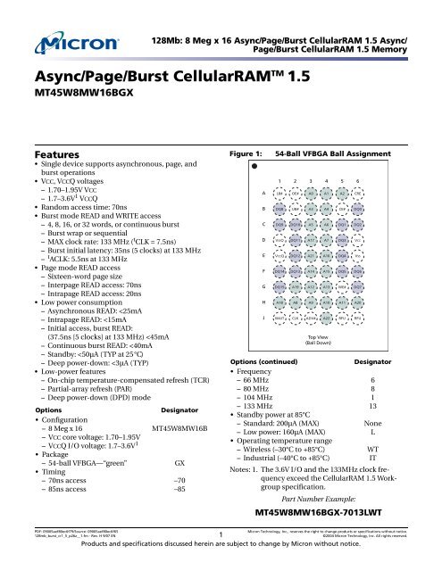
128Mb: Async/Page/Burst CellularRAMtm 1.5 - Micron
128Mb: Async/Page/Burst CellularRAMtm 1.5 - Micron
128Mb: Async/Page/Burst CellularRAMtm 1.5 - Micron

You also want an ePaper? Increase the reach of your titles
YUMPU automatically turns print PDFs into web optimized ePapers that Google loves.
<strong>128Mb</strong>: 8 Meg x 16 <strong>Async</strong>/<strong>Page</strong>/<strong>Burst</strong> CellularRAM <strong>1.5</strong> <strong>Async</strong>/<br />
<strong>Page</strong>/<strong>Burst</strong> CellularRAM <strong>1.5</strong> Memory<br />
<strong>Async</strong>/<strong>Page</strong>/<strong>Burst</strong> CellularRAM TM <strong>1.5</strong><br />
MT45W8MW16BGX<br />
Features<br />
• Single device supports asynchronous, page, and<br />
burst operations<br />
VCC, VCCQ voltages<br />
– 1.70–1.95V VCC<br />
– 1.7–3.6V 1 VCCQ<br />
Random access time: 70ns<br />
<strong>Burst</strong> mode READ and WRITE access<br />
– 4, 8, 16, or 32 words, or continuous burst<br />
– <strong>Burst</strong> wrap or sequential<br />
– MAX clock rate: 133 MHz ( t CLK = 7.5ns)<br />
– <strong>Burst</strong> initial latency: 35ns (5 clocks) at 133 MHz<br />
– t ACLK: 5.5ns at 133 MHz<br />
<strong>Page</strong> mode READ access<br />
– Sixteen-word page size<br />
– Interpage READ access: 70ns<br />
– Intrapage READ access: 20ns<br />
Low power consumption<br />
– <strong>Async</strong>hronous READ:
Table of Contents<br />
<strong>128Mb</strong>: 8 Meg x 16 <strong>Async</strong>/<strong>Page</strong>/<strong>Burst</strong> CellularRAM <strong>1.5</strong><br />
Table of Contents<br />
Features. . . . . . . . . . . . . . . . . . . . . . . . . . . . . . . . . . . . . . . . . . . . . . . . . . . . . . . . . . . . . . . . . . . . . . . . . . . . . . . . . . . . . . . . . . . . . .1<br />
General Description . . . . . . . . . . . . . . . . . . . . . . . . . . . . . . . . . . . . . . . . . . . . . . . . . . . . . . . . . . . . . . . . . . . . . . . . . . . . . . . . . . .5<br />
Part-Numbering Information. . . . . . . . . . . . . . . . . . . . . . . . . . . . . . . . . . . . . . . . . . . . . . . . . . . . . . . . . . . . . . . . . . . . . . . . . . .9<br />
Functional Description . . . . . . . . . . . . . . . . . . . . . . . . . . . . . . . . . . . . . . . . . . . . . . . . . . . . . . . . . . . . . . . . . . . . . . . . . . . . . . .10<br />
Power-Up Initialization . . . . . . . . . . . . . . . . . . . . . . . . . . . . . . . . . . . . . . . . . . . . . . . . . . . . . . . . . . . . . . . . . . . . . . . . . . . .10<br />
Bus Operating Modes . . . . . . . . . . . . . . . . . . . . . . . . . . . . . . . . . . . . . . . . . . . . . . . . . . . . . . . . . . . . . . . . . . . . . . . . . . . . . . . . .10<br />
<strong>Async</strong>hronous Mode . . . . . . . . . . . . . . . . . . . . . . . . . . . . . . . . . . . . . . . . . . . . . . . . . . . . . . . . . . . . . . . . . . . . . . . . . . . . . . .10<br />
<strong>Page</strong> Mode READ Operation . . . . . . . . . . . . . . . . . . . . . . . . . . . . . . . . . . . . . . . . . . . . . . . . . . . . . . . . . . . . . . . . . . . . . . . .12<br />
<strong>Burst</strong> Mode Operation. . . . . . . . . . . . . . . . . . . . . . . . . . . . . . . . . . . . . . . . . . . . . . . . . . . . . . . . . . . . . . . . . . . . . . . . . . . . . .13<br />
Mixed-Mode Operation . . . . . . . . . . . . . . . . . . . . . . . . . . . . . . . . . . . . . . . . . . . . . . . . . . . . . . . . . . . . . . . . . . . . . . . . . . . .15<br />
WAIT Operation . . . . . . . . . . . . . . . . . . . . . . . . . . . . . . . . . . . . . . . . . . . . . . . . . . . . . . . . . . . . . . . . . . . . . . . . . . . . . . . . . . .15<br />
LB#/UB# Operation . . . . . . . . . . . . . . . . . . . . . . . . . . . . . . . . . . . . . . . . . . . . . . . . . . . . . . . . . . . . . . . . . . . . . . . . . . . . . . . .16<br />
Low-Power Operation . . . . . . . . . . . . . . . . . . . . . . . . . . . . . . . . . . . . . . . . . . . . . . . . . . . . . . . . . . . . . . . . . . . . . . . . . . . . . . . .17<br />
Standby Mode . . . . . . . . . . . . . . . . . . . . . . . . . . . . . . . . . . . . . . . . . . . . . . . . . . . . . . . . . . . . . . . . . . . . . . . . . . . . . . . . . . . . .17<br />
Temperature-Compensated Refresh (TCR) . . . . . . . . . . . . . . . . . . . . . . . . . . . . . . . . . . . . . . . . . . . . . . . . . . . . . . . . . . .17<br />
Partial-Array Refresh (PAR) . . . . . . . . . . . . . . . . . . . . . . . . . . . . . . . . . . . . . . . . . . . . . . . . . . . . . . . . . . . . . . . . . . . . . . . . .17<br />
Deep Power-Down Mode (DPD). . . . . . . . . . . . . . . . . . . . . . . . . . . . . . . . . . . . . . . . . . . . . . . . . . . . . . . . . . . . . . . . . . . . .17<br />
Registers . . . . . . . . . . . . . . . . . . . . . . . . . . . . . . . . . . . . . . . . . . . . . . . . . . . . . . . . . . . . . . . . . . . . . . . . . . . . . . . . . . . . . . . . . . . .17<br />
Access Using CRE . . . . . . . . . . . . . . . . . . . . . . . . . . . . . . . . . . . . . . . . . . . . . . . . . . . . . . . . . . . . . . . . . . . . . . . . . . . . . . . . . .18<br />
Software Access. . . . . . . . . . . . . . . . . . . . . . . . . . . . . . . . . . . . . . . . . . . . . . . . . . . . . . . . . . . . . . . . . . . . . . . . . . . . . . . . . . . .22<br />
Bus Configuration Register (BCR). . . . . . . . . . . . . . . . . . . . . . . . . . . . . . . . . . . . . . . . . . . . . . . . . . . . . . . . . . . . . . . . . . . .24<br />
<strong>Burst</strong> Length (BCR[2:0]) Default = Continuous <strong>Burst</strong> . . . . . . . . . . . . . . . . . . . . . . . . . . . . . . . . . . . . . . . . . . . . . . . .25<br />
<strong>Burst</strong> Wrap (BCR[3]) Default = No Wrap . . . . . . . . . . . . . . . . . . . . . . . . . . . . . . . . . . . . . . . . . . . . . . . . . . . . . . . . . . .25<br />
Drive Strength (BCR[5:4]) Default = Outputs Use Half-Drive Strength . . . . . . . . . . . . . . . . . . . . . . . . . . . . . . . . .26<br />
WAIT Configuration (BCR[8]) Default = WAIT Transitions One Clock Before Data Valid/Invalid . . . . . . . . .27<br />
WAIT Polarity (BCR[10]) Default = WAIT Active HIGH . . . . . . . . . . . . . . . . . . . . . . . . . . . . . . . . . . . . . . . . . . . . . . .27<br />
Latency Counter (BCR[13:11]) Default = Three Clock Latency . . . . . . . . . . . . . . . . . . . . . . . . . . . . . . . . . . . . . . . .28<br />
Initial Access Latency (BCR[14]) Default = Variable . . . . . . . . . . . . . . . . . . . . . . . . . . . . . . . . . . . . . . . . . . . . . . . . .28<br />
Operating Mode (BCR[15]) Default = <strong>Async</strong>hronous Operation. . . . . . . . . . . . . . . . . . . . . . . . . . . . . . . . . . . . . . .30<br />
Refresh Configuration Register (RCR) . . . . . . . . . . . . . . . . . . . . . . . . . . . . . . . . . . . . . . . . . . . . . . . . . . . . . . . . . . . . . . . .31<br />
PAR (RCR[2:0]) Default = Full Array Refresh . . . . . . . . . . . . . . . . . . . . . . . . . . . . . . . . . . . . . . . . . . . . . . . . . . . . . . . .31<br />
DPD (RCR[4]) Default = DPD Disabled. . . . . . . . . . . . . . . . . . . . . . . . . . . . . . . . . . . . . . . . . . . . . . . . . . . . . . . . . . . . .32<br />
<strong>Page</strong> Mode Operation (RCR[7]) Default = Disabled. . . . . . . . . . . . . . . . . . . . . . . . . . . . . . . . . . . . . . . . . . . . . . . . . .32<br />
Device Identification Register (DIDR) . . . . . . . . . . . . . . . . . . . . . . . . . . . . . . . . . . . . . . . . . . . . . . . . . . . . . . . . . . . . . . . .32<br />
Electrical Specifications. . . . . . . . . . . . . . . . . . . . . . . . . . . . . . . . . . . . . . . . . . . . . . . . . . . . . . . . . . . . . . . . . . . . . . . . . . . . . . .33<br />
Timing Requirements. . . . . . . . . . . . . . . . . . . . . . . . . . . . . . . . . . . . . . . . . . . . . . . . . . . . . . . . . . . . . . . . . . . . . . . . . . . . . . . . .37<br />
Timing Diagrams. . . . . . . . . . . . . . . . . . . . . . . . . . . . . . . . . . . . . . . . . . . . . . . . . . . . . . . . . . . . . . . . . . . . . . . . . . . . . . . . . . . . .41<br />
Package Information . . . . . . . . . . . . . . . . . . . . . . . . . . . . . . . . . . . . . . . . . . . . . . . . . . . . . . . . . . . . . . . . . . . . . . . . . . . . . . . . .68<br />
PDF: 09005aef80ec6f79/Source: 09005aef80ec6f65 <strong>Micron</strong> Technology, Inc., reserves the right to change products or specifications without notice.<br />
128mb_burst_cr1_5_p26zTOC.fm - Rev. H 9/07 EN 2 ©2004 <strong>Micron</strong> Technology, Inc. All rights reserved.
List of Figures<br />
<strong>128Mb</strong>: 8 Meg x 16 <strong>Async</strong>/<strong>Page</strong>/<strong>Burst</strong> CellularRAM <strong>1.5</strong><br />
List of Figures<br />
Figure 1: 54-Ball VFBGA Ball Assignment . . . . . . . . . . . . . . . . . . . . . . . . . . . . . . . . . . . . . . . . . . . . . . . . . . . . . . . . . . . .1<br />
Figure 2: Functional Block Diagram – 8 Meg x 16 . . . . . . . . . . . . . . . . . . . . . . . . . . . . . . . . . . . . . . . . . . . . . . . . . . . . .6<br />
Figure 3: Part Number Chart . . . . . . . . . . . . . . . . . . . . . . . . . . . . . . . . . . . . . . . . . . . . . . . . . . . . . . . . . . . . . . . . . . . . . . .9<br />
Figure 4: Power-Up Initialization Timing . . . . . . . . . . . . . . . . . . . . . . . . . . . . . . . . . . . . . . . . . . . . . . . . . . . . . . . . . . .10<br />
Figure 5: READ Operation (ADV# LOW) . . . . . . . . . . . . . . . . . . . . . . . . . . . . . . . . . . . . . . . . . . . . . . . . . . . . . . . . . . . .11<br />
Figure 6: WRITE Operation (ADV# LOW) . . . . . . . . . . . . . . . . . . . . . . . . . . . . . . . . . . . . . . . . . . . . . . . . . . . . . . . . . . .11<br />
Figure 7: <strong>Page</strong> Mode READ Operation (ADV# LOW) . . . . . . . . . . . . . . . . . . . . . . . . . . . . . . . . . . . . . . . . . . . . . . . . . .12<br />
Figure 8: <strong>Burst</strong> Mode READ (4-word burst) . . . . . . . . . . . . . . . . . . . . . . . . . . . . . . . . . . . . . . . . . . . . . . . . . . . . . . . . .14<br />
Figure 9: <strong>Burst</strong> Mode WRITE (4-word burst) . . . . . . . . . . . . . . . . . . . . . . . . . . . . . . . . . . . . . . . . . . . . . . . . . . . . . . . .14<br />
Figure 10: Wired-OR WAIT Configuration . . . . . . . . . . . . . . . . . . . . . . . . . . . . . . . . . . . . . . . . . . . . . . . . . . . . . . . . . . . .15<br />
Figure 11: Refresh Collision During Variable-Latency READ Operation . . . . . . . . . . . . . . . . . . . . . . . . . . . . . . . . .16<br />
Figure 12: Configuration Register WRITE, <strong>Async</strong>hronous Mode, Followed by READ ARRAY Operation . . . . .18<br />
Figure 13: Configuration Register WRITE, Synchronous Mode Followed by READ ARRAY Operation . . . . . . .19<br />
Figure 14: Register READ, <strong>Async</strong>hronous Mode Followed by READ ARRAY Operation . . . . . . . . . . . . . . . . . . . .20<br />
Figure 15: Register READ, Synchronous Mode Followed by READ ARRAY Operation . . . . . . . . . . . . . . . . . . . . .21<br />
Figure 16: Load Configuration Register . . . . . . . . . . . . . . . . . . . . . . . . . . . . . . . . . . . . . . . . . . . . . . . . . . . . . . . . . . . . . .22<br />
Figure 17: Read Configuration Register . . . . . . . . . . . . . . . . . . . . . . . . . . . . . . . . . . . . . . . . . . . . . . . . . . . . . . . . . . . . . .23<br />
Figure 18: Bus Configuration Register Definition . . . . . . . . . . . . . . . . . . . . . . . . . . . . . . . . . . . . . . . . . . . . . . . . . . . . .24<br />
Figure 19: WAIT Configuration (BCR[8] = 0) . . . . . . . . . . . . . . . . . . . . . . . . . . . . . . . . . . . . . . . . . . . . . . . . . . . . . . . . . .27<br />
Figure 20: WAIT Configuration (BCR[8] = 1) . . . . . . . . . . . . . . . . . . . . . . . . . . . . . . . . . . . . . . . . . . . . . . . . . . . . . . . . . .27<br />
Figure 22: Latency Counter (Variable Initial Latency, No Refresh Collision) . . . . . . . . . . . . . . . . . . . . . . . . . . . . .29<br />
Figure 24: Refresh Configuration Register Mapping . . . . . . . . . . . . . . . . . . . . . . . . . . . . . . . . . . . . . . . . . . . . . . . . . . .31<br />
Figure 25: Typical Refresh Current vs. Temperature (ITCR) . . . . . . . . . . . . . . . . . . . . . . . . . . . . . . . . . . . . . . . . . . . . .35<br />
Figure 26: AC Input/Output Reference Waveform . . . . . . . . . . . . . . . . . . . . . . . . . . . . . . . . . . . . . . . . . . . . . . . . . . . .36<br />
Figure 27: AC Output Load Circuit . . . . . . . . . . . . . . . . . . . . . . . . . . . . . . . . . . . . . . . . . . . . . . . . . . . . . . . . . . . . . . . . . .36<br />
Figure 28: Initialization Period . . . . . . . . . . . . . . . . . . . . . . . . . . . . . . . . . . . . . . . . . . . . . . . . . . . . . . . . . . . . . . . . . . . . . .41<br />
Figure 29: DPD Entry and Exit Timing Parameters . . . . . . . . . . . . . . . . . . . . . . . . . . . . . . . . . . . . . . . . . . . . . . . . . . . .41<br />
Figure 30: <strong>Async</strong>hronous READ . . . . . . . . . . . . . . . . . . . . . . . . . . . . . . . . . . . . . . . . . . . . . . . . . . . . . . . . . . . . . . . . . . . . .42<br />
Figure 31: <strong>Async</strong>hronous READ Using ADV# . . . . . . . . . . . . . . . . . . . . . . . . . . . . . . . . . . . . . . . . . . . . . . . . . . . . . . . . .43<br />
Figure 32: <strong>Page</strong> Mode READ . . . . . . . . . . . . . . . . . . . . . . . . . . . . . . . . . . . . . . . . . . . . . . . . . . . . . . . . . . . . . . . . . . . . . . . .44<br />
Figure 33: Single-Access <strong>Burst</strong> READ Operation – Variable Latency . . . . . . . . . . . . . . . . . . . . . . . . . . . . . . . . . . . . .45<br />
Figure 34: 4-Word <strong>Burst</strong> READ Operation – Variable Latency . . . . . . . . . . . . . . . . . . . . . . . . . . . . . . . . . . . . . . . . . .46<br />
Figure 35: Single-Access <strong>Burst</strong> READ Operation – Fixed Latency . . . . . . . . . . . . . . . . . . . . . . . . . . . . . . . . . . . . . . .47<br />
Figure 36: 4-Word <strong>Burst</strong> READ Operation – Fixed Latency . . . . . . . . . . . . . . . . . . . . . . . . . . . . . . . . . . . . . . . . . . . . .48<br />
Figure 37: READ <strong>Burst</strong> Suspend . . . . . . . . . . . . . . . . . . . . . . . . . . . . . . . . . . . . . . . . . . . . . . . . . . . . . . . . . . . . . . . . . . . . .49<br />
Figure 38: <strong>Burst</strong> READ at End of Row (Wrap Off) . . . . . . . . . . . . . . . . . . . . . . . . . . . . . . . . . . . . . . . . . . . . . . . . . . . . . .50<br />
Figure 39: CE#-Controlled <strong>Async</strong>hronous WRITE . . . . . . . . . . . . . . . . . . . . . . . . . . . . . . . . . . . . . . . . . . . . . . . . . . . . .51<br />
Figure 40: LB#/UB#-Controlled <strong>Async</strong>hronous WRITE . . . . . . . . . . . . . . . . . . . . . . . . . . . . . . . . . . . . . . . . . . . . . . . .52<br />
Figure 41: WE#-Controlled <strong>Async</strong>hronous WRITE . . . . . . . . . . . . . . . . . . . . . . . . . . . . . . . . . . . . . . . . . . . . . . . . . . . .53<br />
Figure 42: <strong>Async</strong>hronous WRITE Using ADV# . . . . . . . . . . . . . . . . . . . . . . . . . . . . . . . . . . . . . . . . . . . . . . . . . . . . . . . .54<br />
Figure 43: <strong>Burst</strong> WRITE Operation – Variable Latency Mode . . . . . . . . . . . . . . . . . . . . . . . . . . . . . . . . . . . . . . . . . . .55<br />
Figure 44: <strong>Burst</strong> WRITE Operation – Fixed Latency Mode . . . . . . . . . . . . . . . . . . . . . . . . . . . . . . . . . . . . . . . . . . . . . .56<br />
Figure 45: <strong>Burst</strong> WRITE at End of Row (Wrap Off) . . . . . . . . . . . . . . . . . . . . . . . . . . . . . . . . . . . . . . . . . . . . . . . . . . . . .57<br />
Figure 46: <strong>Burst</strong> WRITE Followed by <strong>Burst</strong> READ . . . . . . . . . . . . . . . . . . . . . . . . . . . . . . . . . . . . . . . . . . . . . . . . . . . . .58<br />
Figure 47: <strong>Burst</strong> READ Interrupted by <strong>Burst</strong> READ or WRITE . . . . . . . . . . . . . . . . . . . . . . . . . . . . . . . . . . . . . . . . . . .59<br />
Figure 48: <strong>Burst</strong> WRITE Interrupted by <strong>Burst</strong> WRITE or READ – Variable Latency Mode . . . . . . . . . . . . . . . . . .60<br />
Figure 49: <strong>Burst</strong> WRITE Interrupted by <strong>Burst</strong> WRITE or READ – Fixed Latency Mode . . . . . . . . . . . . . . . . . . . . .61<br />
Figure 50: <strong>Async</strong>hronous WRITE Followed by <strong>Burst</strong> READ . . . . . . . . . . . . . . . . . . . . . . . . . . . . . . . . . . . . . . . . . . . . .62<br />
Figure 51: <strong>Async</strong>hronous WRITE (ADV# LOW) Followed by <strong>Burst</strong> READ . . . . . . . . . . . . . . . . . . . . . . . . . . . . . . . . .63<br />
Figure 52: <strong>Burst</strong> READ Followed by <strong>Async</strong>hronous WRITE (WE#-Controlled) . . . . . . . . . . . . . . . . . . . . . . . . . . . .64<br />
Figure 53: <strong>Burst</strong> READ Followed by <strong>Async</strong>hronous WRITE Using ADV# . . . . . . . . . . . . . . . . . . . . . . . . . . . . . . . . .65<br />
Figure 54: <strong>Async</strong>hronous WRITE Followed by <strong>Async</strong>hronous READ – ADV# LOW . . . . . . . . . . . . . . . . . . . . . . . .66<br />
Figure 56: 54-Ball VFBGA . . . . . . . . . . . . . . . . . . . . . . . . . . . . . . . . . . . . . . . . . . . . . . . . . . . . . . . . . . . . . . . . . . . . . . . . . .68<br />
PDF: 09005aef80ec6f79/Source: 09005aef80ec6f65 <strong>Micron</strong> Technology, Inc., reserves the right to change products or specifications without notice.<br />
128mb_burst_cr1_5_p26zLOF.fm - Rev. H 9/07 EN 3 ©2004 <strong>Micron</strong> Technology, Inc. All rights reserved.
List of Tables<br />
<strong>128Mb</strong>: 8 Meg x 16 <strong>Async</strong>/<strong>Page</strong>/<strong>Burst</strong> CellularRAM <strong>1.5</strong><br />
List of Tables<br />
Table 1: VFBGA Ball Descriptions. . . . . . . . . . . . . . . . . . . . . . . . . . . . . . . . . . . . . . . . . . . . . . . . . . . . . . . . . . . . . . . . . . .7<br />
Table 2: Bus Operations . . . . . . . . . . . . . . . . . . . . . . . . . . . . . . . . . . . . . . . . . . . . . . . . . . . . . . . . . . . . . . . . . . . . . . . . . . .8<br />
Table 3: Sequence and <strong>Burst</strong> Length . . . . . . . . . . . . . . . . . . . . . . . . . . . . . . . . . . . . . . . . . . . . . . . . . . . . . . . . . . . . . . .25<br />
Table 4: Drive Strength . . . . . . . . . . . . . . . . . . . . . . . . . . . . . . . . . . . . . . . . . . . . . . . . . . . . . . . . . . . . . . . . . . . . . . . . . . .26<br />
Table 5: Variable Latency Configuration Codes . . . . . . . . . . . . . . . . . . . . . . . . . . . . . . . . . . . . . . . . . . . . . . . . . . . . .28<br />
Table 6: Fixed Latency Configuration Codes . . . . . . . . . . . . . . . . . . . . . . . . . . . . . . . . . . . . . . . . . . . . . . . . . . . . . . . .29<br />
Table 7: <strong>128Mb</strong> Address Patterns for PAR (RCR[4] = 1) . . . . . . . . . . . . . . . . . . . . . . . . . . . . . . . . . . . . . . . . . . . . . . .32<br />
Table 8: Device Identification Register Mapping . . . . . . . . . . . . . . . . . . . . . . . . . . . . . . . . . . . . . . . . . . . . . . . . . . . .32<br />
Table 9: Absolute Maximum Ratings . . . . . . . . . . . . . . . . . . . . . . . . . . . . . . . . . . . . . . . . . . . . . . . . . . . . . . . . . . . . . . .33<br />
Table 10: Electrical Characteristics and Operating Conditions . . . . . . . . . . . . . . . . . . . . . . . . . . . . . . . . . . . . . . . . .34<br />
Table 11: PAR Specifications and Conditions . . . . . . . . . . . . . . . . . . . . . . . . . . . . . . . . . . . . . . . . . . . . . . . . . . . . . . . .35<br />
Table 12: Deep Power-Down Specifications . . . . . . . . . . . . . . . . . . . . . . . . . . . . . . . . . . . . . . . . . . . . . . . . . . . . . . . . .36<br />
Table 13: Capacitance . . . . . . . . . . . . . . . . . . . . . . . . . . . . . . . . . . . . . . . . . . . . . . . . . . . . . . . . . . . . . . . . . . . . . . . . . . . . .36<br />
Table 14: <strong>Async</strong>hronous READ Cycle Timing Requirements . . . . . . . . . . . . . . . . . . . . . . . . . . . . . . . . . . . . . . . . . . .37<br />
Table 15: <strong>Burst</strong> READ Cycle Timing Requirements . . . . . . . . . . . . . . . . . . . . . . . . . . . . . . . . . . . . . . . . . . . . . . . . . . .38<br />
Table 16: <strong>Async</strong>hronous WRITE Cycle Timing Requirements . . . . . . . . . . . . . . . . . . . . . . . . . . . . . . . . . . . . . . . . . .39<br />
Table 17: <strong>Burst</strong> WRITE Cycle Timing Requirements . . . . . . . . . . . . . . . . . . . . . . . . . . . . . . . . . . . . . . . . . . . . . . . . . .40<br />
Table 18: Initialization and DPD Timing Parameters. . . . . . . . . . . . . . . . . . . . . . . . . . . . . . . . . . . . . . . . . . . . . . . . . .41<br />
PDF: 09005aef80ec6f79/Source: 09005aef80ec6f65 <strong>Micron</strong> Technology, Inc., reserves the right to change products or specifications without notice.<br />
128mb_burst_cr1_5_p26zLOT.fm - Rev. H 9/07 EN 4 ©2004 <strong>Micron</strong> Technology, Inc. All rights reserved.
General Description<br />
<strong>128Mb</strong>: 8 Meg x 16 <strong>Async</strong>/<strong>Page</strong>/<strong>Burst</strong> CellularRAM <strong>1.5</strong> <strong>Async</strong>/<br />
<strong>Page</strong>/<strong>Burst</strong> CellularRAM <strong>1.5</strong> Memory<br />
<strong>Micron</strong> ® CellularRAM is a high-speed, CMOS pseudo-static random access memory<br />
developed for low-power, portable applications. The MT45W8MW16BGX device has a<br />
<strong>128Mb</strong> DRAM core, organized as 8 Meg x 16 bits. These devices include an industrystandard<br />
burst mode Flash interface that dramatically increases read/write bandwidth<br />
compared with other low-power SRAM or pseudo-SRAM offerings.<br />
To operate seamlessly on a burst Flash bus, CellularRAM products incorporate a transparent<br />
self refresh mechanism. The hidden refresh requires no additional support from<br />
the system memory controller and has no significant impact on device read/write<br />
performance.<br />
Two user-accessible control registers define device operation. The bus configuration<br />
register (BCR) defines how the CellularRAM device interacts with the system memory<br />
bus and is nearly identical to its counterpart on burst mode Flash devices. The refresh<br />
configuration register (RCR) is used to control how refresh is performed on the DRAM<br />
array. These registers are automatically loaded with default settings during power-up<br />
and can be updated anytime during normal operation.<br />
Special attention has been focused on standby current consumption during self refresh.<br />
CellularRAM products include three mechanisms to minimize standby current. Partialarray<br />
refresh (PAR) enables the system to limit refresh to only that part of the DRAM<br />
array that contains essential data. Temperature-compensated refresh (TCR) uses an onchip<br />
sensor to adjust the refresh rate to match the device temperature—the refresh rate<br />
decreases at lower temperatures to minimize current consumption during standby.<br />
Deep power-down (DPD) enables the system to halt the refresh operation altogether<br />
when no vital information is stored in the device. The system-configurable refresh<br />
mechanisms are accessed through the RCR.<br />
This CellularRAM device is compliant with the industry-standard CellularRAM <strong>1.5</strong><br />
feature set established by the CellularRAM Workgroup. It includes support for both variable<br />
and fixed latency, with three output-device drive-strength settings, additional wrap<br />
options, and a device ID register (DIDR).<br />
PDF: 09005aef80ec6f79/Source: 09005aef80ec6f65 <strong>Micron</strong> Technology, Inc., reserves the right to change products or specifications without notice.<br />
128mb_burst_cr1_5_p26z__2.fm - Rev. H 9/07 EN 5 ©2004 <strong>Micron</strong> Technology, Inc. All rights reserved.
Figure 2: Functional Block Diagram – 8 Meg x 16<br />
CE#<br />
WE#<br />
OE#<br />
CLK<br />
ADV#<br />
CRE<br />
WAIT<br />
LB#<br />
UB#<br />
A[22:0]<br />
Control<br />
Logic<br />
<strong>128Mb</strong>: 8 Meg x 16 <strong>Async</strong>/<strong>Page</strong>/<strong>Burst</strong> CellularRAM <strong>1.5</strong> <strong>Async</strong>/<br />
<strong>Page</strong>/<strong>Burst</strong> CellularRAM <strong>1.5</strong> Memory<br />
Address Decode<br />
Logic<br />
Refresh Configuration<br />
Register (RCR)<br />
Device ID Register<br />
(DIDR)<br />
Bus Configuration<br />
Register (BCR)<br />
8,192K x 16<br />
DRAM<br />
Memory<br />
Array<br />
Input/<br />
Output<br />
MUX<br />
and<br />
Buffers<br />
DQ[7:0]<br />
DQ[15:8]<br />
Notes: 1. Functional block diagrams illustrate simplified device operation. See ball descriptions<br />
(Table 1 on page 7), bus operations table (Table 2 on page 8), and timing diagrams for<br />
detailed information.<br />
PDF: 09005aef80ec6f79/Source: 09005aef80ec6f65 <strong>Micron</strong> Technology, Inc., reserves the right to change products or specifications without notice.<br />
128mb_burst_cr1_5_p26z__2.fm - Rev. H 9/07 EN 6 ©2004 <strong>Micron</strong> Technology, Inc. All rights reserved.
Table 1: VFBGA Ball Descriptions<br />
Note 1<br />
<strong>128Mb</strong>: 8 Meg x 16 <strong>Async</strong>/<strong>Page</strong>/<strong>Burst</strong> CellularRAM <strong>1.5</strong> <strong>Async</strong>/<br />
<strong>Page</strong>/<strong>Burst</strong> CellularRAM <strong>1.5</strong> Memory<br />
VFBGA Assignment Symbol Type Description<br />
J4, E3, H6, G2, H1,<br />
D3, E4, F4, F3, G4, G3,<br />
H5, H4, H3, H2, D4,<br />
C4, C3, B4, B3, A5,<br />
A4, A3<br />
A[22:0] Input Address inputs: Inputs for addresses during READ and WRITE operations.<br />
Addresses are internally latched during READ and WRITE cycles. The address<br />
lines are also used to define the value to be loaded into the BCR or the RCR.<br />
J2 CLK Input Clock: Synchronizes the memory to the system operating frequency during<br />
synchronous operations. When configured for synchronous operation, the<br />
address is latched on the first rising CLK edge when ADV# is active. CLK is<br />
static LOW during asynchronous access READ and WRITE operations and<br />
during PAGE READ ACCESS operations.<br />
J3 ADV# Input Address valid: Indicates that a valid address is present on the address inputs.<br />
Addresses can be latched on the rising edge of ADV# during asynchronous<br />
READ and WRITE operations. ADV# can be held LOW during asynchronous<br />
READ and WRITE operations.<br />
A6 CRE Input Control register enable: When CRE is HIGH, WRITE operations load the RCR<br />
or BCR, and READ operations access the RCR, BCR, or DIDR.<br />
B5 CE# Input Chip enable: Activates the device when LOW. When CE# is HIGH, the device<br />
is disabled and goes into standby or deep power-down mode.<br />
A2 OE# Input Output enable: Enables the output buffers when LOW. When OE# is HIGH,<br />
the output buffers are disabled.<br />
G5 WE# Input Write enable: Determines if a given cycle is a WRITE cycle. If WE# is LOW,<br />
the cycle is a WRITE to either a configuration register or to the memory<br />
array.<br />
A1 LB# Input Lower byte enable. DQ[7:0]<br />
B2 UB# Input Upper byte enable. DQ[15:8]<br />
G1, F1, F2, E2, D2, C2,<br />
C1, B1, G6, F6, F5, E5,<br />
D5, C6, C5, B6<br />
DQ[15:0] Input/<br />
Output<br />
Data inputs/outputs.<br />
J1 WAIT Output Wait: Provides data-valid feedback during burst READ and WRITE<br />
operations. The signal is gated by CE#. WAIT is used to arbitrate collisions<br />
between refresh and READ/WRITE operations. WAIT is also asserted at the<br />
end of a row unless wrapping within the burst length. WAIT is asserted and<br />
should be ignored during asynchronous and page mode operations. WAIT is<br />
High-Z when CE# is HIGH.<br />
J5, J6 RFU — Reserved for future use.<br />
D6 VCC Supply Device power supply: (1.7–1.95V) Power supply for device core operation.<br />
E1 VCCQ Supply I/O power supply: (1.7–3.6V) Power supply for input/output buffers.<br />
E6 VSS Supply VSS must be connected to ground.<br />
D1 VSSQ Supply VSSQ must be connected to ground.<br />
Notes: 1. The CLK and ADV# inputs can be tied to VSS if the device is always operating in asynchronous<br />
or page mode. WAIT will be asserted but should be ignored during asynchronous and<br />
page mode operations.<br />
PDF: 09005aef80ec6f79/Source: 09005aef80ec6f65 <strong>Micron</strong> Technology, Inc., reserves the right to change products or specifications without notice.<br />
128mb_burst_cr1_5_p26z__2.fm - Rev. H 9/07 EN 7 ©2004 <strong>Micron</strong> Technology, Inc. All rights reserved.
Table 2: Bus Operations<br />
<strong>128Mb</strong>: 8 Meg x 16 <strong>Async</strong>/<strong>Page</strong>/<strong>Burst</strong> CellularRAM <strong>1.5</strong> <strong>Async</strong>/<br />
<strong>Page</strong>/<strong>Burst</strong> CellularRAM <strong>1.5</strong> Memory<br />
<strong>Async</strong>hronous Mode<br />
BCR[15] = 1 Power CLK 1 ADV# CE# OE# WE# CRE<br />
LB#/<br />
UB# WAIT 2 DQ[15:0] 3 Notes<br />
Read Active L L L L H L L Low-Z Data-out 4<br />
Write Active L L L X L L L Low-Z Data-in 4<br />
Standby Standby L X H X X L X High-Z High-Z 5, 6<br />
No operation Idle L X L X X L X Low-Z X 4, 6<br />
Configuration register<br />
write<br />
Active L L L H L H X Low-Z High-Z<br />
Configuration register Active L L L L H H L Low-Z Config.<br />
read<br />
reg. out<br />
DPD Deep<br />
power-down<br />
L X H X X X X High-Z High-Z 7<br />
<strong>Burst</strong> Mode<br />
BCR[15] = 0 Power CLK1 ADV# CE# OE# WE# CRE<br />
LB#/<br />
UB# WAIT2 DQ[15:0] 3 Notes<br />
<strong>Async</strong> read Active L L L L H L L Low-Z Data-out 4<br />
<strong>Async</strong> write Active L L L X L L L Low-Z Data-in 4<br />
Standby Standby L X H X X L X High-Z High-Z 5, 6<br />
No operation Idle L X L X X L X Low-Z X 4, 6<br />
Initial burst read Active L L X H L L Low-Z X 4, 8<br />
Initial burst write Active L L H L L X Low-Z X 4, 8<br />
<strong>Burst</strong> continue Active H L X X X L Low-Z Data-in or<br />
Data-out<br />
<strong>Burst</strong> suspend Active X X L H X X X Low-Z High-Z 4, 8<br />
Configuration register<br />
write<br />
Active L L H L H X Low-Z High-Z 8, 9<br />
Configuration register<br />
read<br />
DPD Deep<br />
power-down<br />
Active L L L H H L Low-Z Config.<br />
reg. out<br />
L X H X X X X High-Z High-Z 7<br />
Notes: 1. CLK must be LOW during async read and async write modes; and to achieve standby power<br />
during standby and DPD modes. CLK must be static (HIGH or LOW) during burst suspend.<br />
2. The WAIT polarity is configured through the bus configuration register (BCR[10]).<br />
3. When LB# and UB# are in select mode (LOW), DQ[15:0] are affected. When only LB# is in<br />
select mode, DQ[7:0] are affected. When only UB# is in the select mode, DQ[15:8] are<br />
affected.<br />
4. The device will consume active power in this mode whenever addresses are changed.<br />
5. When the device is in standby mode, address inputs and data inputs/outputs are internally<br />
isolated from any external influence.<br />
6. VIN = VCCQ or 0V; all device balls must be static (unswitched) in order to achieve standby current.<br />
7. DPD is initiated when CE# transitions from LOW to HIGH after writing RCR[4] to 0. DPD is<br />
maintained until CE# transitions from HIGH to LOW.<br />
8. <strong>Burst</strong> mode operation is initialized through the bus configuration register (BCR[15]).<br />
9. Initial cycle. Following cycles are the same as BURST CONTINUE. CE# must stay LOW for the<br />
equivalent of a single-word burst (as indicated by WAIT).<br />
PDF: 09005aef80ec6f79/Source: 09005aef80ec6f65 <strong>Micron</strong> Technology, Inc., reserves the right to change products or specifications without notice.<br />
128mb_burst_cr1_5_p26z__2.fm - Rev. H 9/07 EN 8 ©2004 <strong>Micron</strong> Technology, Inc. All rights reserved.<br />
4, 8<br />
8, 9
Part-Numbering Information<br />
Figure 3: Part Number Chart<br />
<strong>128Mb</strong>: 8 Meg x 16 <strong>Async</strong>/<strong>Page</strong>/<strong>Burst</strong> CellularRAM <strong>1.5</strong> <strong>Async</strong>/<br />
<strong>Page</strong>/<strong>Burst</strong> CellularRAM <strong>1.5</strong> Memory<br />
<strong>Micron</strong> CellularRAM devices are available in several different configurations and<br />
densities. (See Figure 3.)<br />
<strong>Micron</strong> Technology<br />
Product Family<br />
45 = PSRAM/CellularRAM memory<br />
Operating Core Voltage<br />
W = 1.70–1.95V<br />
Address Locations<br />
M = Megabits<br />
Operating Voltage<br />
W = 1.7–3.6V3 Bus Configuration<br />
16 = x16<br />
READ/WRITE Operation Mode<br />
B = <strong>Async</strong>hronous/<strong>Page</strong>/<strong>Burst</strong><br />
MT 45 W 8M W 16 B GX -70 8 WT ES<br />
Package Codes<br />
GX = 54-ball “green” VFBGA (6 x 9 grid, 0.75mm pitch, 8.0mm x 10.0mm x 1.0mm)<br />
Production Status<br />
Blank = Production<br />
ES = Engineering sample<br />
MS = Mechanical sample<br />
Operating Temperature<br />
WT = –30°C to +85°C<br />
IT = –40°C to +85°C<br />
Standby Power Options<br />
Blank = Standard<br />
L = Low power<br />
Frequency<br />
6 = 66 MHz<br />
8 = 80 MHz<br />
1 = 104 MHz<br />
13 = 133 MHz<br />
Access/Cycle Time<br />
70 = 70ns<br />
85 = 85ns<br />
Notes: 1. Valid part number combinations: After building the part number from the part numbering<br />
chart above, please go to the <strong>Micron</strong> Parametric Part Search Web site at<br />
http://www.micron.com/support/designsupport/tools/fbga/decoder to verify that the part<br />
number is offered and valid. If the device required is not on this list, please contact the<br />
factory.<br />
2. Device marking: Due to the size of the package, the <strong>Micron</strong> standard part number is not<br />
printed on the top of the device. Instead, an abbreviated device mark consisting of a fivedigit<br />
alphanumeric code is used. The abbreviated device marks are cross-referenced to the<br />
<strong>Micron</strong> part numbers at http://www.micron.com/support/designsupport/tools/fbga/decoder.<br />
To view the location of the abbreviated mark on the device, please refer to customer service<br />
note CSN-11, “Product Mark/Label,” at http://www.micron.com/csn.<br />
3. The 3.6V I/O exceeds the CellularRAM <strong>1.5</strong> Workgroup specification of 1.95V.<br />
PDF: 09005aef80ec6f79/Source: 09005aef80ec6f65 <strong>Micron</strong> Technology, Inc., reserves the right to change products or specifications without notice.<br />
128mb_burst_cr1_5_p26z__2.fm - Rev. H 9/07 EN 9 ©2004 <strong>Micron</strong> Technology, Inc. All rights reserved.
Functional Description<br />
Power-Up Initialization<br />
Figure 4: Power-Up Initialization Timing<br />
Bus Operating Modes<br />
<strong>Async</strong>hronous Mode<br />
<strong>128Mb</strong>: 8 Meg x 16 <strong>Async</strong>/<strong>Page</strong>/<strong>Burst</strong> CellularRAM <strong>1.5</strong> <strong>Async</strong>/<br />
<strong>Page</strong>/<strong>Burst</strong> CellularRAM <strong>1.5</strong> Memory<br />
In general, the MT45W8MW16BGX device is a high-density alternative to SRAM and<br />
pseudo-SRAM products, popular in low-power, portable applications.<br />
The MT45W8MW16BGX contains a 134,217,728-bit DRAM core, organized as 8,388,608<br />
addresses by 16 bits. The device implements the same high-speed bus interface found<br />
on burst mode Flash products.<br />
The CellularRAM bus interface supports both asynchronous and burst mode transfers.<br />
<strong>Page</strong> mode accesses are also included as a bandwidth-enhancing extension to the asynchronous<br />
read protocol.<br />
CellularRAM products include an on-chip voltage sensor used to launch the power-up<br />
initialization process. Initialization will configure the BCR and the RCR with their default<br />
settings. (See Figure 18 on page 24 and Figure 24 on page 31.) VCC and VCCQ must be<br />
applied simultaneously. When they reach a stable level at or above 1.7V, the device will<br />
require 150µs to complete its self-initialization process. During the initialization period,<br />
CE# should remain HIGH. When initialization is complete, the device is ready for<br />
normal operation.<br />
VCC<br />
VCCQ<br />
VCC = 1.7V<br />
tPU > 150µs<br />
Device initialization<br />
Device ready for<br />
normal operation<br />
The MT45W8MW16BGX CellularRAM product incorporates a burst mode interface<br />
found on Flash products targeting low-power, wireless applications. This bus interface<br />
supports asynchronous, page mode, and burst mode read and write transfers. The<br />
specific interface supported is defined by the value loaded into the BCR. <strong>Page</strong> mode is<br />
controlled by the refresh configuration register (RCR[7]).<br />
CellularRAM <strong>1.5</strong> products power up in the asynchronous operating mode. This mode<br />
uses the industry-standard SRAM control bus (CE#, OE#, WE#, LB#/UB#). READ operations<br />
(Figure 5 on page 11) are initiated by bringing CE#, OE#, and LB#/UB# LOW while<br />
keeping WE# HIGH. Valid data will be driven out of the I/Os after the specified access<br />
time has elapsed. WRITE operations (see Figure 6 on page 11) occur when CE#, WE#,<br />
and LB#/UB# are driven LOW. During asynchronous WRITE operations, the OE# level is<br />
a “Don't Care,” and WE# will override OE#. The data to be written is latched on the rising<br />
edge of CE#, WE#, or LB#/UB# (whichever occurs first). <strong>Async</strong>hronous operations (page<br />
mode disabled) can either use the ADV# input to latch the address, or ADV# can be<br />
driven LOW during the entire READ/WRITE operation.<br />
During asynchronous operation, the CLK input must be held static LOW. WAIT will be<br />
driven while the device is enabled and its state should be ignored. WE# LOW time must<br />
be limited to t CEM.<br />
PDF: 09005aef80ec6f79/Source: 09005aef80ec6f65 <strong>Micron</strong> Technology, Inc., reserves the right to change products or specifications without notice.<br />
128mb_burst_cr1_5_p26z__2.fm - Rev. H 9/07 EN 10 ©2004 <strong>Micron</strong> Technology, Inc. All rights reserved.
Figure 5: READ Operation (ADV# LOW)<br />
CE#<br />
OE#<br />
WE#<br />
ADDRESS<br />
DATA<br />
LB#/UB#<br />
<strong>128Mb</strong>: 8 Meg x 16 <strong>Async</strong>/<strong>Page</strong>/<strong>Burst</strong> CellularRAM <strong>1.5</strong> <strong>Async</strong>/<br />
<strong>Page</strong>/<strong>Burst</strong> CellularRAM <strong>1.5</strong> Memory<br />
Notes: 1. ADV# must remain LOW for page mode operation.<br />
Figure 6: WRITE Operation (ADV# LOW)<br />
CE#<br />
OE#<br />
WE#<br />
ADDRESS<br />
DATA<br />
LB#/UB#<br />
Address Valid<br />
Data Valid<br />
t RC = READ cycle time<br />
< tCEM<br />
Address Valid<br />
Data Valid<br />
tWC = WRITE cycle time<br />
Don’t Care<br />
Don’t Care<br />
PDF: 09005aef80ec6f79/Source: 09005aef80ec6f65 <strong>Micron</strong> Technology, Inc., reserves the right to change products or specifications without notice.<br />
128mb_burst_cr1_5_p26z__2.fm - Rev. H 9/07 EN 11 ©2004 <strong>Micron</strong> Technology, Inc. All rights reserved.
<strong>Page</strong> Mode READ Operation<br />
<strong>128Mb</strong>: 8 Meg x 16 <strong>Async</strong>/<strong>Page</strong>/<strong>Burst</strong> CellularRAM <strong>1.5</strong> <strong>Async</strong>/<br />
<strong>Page</strong>/<strong>Burst</strong> CellularRAM <strong>1.5</strong> Memory<br />
<strong>Page</strong> mode is a performance-enhancing extension to the legacy asynchronous READ<br />
operation. In page-mode-capable products, an initial asynchronous read access is<br />
performed, then adjacent addresses can be read quickly by simply changing the loworder<br />
address. Addresses A[3:0] are used to determine the members of the 16-address<br />
CellularRAM page. Any change in addresses A[4] or higher will initiate a new tAA access<br />
time. Figure 7 shows the timing for a page mode access. <strong>Page</strong> mode takes advantage of<br />
the fact that adjacent addresses can be read in a shorter period of time than random<br />
addresses. WRITE operations do not include comparable page mode functionality.<br />
During asynchronous page mode operation, the CLK input must be held LOW. CE# must<br />
be driven HIGH upon completion of a page mode access. WAIT will be driven while the<br />
device is enabled and its state should be ignored. <strong>Page</strong> mode is enabled by setting<br />
RCR[7] to HIGH. ADV# must be driven LOW during all page mode read accesses.<br />
Due to refresh considerations, CE# must not be LOW longer than tCEM. Figure 7: <strong>Page</strong> Mode READ Operation (ADV# LOW)<br />
CE#<br />
OE#<br />
WE#<br />
ADDRESS Add 0 Add 1 Add 2 Add 3<br />
DATA<br />
LB#/UB#<br />
tAA<br />
D1 D2 D3<br />
Don’t Care<br />
PDF: 09005aef80ec6f79/Source: 09005aef80ec6f65 <strong>Micron</strong> Technology, Inc., reserves the right to change products or specifications without notice.<br />
128mb_burst_cr1_5_p26z__2.fm - Rev. H 9/07 EN 12 ©2004 <strong>Micron</strong> Technology, Inc. All rights reserved.<br />
tAPA<br />
D0<br />
< t CEM<br />
tAPA tAPA
<strong>Burst</strong> Mode Operation<br />
<strong>128Mb</strong>: 8 Meg x 16 <strong>Async</strong>/<strong>Page</strong>/<strong>Burst</strong> CellularRAM <strong>1.5</strong> <strong>Async</strong>/<br />
<strong>Page</strong>/<strong>Burst</strong> CellularRAM <strong>1.5</strong> Memory<br />
<strong>Burst</strong> mode operations enable high-speed synchronous READ and WRITE operations.<br />
<strong>Burst</strong> operations consist of a multi-clock sequence that must be performed in an<br />
ordered fashion. After CE# goes LOW, the address to access is latched on the rising edge<br />
of the next clock that ADV# is LOW. During this first clock rising edge, WE# indicates<br />
whether the operation is going to be a READ (WE# = HIGH, in Figure 8 on page 14) or<br />
WRITE (WE# = LOW, in Figure 9 on page 14).<br />
The size of a burst can be specified in the BCR either as a fixed length or as continuous.<br />
Fixed-length bursts consist of four, eight, sixteen, or thirty-two words. Continuous<br />
bursts have the ability to start at a specified address and burst to the end of the 128-word<br />
row.<br />
The latency count stored in the BCR defines the number of clock cycles that elapse<br />
before the initial data value is transferred between the processor and CellularRAM<br />
device. The initial latency for READ operations can be configured as fixed or variable<br />
(WRITE operations always use fixed latency). Variable latency enables the CellularRAM<br />
to be configured for minimum latency at high clock frequencies, but the controller must<br />
monitor WAIT to detect any conflict with refresh cycles.<br />
Fixed latency outputs the first data word after the worst-case access delay, including<br />
allowance for refresh collisions. The initial latency time and clock speed determine the<br />
latency count setting. Fixed latency is used when the controller cannot monitor WAIT.<br />
Fixed latency also provides improved performance at lower clock frequencies.<br />
The WAIT output asserts when a burst is initiated and de-asserts to indicate when data is<br />
to be transferred into (or out of) the memory. WAIT will again be asserted at the<br />
boundary of the 128-word row unless wrapping within the burst length.<br />
To access other devices on the same bus without the timing penalty of the initial latency<br />
for a new burst, burst mode can be suspended. <strong>Burst</strong>s are suspended by stopping CLK.<br />
CLK can be stopped HIGH or LOW. If another device will use the data bus while the burst<br />
is suspended, OE# should be taken HIGH to disable the CellularRAM outputs; otherwise,<br />
OE# can remain LOW. Note that the WAIT output will continue to be active, and as a<br />
result, no other devices should directly share the WAIT connection to the controller. To<br />
continue the burst sequence, OE# is taken LOW, then CLK is restarted after valid data is<br />
available on the bus.<br />
The CE# LOW time is limited by refresh considerations. CE# must not stay LOW longer<br />
than t CEM. If a burst suspension will cause CE# to remain LOW for longer than t CEM,<br />
CE# should be taken HIGH and the burst restarted with a new CE# LOW/ADV# LOW<br />
cycle.<br />
PDF: 09005aef80ec6f79/Source: 09005aef80ec6f65 <strong>Micron</strong> Technology, Inc., reserves the right to change products or specifications without notice.<br />
128mb_burst_cr1_5_p26z__2.fm - Rev. H 9/07 EN 13 ©2004 <strong>Micron</strong> Technology, Inc. All rights reserved.
Figure 8: <strong>Burst</strong> Mode READ (4-word burst)<br />
CLK<br />
A[22:0]<br />
ADV#<br />
CE#<br />
OE#<br />
WE#<br />
WAIT<br />
DQ[15:0]<br />
LB#/UB#<br />
<strong>128Mb</strong>: 8 Meg x 16 <strong>Async</strong>/<strong>Page</strong>/<strong>Burst</strong> CellularRAM <strong>1.5</strong> <strong>Async</strong>/<br />
<strong>Page</strong>/<strong>Burst</strong> CellularRAM <strong>1.5</strong> Memory<br />
Notes: 1. Non-default BCR settings for burst mode READ (4-word burst): Fixed or variable latency;<br />
latency code two (three clocks); WAIT active LOW; WAIT asserted during delay. The diagram<br />
above is representative of variable latency with no refresh collision or fixed-latency access.<br />
Figure 9: <strong>Burst</strong> Mode WRITE (4-word burst)<br />
CLK<br />
A[22:0]<br />
ADV#<br />
CE#<br />
OE#<br />
WE#<br />
WAIT<br />
DQ[15:0]<br />
LB#/UB#<br />
Address<br />
Valid<br />
READ <strong>Burst</strong> Identified<br />
(WE# = HIGH)<br />
Address<br />
Valid<br />
WRITE <strong>Burst</strong> Identified<br />
(WE# = LOW)<br />
Latency Code 2 (3 clocks)<br />
Latency Code 2 (3 clocks)<br />
Notes: 1. Non-default BCR settings for burst mode WRITE (4-word burst): Fixed or variable latency;<br />
latency code two (three clocks); WAIT active LOW; WAIT asserted during delay.<br />
PDF: 09005aef80ec6f79/Source: 09005aef80ec6f65 <strong>Micron</strong> Technology, Inc., reserves the right to change products or specifications without notice.<br />
128mb_burst_cr1_5_p26z__2.fm - Rev. H 9/07 EN 14 ©2004 <strong>Micron</strong> Technology, Inc. All rights reserved.<br />
D0<br />
D0<br />
D1 D2 D3<br />
Don’t Care<br />
D1 D2 D3<br />
Don’t Care<br />
Undefined
Mixed-Mode Operation<br />
WAIT Operation<br />
Figure 10: Wired-OR WAIT Configuration<br />
<strong>128Mb</strong>: 8 Meg x 16 <strong>Async</strong>/<strong>Page</strong>/<strong>Burst</strong> CellularRAM <strong>1.5</strong> <strong>Async</strong>/<br />
<strong>Page</strong>/<strong>Burst</strong> CellularRAM <strong>1.5</strong> Memory<br />
The device supports a combination of synchronous READ and asynchronous READ and<br />
WRITE operations when the BCR is configured for synchronous operation. The asynchronous<br />
READ and WRITE operations require that the clock (CLK) remain LOW during<br />
the entire sequence. The ADV# signal can be used to latch the target address, or it can<br />
remain LOW during the entire WRITE operation. CE# can remain LOW when transitioning<br />
between mixed-mode operations with fixed latency enabled; however, the CE#<br />
LOW time must not exceed t CEM. Mixed-mode operation facilitates a seamless interface<br />
to legacy burst mode Flash memory controllers. See Figure 50 on page 62 for the “<strong>Async</strong>hronous<br />
WRITE Followed by <strong>Burst</strong> READ” timing diagram.<br />
The WAIT output on a CellularRAM device is typically connected to a shared, systemlevel<br />
WAIT signal. (See Figure 10.) The shared WAIT signal is used by the processor to<br />
coordinate transactions with multiple memories on the synchronous bus.<br />
READY<br />
Processor<br />
WAIT<br />
Other<br />
device<br />
CellularRAM<br />
WAIT<br />
WAIT<br />
Other<br />
device<br />
External<br />
pull-up/<br />
pull-down<br />
resistor<br />
Once a READ or WRITE operation has been initiated, WAIT goes active to indicate that<br />
the CellularRAM device requires additional time before data can be transferred. For<br />
READ operations, WAIT will remain active until valid data is output from the device. For<br />
WRITE operations, WAIT will indicate to the memory controller when data will be<br />
accepted into the CellularRAM device. When WAIT transitions to an inactive state, the<br />
data burst will progress on successive clock edges.<br />
During a burst cycle, CE# must remain asserted until the first data is valid. Bringing CE#<br />
high during this initial latency may cause data corruption.<br />
When using variable initial access latency (BCR[14] = 0), the WAIT output performs an<br />
arbitration role for READ operations launched while an on-chip refresh is in progress. If<br />
a collision occurs, WAIT is asserted for additional clock cycles until the refresh has<br />
completed. (See Figure 11 on page 16.) When the refresh operation has completed, the<br />
READ operation will continue normally.<br />
WAIT will be asserted but should be ignored during asynchronous READ, WRITE, and<br />
page READ operations.<br />
By using fixed initial latency (BCR[14] = 1), this CellularRAM device can be used in burst<br />
mode without monitoring the WAIT signal. However, WAIT can still be used to determine<br />
when valid data is available at the start of the burst and at the end of the row. If<br />
WAIT is not monitored, the controller must stop burst accesses at row boundaries on its<br />
own.<br />
PDF: 09005aef80ec6f79/Source: 09005aef80ec6f65 <strong>Micron</strong> Technology, Inc., reserves the right to change products or specifications without notice.<br />
128mb_burst_cr1_5_p26z__2.fm - Rev. H 9/07 EN 15 ©2004 <strong>Micron</strong> Technology, Inc. All rights reserved.
LB#/UB# Operation<br />
<strong>128Mb</strong>: 8 Meg x 16 <strong>Async</strong>/<strong>Page</strong>/<strong>Burst</strong> CellularRAM <strong>1.5</strong> <strong>Async</strong>/<br />
<strong>Page</strong>/<strong>Burst</strong> CellularRAM <strong>1.5</strong> Memory<br />
The LB# enable and UB# enable signals support byte-wide data WRITEs. During WRITE<br />
operations, any disabled bytes will not be transferred to the RAM array and the internal<br />
value will remain unchanged. During an asynchronous WRITE cycle, the data to be<br />
written is latched on the rising edge of CE#, WE#, LB#, or UB#, whichever occurs first.<br />
LB# and UB# must be LOW during READ cycles.<br />
When both the LB# and UB# are disabled (HIGH) during an operation, the device will<br />
disable the data bus from receiving or transmitting data. Although the device will seem<br />
to be deselected, it remains in an active mode as long as CE# remains LOW.<br />
Figure 11: Refresh Collision During Variable-Latency READ Operation<br />
A[22:0]<br />
ADV#<br />
CE#<br />
OE#<br />
WE#<br />
LB#/UB#<br />
WAIT<br />
DQ[15:0]<br />
CLK VIH<br />
VIL<br />
VIH<br />
VIL<br />
VIH<br />
VIL<br />
VIH<br />
VIL<br />
VIH<br />
VIL<br />
VIH<br />
VIL<br />
VIH<br />
VIL<br />
VOH<br />
VOL<br />
VOH<br />
VOL<br />
High-Z<br />
Valid<br />
Address<br />
Additional WAIT states inserted to allow refresh completion.<br />
D1 D2 D3<br />
Undefined Don’t Care<br />
Notes: 1. Non-default BCR settings for refresh collision during variable-latency READ operation:<br />
Latency code two (three clocks); WAIT active LOW; WAIT asserted during delay.<br />
PDF: 09005aef80ec6f79/Source: 09005aef80ec6f65 <strong>Micron</strong> Technology, Inc., reserves the right to change products or specifications without notice.<br />
128mb_burst_cr1_5_p26z__2.fm - Rev. H 9/07 EN 16 ©2004 <strong>Micron</strong> Technology, Inc. All rights reserved.<br />
D0
Low-Power Operation<br />
Standby Mode<br />
<strong>128Mb</strong>: 8 Meg x 16 <strong>Async</strong>/<strong>Page</strong>/<strong>Burst</strong> CellularRAM <strong>1.5</strong> <strong>Async</strong>/<br />
<strong>Page</strong>/<strong>Burst</strong> CellularRAM <strong>1.5</strong> Memory<br />
During standby, the device current consumption is reduced to the level necessary to<br />
perform the DRAM refresh operation. Standby operation occurs when CE# is HIGH.<br />
The device will enter a reduced power state upon completion of a READ or WRITE operation,<br />
or when the address and control inputs remain static for an extended period of<br />
time. This mode will continue until a change occurs to the address or control inputs.<br />
Temperature-Compensated Refresh (TCR)<br />
Partial-Array Refresh (PAR)<br />
Deep Power-Down Mode (DPD)<br />
Registers<br />
TCR allows for adequate refresh at different temperatures. This CellularRAM device<br />
includes an on-chip temperature sensor that automatically adjusts the refresh rate<br />
according to the operating temperature. The device continually adjusts the refresh rate<br />
to match that temperature.<br />
PAR restricts refresh operation to a portion of the total memory array. This feature<br />
enables the device to reduce standby current by refreshing only that part of the memory<br />
array required by the host system. The refresh options are full array, one-half array, onequarter<br />
array, one-eighth array, or none of the array. The mapping of these partitions can<br />
start at either the beginning or the end of the address map. (See Table 7 on page 32.)<br />
READ and WRITE operations to address ranges receiving refresh will not be affected.<br />
Data stored in addresses not receiving refresh will become corrupted. When re-enabling<br />
additional portions of the array, the new portions are available immediately upon<br />
writing to the RCR.<br />
DPD mode disables all refresh-related activity. This mode is used if the system does not<br />
require the storage provided by the CellularRAM device. Any stored data will become<br />
corrupted when DPD is enabled. When refresh activity has been re-enabled, the CellularRAM<br />
device will require 150µs to perform an initialization procedure before normal<br />
operations can resume. During this 150µs period, the current consumption will be<br />
higher than the specified standby levels, but considerably lower than the active current<br />
specification.<br />
DPD can be enabled by writing to the RCR using CRE or the software access sequence;<br />
DPD starts when CE# goes HIGH. DPD is disabled the next time CE# goes LOW and stays<br />
LOW for at least 10µs.<br />
Two user-accessible configuration registers define the device operation. The BCR defines<br />
how the CellularRAM interacts with the system memory bus and is nearly identical to its<br />
counterpart on burst mode Flash devices. The RCR is used to control how refresh is<br />
performed on the DRAM array. These registers are automatically loaded with default<br />
settings during power-up, and can be updated any time the devices are operating in a<br />
standby state.<br />
A DIDR provides information on the device manufacturer, CellularRAM generation, and<br />
the specific device configuration. The DIDR is read-only.<br />
PDF: 09005aef80ec6f79/Source: 09005aef80ec6f65 <strong>Micron</strong> Technology, Inc., reserves the right to change products or specifications without notice.<br />
128mb_burst_cr1_5_p26z__2.fm - Rev. H 9/07 EN 17 ©2004 <strong>Micron</strong> Technology, Inc. All rights reserved.
Access Using CRE<br />
<strong>128Mb</strong>: 8 Meg x 16 <strong>Async</strong>/<strong>Page</strong>/<strong>Burst</strong> CellularRAM <strong>1.5</strong> <strong>Async</strong>/<br />
<strong>Page</strong>/<strong>Burst</strong> CellularRAM <strong>1.5</strong> Memory<br />
The registers can be accessed using either a synchronous or an asynchronous operation<br />
when the control register enable (CRE) input is HIGH. (See Figures 12 through 15 on<br />
pages 18 through 21.) When CRE is LOW, a READ or WRITE operation will access the<br />
memory array. The configuration register values are written via addresses A[22:0]. In an<br />
asynchronous WRITE, the values are latched into the configuration register on the rising<br />
edge of ADV#, CE#, or WE#, whichever occurs first; LB# and UB# are “Don’t Care.” The<br />
BCR is accessed when A[19:18] are 10b; the RCR is accessed when A[19:18] are 00b. The<br />
DIDR is read when A[19:18] are 01b. For reads, address inputs other than A[19:18] are<br />
“Don’t Care,” and register bits 15:0 are output on DQ[15:0]. <strong>Micron</strong> strongly recommends<br />
reading the memory array immediately after performing a configuration register READ<br />
or WRITE operation.<br />
Figure 12: Configuration Register WRITE, <strong>Async</strong>hronous Mode, Followed by READ ARRAY<br />
Operation<br />
A[22:0]<br />
(except A[19:18])<br />
A[19:18] 1<br />
CRE<br />
ADV#<br />
CE#<br />
OE#<br />
WE#<br />
LB#/UB#<br />
DQ[15:0]<br />
OPCODE Address<br />
tAVS tAVH Select Control Register<br />
t AVS<br />
t AVH<br />
t VP tCPH<br />
Initiate Control Register Access<br />
t CW<br />
tWP Write Address Bus Value<br />
to Control Register<br />
Notes: 1. A[19:18] = 00b to load RCR, and 10b to load BCR.<br />
PDF: 09005aef80ec6f79/Source: 09005aef80ec6f65 <strong>Micron</strong> Technology, Inc., reserves the right to change products or specifications without notice.<br />
128mb_burst_cr1_5_p26z__2.fm - Rev. H 9/07 EN 18 ©2004 <strong>Micron</strong> Technology, Inc. All rights reserved.<br />
Address<br />
Data Valid<br />
Don’t Care
<strong>128Mb</strong>: 8 Meg x 16 <strong>Async</strong>/<strong>Page</strong>/<strong>Burst</strong> CellularRAM <strong>1.5</strong> <strong>Async</strong>/<br />
<strong>Page</strong>/<strong>Burst</strong> CellularRAM <strong>1.5</strong> Memory<br />
Figure 13: Configuration Register WRITE, Synchronous Mode Followed by READ ARRAY Operation<br />
CLK<br />
A[22:0]<br />
(except A[19:18])<br />
A[19:18] 2<br />
CRE<br />
ADV#<br />
CE#<br />
OE#<br />
WE#<br />
LB#/UB#<br />
WAIT<br />
DQ[15:0]<br />
Latch Control Register Value<br />
High-Z<br />
OPCODE Address<br />
t SP<br />
t SP<br />
t SP<br />
t CSP<br />
t SP<br />
t CEW<br />
t HD<br />
t HD<br />
t HD<br />
t HD<br />
Latch Control Register Address<br />
Don’t Care<br />
Notes: 1. Non-default BCR settings for synchronous mode configuration register WRITE followed by<br />
READ ARRAY operation: Latency code two (three clocks); WAIT active LOW; WAIT asserted<br />
during delay.<br />
2. A[19:18] = 00b to load RCR, and 10b to load BCR.<br />
3. CE# must remain LOW to complete a burst-of-one WRITE. WAIT must be monitored—additional<br />
WAIT cycles caused by refresh collisions require a corresponding number of additional<br />
CE# LOW cycles.<br />
PDF: 09005aef80ec6f79/Source: 09005aef80ec6f65 <strong>Micron</strong> Technology, Inc., reserves the right to change products or specifications without notice.<br />
128mb_burst_cr1_5_p26z__2.fm - Rev. H 9/07 EN 19 ©2004 <strong>Micron</strong> Technology, Inc. All rights reserved.<br />
t CBPH 3<br />
High-Z<br />
Address<br />
Data<br />
Valid
<strong>128Mb</strong>: 8 Meg x 16 <strong>Async</strong>/<strong>Page</strong>/<strong>Burst</strong> CellularRAM <strong>1.5</strong> <strong>Async</strong>/<br />
<strong>Page</strong>/<strong>Burst</strong> CellularRAM <strong>1.5</strong> Memory<br />
Figure 14: Register READ, <strong>Async</strong>hronous Mode Followed by READ ARRAY Operation<br />
A[22:0]<br />
(except A[19:18])<br />
A[19:18] 1<br />
CRE<br />
ADV#<br />
CE#<br />
OE#<br />
WE#<br />
LB#/UB#<br />
DQ[15:0]<br />
tAVS Select Register<br />
t AVS<br />
t VP<br />
tAA tAVH Initiate Register Access<br />
t LZ<br />
t AVH<br />
t AA<br />
t AAVD<br />
t CO<br />
t OLZ<br />
t OE<br />
t LZ<br />
CR Valid<br />
Notes: 1. A[19:18] = 00b to read RCR, 10b to read BCR, and 01b to read DIDR.<br />
PDF: 09005aef80ec6f79/Source: 09005aef80ec6f65 <strong>Micron</strong> Technology, Inc., reserves the right to change products or specifications without notice.<br />
128mb_burst_cr1_5_p26z__2.fm - Rev. H 9/07 EN 20 ©2004 <strong>Micron</strong> Technology, Inc. All rights reserved.<br />
t BA<br />
t HZ<br />
t CPH<br />
t OHZ<br />
t BHZ<br />
Address<br />
Address<br />
Don’t Care<br />
Data Valid<br />
Undefined
<strong>128Mb</strong>: 8 Meg x 16 <strong>Async</strong>/<strong>Page</strong>/<strong>Burst</strong> CellularRAM <strong>1.5</strong> <strong>Async</strong>/<br />
<strong>Page</strong>/<strong>Burst</strong> CellularRAM <strong>1.5</strong> Memory<br />
Figure 15: Register READ, Synchronous Mode Followed by READ ARRAY Operation<br />
CLK<br />
A[22:0]<br />
(except A[19:18])<br />
A[19:18] 2<br />
CRE<br />
ADV#<br />
CE#<br />
OE#<br />
WE#<br />
LB#/UB#<br />
WAIT<br />
DQ[15:0]<br />
Latch Control Register Value<br />
High-Z<br />
t SP<br />
t SP<br />
t SP<br />
t CSP<br />
t SP<br />
t CEW<br />
t HD<br />
t HD<br />
t HD<br />
t ABA<br />
Latch Control Register Address<br />
t OLZ<br />
t BOE<br />
t ACLK<br />
CR<br />
Valid<br />
Notes: 1. Non-default BCR settings for synchronous mode register READ followed by READ ARRAY<br />
operation: Latency code two (three clocks); WAIT active LOW; WAIT asserted during delay.<br />
2. A[19:18] = 00b to read RCR, 10b to read BCR, and 01b to read DIDR.<br />
3. CE# must remain LOW to complete a burst-of-one READ. WAIT must be monitored—additional<br />
WAIT cycles caused by refresh collisions require a corresponding number of additional<br />
CE# LOW cycles.<br />
PDF: 09005aef80ec6f79/Source: 09005aef80ec6f65 <strong>Micron</strong> Technology, Inc., reserves the right to change products or specifications without notice.<br />
128mb_burst_cr1_5_p26z__2.fm - Rev. H 9/07 EN 21 ©2004 <strong>Micron</strong> Technology, Inc. All rights reserved.<br />
t HD<br />
t KOH<br />
t CBPH 3<br />
t HZ<br />
t OHZ<br />
High-Z<br />
Address<br />
Address<br />
Don’t Care<br />
Data<br />
Valid<br />
Undefined
Software Access<br />
Figure 16: Load Configuration Register<br />
<strong>128Mb</strong>: 8 Meg x 16 <strong>Async</strong>/<strong>Page</strong>/<strong>Burst</strong> CellularRAM <strong>1.5</strong> <strong>Async</strong>/<br />
<strong>Page</strong>/<strong>Burst</strong> CellularRAM <strong>1.5</strong> Memory<br />
Software access of the registers uses a sequence of asynchronous READ and asynchronous<br />
WRITE operations. The contents of the configuration registers can be modified and<br />
all registers can be read using the software sequence.<br />
The configuration registers are loaded using a four-step sequence consisting of two<br />
asynchronous READ operations followed by two asynchronous WRITE operations. (See<br />
Figure 16.) The read sequence is virtually identical except that an asynchronous READ is<br />
performed during the fourth operation. (See Figure 17 on page 23.) The address used<br />
during all READ and WRITE operations is the highest address of the CellularRAM device<br />
being accessed (7FFFFFh for <strong>128Mb</strong>); the contents of this address are not changed by<br />
using this sequence.<br />
The data value presented during the third operation (WRITE) in the sequence defines<br />
whether the BCR, RCR, or the DIDR is to be accessed. If the data is 0000h, the sequence<br />
will access the RCR; if the data is 0001h, the sequence will access the BCR; if the data is<br />
0002h, the sequence will access the DIDR. During the fourth operation, DQ[15:0]<br />
transfer data in to or out of bits 15–0 of the registers.<br />
The use of the software sequence does not affect the ability to perform the standard<br />
(CRE-controlled) method of loading the configuration registers. However, the software<br />
nature of this access mechanism eliminates the need for CRE. If the software mechanism<br />
is used, CRE can simply be tied to VSS. The port line often used for CRE control<br />
purposes is no longer required.<br />
ADDRESS<br />
CE#<br />
OE#<br />
WE#<br />
LB#/UB#<br />
DATA<br />
READ READ WRITE WRITE<br />
Address<br />
(MAX)<br />
Address<br />
(MAX)<br />
XXXXh XXXXh<br />
Address<br />
(MAX)<br />
0ns (min) Note 1<br />
RCR: 0000h<br />
BCR: 0001h<br />
Address<br />
(MAX)<br />
CR Value<br />
In<br />
Don’t Care<br />
Notes: 1. It is possible that the data stored at the highest memory location will be altered if the<br />
data at the falling edge of WE# is not 0000h or 0001h.<br />
PDF: 09005aef80ec6f79/Source: 09005aef80ec6f65 <strong>Micron</strong> Technology, Inc., reserves the right to change products or specifications without notice.<br />
128mb_burst_cr1_5_p26z__2.fm - Rev. H 9/07 EN 22 ©2004 <strong>Micron</strong> Technology, Inc. All rights reserved.
Figure 17: Read Configuration Register<br />
ADDRESS<br />
CE#<br />
OE#<br />
WE#<br />
LB#/UB#<br />
DATA<br />
<strong>128Mb</strong>: 8 Meg x 16 <strong>Async</strong>/<strong>Page</strong>/<strong>Burst</strong> CellularRAM <strong>1.5</strong> <strong>Async</strong>/<br />
<strong>Page</strong>/<strong>Burst</strong> CellularRAM <strong>1.5</strong> Memory<br />
READ READ WRITE READ<br />
Address<br />
(MAX)<br />
Address<br />
(MAX)<br />
Address<br />
(MAX)<br />
0ns (min) Note 1<br />
Address<br />
(MAX)<br />
XXXXh XXXXh CR Value<br />
Out<br />
RCR: 0000h<br />
BCR: 0001h<br />
DIDR: 0002h<br />
Don't Care<br />
Notes: 1. It is possible that the data stored at the highest memory location will be altered if the<br />
data at the falling edge of WE# is not 0000h, 0001h, or 0002h.<br />
PDF: 09005aef80ec6f79/Source: 09005aef80ec6f65 <strong>Micron</strong> Technology, Inc., reserves the right to change products or specifications without notice.<br />
128mb_burst_cr1_5_p26z__2.fm - Rev. H 9/07 EN 23 ©2004 <strong>Micron</strong> Technology, Inc. All rights reserved.
Bus Configuration Register (BCR)<br />
<strong>128Mb</strong>: 8 Meg x 16 <strong>Async</strong>/<strong>Page</strong>/<strong>Burst</strong> CellularRAM <strong>1.5</strong> <strong>Async</strong>/<br />
<strong>Page</strong>/<strong>Burst</strong> CellularRAM <strong>1.5</strong> Memory<br />
The BCR defines how the CellularRAM device interacts with the system memory bus.<br />
<strong>Page</strong> mode operation is enabled by a bit contained in the RCR. Figure 18 describes the<br />
control bits in the BCR. At power-up, the BCR is set to 9D1Fh.<br />
The BCR is accessed with CRE HIGH and A[19:18] = 10b or through the register access<br />
software sequence with DQ = 0001h on the third cycle.<br />
Figure 18: Bus Configuration Register Definition<br />
A[22:20] A[19:18] A[17:16] A15<br />
22–20 19–18 17–16<br />
Reserved<br />
Register<br />
Select<br />
Reserved<br />
All must be set to “0”<br />
BCR[19]<br />
0<br />
1<br />
0<br />
BCR[15]<br />
0<br />
1<br />
BCR[18]<br />
0<br />
0<br />
1<br />
Must be set to “0”<br />
BCR[14]<br />
0<br />
1<br />
A14 A13 A12 A11 A10 A9 A8 A7 A6 A5 A4 A3 A2 A1 A0<br />
14<br />
Initial<br />
Latency<br />
BCR[13] BCR[12] BCR[11] Latency Counter<br />
0<br />
0<br />
0<br />
0<br />
1<br />
1<br />
1<br />
1<br />
Initial Access Latency<br />
Variable (default)<br />
Fixed<br />
0<br />
0<br />
1<br />
1<br />
0<br />
0<br />
1<br />
1<br />
BCR[10]<br />
0<br />
1<br />
15<br />
Operating<br />
Mode<br />
0<br />
1<br />
0<br />
1<br />
0<br />
1<br />
0<br />
1<br />
Operating Mode<br />
Synchronous burst access mode<br />
<strong>Async</strong>hronous access mode (default)<br />
Register Select<br />
Select RCR<br />
Select BCR<br />
Select DIDR<br />
13 12 11 10<br />
9<br />
8<br />
7<br />
6<br />
5<br />
4<br />
3 2 1 0<br />
Latency<br />
Counter<br />
WAIT<br />
Polarity<br />
Reserved<br />
WAIT<br />
Configuration (WC)<br />
Reserved Reserved<br />
Drive Strength<br />
<strong>Burst</strong><br />
1<br />
Wrap (BW)<br />
<strong>Burst</strong><br />
1<br />
Length (BL)<br />
Code 8<br />
Code 1–Reserved<br />
Code 2<br />
Code 3 (Default)<br />
Code 4<br />
Code 5<br />
Code 6<br />
Code 7–Reserved<br />
WAIT Polarity<br />
Active LOW<br />
Active HIGH (default)<br />
Must be set to “0”<br />
Notes: 1. <strong>Burst</strong> wrap and length apply to both READ and WRITE operations.<br />
PDF: 09005aef80ec6f79/Source: 09005aef80ec6f65 <strong>Micron</strong> Technology, Inc., reserves the right to change products or specifications without notice.<br />
128mb_burst_cr1_5_p26z__2.fm - Rev. H 9/07 EN 24 ©2004 <strong>Micron</strong> Technology, Inc. All rights reserved.<br />
BCR[8]<br />
0<br />
1<br />
Must be set to “0”<br />
BCR[5]<br />
0<br />
0<br />
1<br />
1<br />
Setting is ignored<br />
(Default to “0”)<br />
BCR[3]<br />
0<br />
1<br />
BCR[4]<br />
0<br />
1<br />
0<br />
1<br />
WAIT Configuration<br />
Asserted during delay<br />
Asserted one data cycle before delay (default)<br />
BCR[2]<br />
0<br />
0<br />
0<br />
1<br />
1<br />
<strong>Burst</strong> Wrap (Note 1)<br />
<strong>Burst</strong> wraps within the burst length<br />
<strong>Burst</strong> no wrap (default)<br />
Drive Strength<br />
Full<br />
1/2 (default)<br />
1/4<br />
Reserved<br />
BCR[1] BCR[0] <strong>Burst</strong> Length (Note 1)<br />
0<br />
1<br />
1<br />
0<br />
1<br />
Others<br />
1<br />
0<br />
1<br />
0<br />
1<br />
4 words<br />
8 words<br />
16 words<br />
32 words<br />
Continuous burst (default)<br />
Reserved
<strong>128Mb</strong>: 8 Meg x 16 <strong>Async</strong>/<strong>Page</strong>/<strong>Burst</strong> CellularRAM <strong>1.5</strong> <strong>Async</strong>/<br />
<strong>Page</strong>/<strong>Burst</strong> CellularRAM <strong>1.5</strong> Memory<br />
<strong>Burst</strong> Length (BCR[2:0]) Default = Continuous <strong>Burst</strong><br />
<strong>Burst</strong> lengths define the number of words the device outputs during burst READ and<br />
WRITE operations. The device supports a burst length of 4, 8, 16, or 32 words. The device<br />
can also be set in continuous burst mode where data is accessed sequentially up to the<br />
end of the row.<br />
<strong>Burst</strong> Wrap (BCR[3]) Default = No Wrap<br />
The burst-wrap option determines if a 4-, 8-, 16-, or 32-word READ or WRITE burst<br />
wraps within the burst length or steps through sequential addresses. If the wrap option<br />
is not enabled, the device accesses data from sequential addresses up to the end of the<br />
row.<br />
Table 3: Sequence and <strong>Burst</strong> Length<br />
<strong>Burst</strong><br />
Wrap<br />
Starting<br />
Address<br />
4-Word<br />
<strong>Burst</strong><br />
Length<br />
8-Word<br />
<strong>Burst</strong> Length<br />
16-Word<br />
<strong>Burst</strong> Length<br />
32-Word<br />
<strong>Burst</strong> Length<br />
Continuous<br />
<strong>Burst</strong><br />
BCR<br />
[3] Wrap (Decimal) Linear Linear Linear Linear Linear<br />
0 Yes<br />
0 0-1-2-3 0-1-2-3-4-5-6-7 0-1-2-3-4-5-6-7-8-9-10-11-12-<br />
13-14-15<br />
1 1-2-3-0 1-2-3-4-5-6-7-0 1-2-3-4-5-6-7-8-9-10-11-12-13-<br />
14-15-0<br />
2 2-3-0-1 2-3-4-5-6-7-0-1 2-3-4-5-6-7-8-9-10-11-12-13-<br />
14-15-0-1<br />
3 3-0-1-2 3-4-5-6-7-0-1-2 3-4-5-6-7-8-9-10-11-12-13-14-<br />
15-0-1-2<br />
4 4-5-6-7-0-1-2-3 4-5-6-7-8-9-10-11-12-13-14-15-<br />
0-1-2-3<br />
5 5-6-7-0-1-2-3-4 5-6-7-8-9-10-11-12-13-14-15-0-<br />
1-2-3-4<br />
6 6-7-0-1-2-3-4-5 6-7-8-9-10-11-12-13-14-15-0-1-<br />
2-3-4-5<br />
7 7-0-1-2-3-4-5-6 7-8-9-10-11-12-13-14-15-0-1-2-<br />
3-4-5-6<br />
0-1-2-...-29-30-<br />
31<br />
0-1-2-3-4-5-6-…<br />
1-2-3-...-30-31-0 1-2-3-4-5-6-7-…<br />
2-3-4-...-31-0-1 2-3-4-5-6-7-8-…<br />
3-4-5-...-0-1-2 3-4-5-6-7-8-9-…<br />
4-5-6-...-1-2-3 4-5-6-7-8-9-10-…<br />
5-6-7-...-2-3-4 5-6-7-8-9-10-11-…<br />
6-7-8-...-3-4-5 6-7-8-9-10-11-12-<br />
7-8-9-...-4-5-6 7-8-9-10-11-12-13-<br />
…<br />
... ... ... ...<br />
14 14-15-0-1-2-3-4-5-6-7-8-9-10-<br />
11-12-13<br />
15 15-0-1-2-3-4-5-6-7-8-9-10-11-<br />
12-13-14<br />
14-15-16-...-11-<br />
12-13<br />
15-16-17-...-12-<br />
13-14<br />
14-15-16-17-18-19-<br />
20-...<br />
15-16-17-18-19-20-<br />
21-...<br />
... ... ...<br />
30 30-31-0-...-27-<br />
28-29<br />
30-31-32-33-34-...<br />
31 31-0-1-...-28-29-<br />
30<br />
31-32-33-34-35-...<br />
PDF: 09005aef80ec6f79/Source: 09005aef80ec6f65 <strong>Micron</strong> Technology, Inc., reserves the right to change products or specifications without notice.<br />
128mb_burst_cr1_5_p26z__2.fm - Rev. H 9/07 EN 25 ©2004 <strong>Micron</strong> Technology, Inc. All rights reserved.
Table 3: Sequence and <strong>Burst</strong> Length (Continued)<br />
<strong>Burst</strong><br />
Wrap<br />
1 No<br />
Starting<br />
Address<br />
4-Word<br />
<strong>Burst</strong><br />
Length<br />
<strong>128Mb</strong>: 8 Meg x 16 <strong>Async</strong>/<strong>Page</strong>/<strong>Burst</strong> CellularRAM <strong>1.5</strong> <strong>Async</strong>/<br />
<strong>Page</strong>/<strong>Burst</strong> CellularRAM <strong>1.5</strong> Memory<br />
0 0-1-2-3 0-1-2-3-4-5-6-7 0-1-2-3-4-5-6-7-8-9-10-11-12-<br />
13-14-15<br />
1 1-2-3-4 1-2-3-4-5-6-7-8 1-2-3-4-5-6-7-8-9-10-11-12-13-<br />
14-15-16<br />
2 2-3-4-5 2-3-4-5-6-7-8-9 2-3-4-5-6-7-8-9-10-11-12-13-<br />
14-15-16-17<br />
3 3-4-5-6 3-4-5-6-7-8-9-10 3-4-5-6-7-8-9-10-11-12-13-14-<br />
15-16-17-18<br />
4 4-5-6-7-8-9-10-<br />
11<br />
5 5-6-7-8-9-10-11-<br />
12<br />
6 6-7-8-9-10-11-<br />
12-13<br />
7 7-8-9-10-11-12-<br />
13-14<br />
4-5-6-7-8-9-10-11-12-13-14-15-<br />
16-17-18-19<br />
5-6-7-8-9-10-11-12-13-...-15-<br />
16-17-18-19-20<br />
6-7-8-9-10-11-12-13-14-...-16-<br />
17-18-19-20-21<br />
7-8-9-10-11-12-13-14-...-17-18-<br />
19-20-21-22<br />
0-1-2...--29-30-<br />
31<br />
1-2-3-...-30-31-<br />
32<br />
2-3-4-...-31-32-<br />
33<br />
3-4-5-...-32-33-<br />
34<br />
4-5-6-...-33-34-<br />
35<br />
5-6-7-...-34-35-<br />
36<br />
6-7-8-...-35-36-<br />
37<br />
7-8-9-...-36-37-<br />
38<br />
0-1-2-3-4-5-6-…<br />
1-2-3-4-5-6-7-…<br />
2-3-4-5-6-7-8-…<br />
3-4-5-6-7-8-9-…<br />
4-5-6-7-8-9-10-…<br />
5-6-7-8-9-10-11…<br />
6-7-8-9-10-11-12…<br />
7-8-9-10-11-12-<br />
13…<br />
... ... ... ...<br />
14 14-15-16-17-18-19-...-23-24-<br />
25-26-27-28-29<br />
15 15-16-17-18-19-20-...-24-25-<br />
26-27-28-29-30<br />
14-15-16-...-43-<br />
44-45<br />
15-16-17-...-44-<br />
45-46<br />
14-15-16-17-18-19-<br />
20-…<br />
15-16-17-18-19-20-<br />
21-…<br />
... ... ...<br />
30 30-31-32-...-59-<br />
60-61<br />
31 31-32-33-...-60-<br />
61-62<br />
30-31-32-33-34-35-<br />
36-...<br />
31-32-33-34-35-36-<br />
37-...<br />
Drive Strength (BCR[5:4]) Default = Outputs Use Half-Drive Strength<br />
The output driver strength can be altered to full, one-half, or one-quarter strength to<br />
adjust for different data bus loading scenarios. The reduced-strength options are<br />
intended for stacked chip (Flash + CellularRAM) environments when there is a dedicated<br />
memory bus. The reduced-drive-strength option minimizes the noise generated on the<br />
data bus during READ operations. Full output drive strength should be selected when<br />
using a discrete CellularRAM device in a more heavily loaded data bus environment.<br />
Outputs are configured at half-drive strength during testing. See Table 4 for additional<br />
information.<br />
Table 4: Drive Strength<br />
8-Word<br />
<strong>Burst</strong> Length<br />
16-Word<br />
<strong>Burst</strong> Length<br />
32-Word<br />
<strong>Burst</strong> Length<br />
Continuous<br />
<strong>Burst</strong><br />
BCR<br />
[3] Wrap (Decimal) Linear Linear Linear Linear Linear<br />
BCR[5] BCR[4] Drive Strength Impedance Typ (Ω) Use Recommendation<br />
0 0 Full 25–30 CL = 30pF to 50pF<br />
0 1 1/2<br />
50 CL = 15pF to 30pF<br />
(default)<br />
104 MHz at light load<br />
1 0 1/4 100 CL = 15pF or lower<br />
1 1 Reserved<br />
PDF: 09005aef80ec6f79/Source: 09005aef80ec6f65 <strong>Micron</strong> Technology, Inc., reserves the right to change products or specifications without notice.<br />
128mb_burst_cr1_5_p26z__2.fm - Rev. H 9/07 EN 26 ©2004 <strong>Micron</strong> Technology, Inc. All rights reserved.
<strong>128Mb</strong>: 8 Meg x 16 <strong>Async</strong>/<strong>Page</strong>/<strong>Burst</strong> CellularRAM <strong>1.5</strong> <strong>Async</strong>/<br />
<strong>Page</strong>/<strong>Burst</strong> CellularRAM <strong>1.5</strong> Memory<br />
WAIT Configuration (BCR[8]) Default = WAIT Transitions One Clock Before Data Valid/Invalid<br />
The WAIT configuration bit is used to determine when WAIT transitions between the<br />
asserted and the de-asserted state with respect to valid data presented on the data bus.<br />
The memory controller will use the WAIT signal to coordinate data transfer during<br />
synchronous READ and WRITE operations. When BCR[8] = 0, data will be valid or invalid<br />
on the clock edge immediately after WAIT transitions to the de-asserted or asserted<br />
state, respectively. (See Figures 19 and 21.) When BCR[8] = 1, the WAIT signal transitions<br />
one clock period prior to the data bus going valid or invalid. (See Figures 20 and 21.)<br />
WAIT Polarity (BCR[10]) Default = WAIT Active HIGH<br />
The WAIT polarity bit indicates whether an asserted WAIT output should be HIGH or<br />
LOW. This bit will determine whether the WAIT signal requires a pull-up or pull-down<br />
resistor to maintain the de-asserted state.<br />
Figure 19: WAIT Configuration (BCR[8] = 0)<br />
CLK<br />
WAIT<br />
DQ[15:0]<br />
Notes: 1. Data valid/invalid immediately after WAIT transitions (BCR[8] = 0). (See Figure 21.)<br />
Figure 20: WAIT Configuration (BCR[8] = 1)<br />
CLK<br />
WAIT<br />
DQ[15:0]<br />
High-Z<br />
Data 0 Data 1<br />
Data immediately valid (or invalid)<br />
High-Z<br />
Data 0<br />
Data valid (or invalid) after one clock delay<br />
Notes: 1. Valid/invalid data delayed for one clock after WAIT transitions (BCR[8] = 1). (See Figure 21.)<br />
PDF: 09005aef80ec6f79/Source: 09005aef80ec6f65 <strong>Micron</strong> Technology, Inc., reserves the right to change products or specifications without notice.<br />
128mb_burst_cr1_5_p26z__2.fm - Rev. H 9/07 EN 27 ©2004 <strong>Micron</strong> Technology, Inc. All rights reserved.
Figure 21: WAIT Configuration During <strong>Burst</strong> Operation<br />
CLK<br />
WAIT<br />
WAIT<br />
DQ[15:0]<br />
<strong>128Mb</strong>: 8 Meg x 16 <strong>Async</strong>/<strong>Page</strong>/<strong>Burst</strong> CellularRAM <strong>1.5</strong> <strong>Async</strong>/<br />
<strong>Page</strong>/<strong>Burst</strong> CellularRAM <strong>1.5</strong> Memory<br />
Notes: 1. Non-default BCR setting: WAIT active LOW.<br />
Latency Counter (BCR[13:11]) Default = Three Clock Latency<br />
The latency counter bits determine how many clocks occur between the beginning of a<br />
READ or WRITE operation and the first data value transferred. For allowable latency<br />
codes, see Table 5, Figure 22 on page 29, Table 6 on page 29, and Figure 23 on page 30.<br />
Initial Access Latency (BCR[14]) Default = Variable<br />
Variable initial access latency outputs data after the number of clocks set by the latency<br />
counter. However, WAIT must be monitored to detect delays caused by collisions with<br />
refresh operations.<br />
Fixed initial access latency outputs the first data at a consistent time that allows for<br />
worst-case refresh collisions. The latency counter must be configured to match the<br />
initial latency and the clock frequency. It is not necessary to monitor WAIT with fixed<br />
initial latency. The burst begins after the number of clock cycles configured by the<br />
latency counter. (See Table 6 and Figure 23.)<br />
Table 5: Variable Latency Configuration Codes<br />
D0<br />
D1 D2 D3<br />
Latency 1<br />
End of row<br />
Don’t Care<br />
BCR[8] = 0<br />
Data valid in current cycle.<br />
BCR[8] = 1<br />
Data valid in next cycle.<br />
Max Input CLK Frequency (MHz)<br />
BCR[13:11] Latency Configuration Code Normal<br />
Refresh<br />
Collision -7013 -701 -708 -856<br />
010 2 (3 clocks) 2 4 66 (15.0ns) 66 (15ns) 52 (19.2ns) 40 (25ns)<br />
011 3 (4 clocks)—default 3 6 104 (9.62ns) 104 (9.62ns) 80 (12.5ns) 66 (15ns)<br />
100 4 (5 clocks) 4 8 133 (7.5ns) — — —<br />
Others Reserved — — — — — —<br />
Notes: 1. Latency is the number of clock cycles from the initiation of a burst operation until data<br />
appears. Data is transferred on the next clock cycle.<br />
PDF: 09005aef80ec6f79/Source: 09005aef80ec6f65 <strong>Micron</strong> Technology, Inc., reserves the right to change products or specifications without notice.<br />
128mb_burst_cr1_5_p26z__2.fm - Rev. H 9/07 EN 28 ©2004 <strong>Micron</strong> Technology, Inc. All rights reserved.
<strong>128Mb</strong>: 8 Meg x 16 <strong>Async</strong>/<strong>Page</strong>/<strong>Burst</strong> CellularRAM <strong>1.5</strong> <strong>Async</strong>/<br />
<strong>Page</strong>/<strong>Burst</strong> CellularRAM <strong>1.5</strong> Memory<br />
Figure 22: Latency Counter (Variable Initial Latency, No Refresh Collision)<br />
CLK<br />
A[22:0]<br />
ADV#<br />
DQ[15:0]<br />
DQ[15:0]<br />
V IH<br />
V IL<br />
V IH<br />
V IL<br />
V IH<br />
V IL<br />
V OH<br />
V OL<br />
V OH<br />
V OL<br />
Valid Address<br />
Code 2<br />
Code 3 (Default)<br />
Table 6: Fixed Latency Configuration Codes<br />
Valid Output<br />
Valid Output<br />
Valid Output<br />
Valid Output Valid Output Valid Output<br />
Valid Output<br />
Valid Output Valid Output<br />
Don’t Care Undefined<br />
Max Input CLK Frequency (MHz)<br />
BCR[13:11] Latency Configuration Code Latency Count (N) -7013 -701 -708 -856<br />
010 2 (3 clocks) 2 33 (30ns) 33 (30ns) 33 (30ns) 20 (50ns)<br />
011 3 (4 clocks)—default 3 52 (19.2ns) 52 (19.2ns) 52 (19.2ns) 33 (30ns)<br />
100 4 (5 clocks) 4 66 (15ns) 66 (15ns) 66 (15ns) 40 (25ns)<br />
101 5 (6 clocks) 5 75 (13.3ns) 75 (13.3ns) 75 (13.3ns) 52 (19.2ns)<br />
110 6 (7 clocks) 6 104 (9.62ns)<br />
000 8 (9 clocks) 8 133 (7.5ns) 104 (9.62ns) 80 (12.5ns) 66 (15ns)<br />
Others Reserved — — — — —<br />
PDF: 09005aef80ec6f79/Source: 09005aef80ec6f65 <strong>Micron</strong> Technology, Inc., reserves the right to change products or specifications without notice.<br />
128mb_burst_cr1_5_p26z__2.fm - Rev. H 9/07 EN 29 ©2004 <strong>Micron</strong> Technology, Inc. All rights reserved.
Figure 23: Latency Counter (Fixed Latency)<br />
CLK<br />
A[22:0]<br />
ADV#<br />
DQ[15:0]<br />
(READ)<br />
V IH<br />
V IL<br />
V IH<br />
V IL<br />
V IH<br />
V IL<br />
CE# V IH<br />
V IL<br />
DQ[15:0]<br />
(WRITE)<br />
V OH<br />
V OL<br />
VOH VOL Valid Address<br />
<strong>Burst</strong> Identified<br />
(ADV# = LOW)<br />
<strong>128Mb</strong>: 8 Meg x 16 <strong>Async</strong>/<strong>Page</strong>/<strong>Burst</strong> CellularRAM <strong>1.5</strong> <strong>Async</strong>/<br />
<strong>Page</strong>/<strong>Burst</strong> CellularRAM <strong>1.5</strong> Memory<br />
t AA<br />
t AADV<br />
t CO<br />
N-1<br />
Cycles Cycle N<br />
t ACLK<br />
Valid Output<br />
t SP t HD<br />
Valid Output<br />
Valid Output Valid Output Valid Output<br />
Valid Input Valid Input Valid Input Valid Input Valid Input<br />
Don’t Care Undefined<br />
Operating Mode (BCR[15]) Default = <strong>Async</strong>hronous Operation<br />
The operating mode bit selects either synchronous burst operation or the default asynchronous<br />
mode of operation.<br />
PDF: 09005aef80ec6f79/Source: 09005aef80ec6f65 <strong>Micron</strong> Technology, Inc., reserves the right to change products or specifications without notice.<br />
128mb_burst_cr1_5_p26z__2.fm - Rev. H 9/07 EN 30 ©2004 <strong>Micron</strong> Technology, Inc. All rights reserved.
Refresh Configuration Register (RCR)<br />
<strong>128Mb</strong>: 8 Meg x 16 <strong>Async</strong>/<strong>Page</strong>/<strong>Burst</strong> CellularRAM <strong>1.5</strong> <strong>Async</strong>/<br />
<strong>Page</strong>/<strong>Burst</strong> CellularRAM <strong>1.5</strong> Memory<br />
The RCR defines how the CellularRAM device performs its transparent self refresh.<br />
Altering the refresh parameters can dramatically reduce current consumption during<br />
standby mode. <strong>Page</strong> mode control is also embedded into the RCR. Figure 24 describes<br />
the control bits used in the RCR. At power-up, the RCR is set to 0010h.<br />
The RCR is accessed with CRE HIGH and A[19:18] = 00b or through the register access<br />
software sequence with DQ = 0000h on the third cycle. (See “Registers” on page 17.)<br />
PAR (RCR[2:0]) Default = Full Array Refresh<br />
The PAR bits restrict refresh operation to a portion of the total memory array. This<br />
feature allows the device to reduce standby current by refreshing only that part of the<br />
memory array required by the host system. The refresh options are full array, one-half<br />
array, one-quarter array, one-eighth array, or none of the array. The mapping of these<br />
partitions can start at either the beginning or the end of the address map. (See Table 12<br />
on page 36.)<br />
Figure 24: Refresh Configuration Register Mapping<br />
RCR[19]<br />
A[22:20] A[19:18]<br />
A[17:8]<br />
All must be set to “0”<br />
A6<br />
A5<br />
RCR[4]<br />
0<br />
1<br />
A4 A3 A2 A1 A0 Address Bus<br />
22–20 19–18 17–8 7 6 5 4<br />
3 2<br />
1<br />
0<br />
Reserved<br />
Register<br />
Select<br />
Reserved <strong>Page</strong> Reserved DPD Reserved<br />
PAR<br />
All must be set to “0”<br />
0<br />
1<br />
0<br />
RCR[7]<br />
0<br />
1<br />
RCR[18]<br />
0<br />
0<br />
1<br />
Register Select<br />
Select RCR<br />
Select BCR<br />
Select DIDR<br />
A7<br />
<strong>Page</strong> Mode Enable/Disable<br />
<strong>Page</strong> mode disabled (default)<br />
<strong>Page</strong> mode enable<br />
Setting is ignored<br />
(Default 00b)<br />
Must be set to “0”<br />
Deep Power-Down<br />
DPD enable<br />
DPD disable (default)<br />
PDF: 09005aef80ec6f79/Source: 09005aef80ec6f65 <strong>Micron</strong> Technology, Inc., reserves the right to change products or specifications without notice.<br />
128mb_burst_cr1_5_p26z__2.fm - Rev. H 9/07 EN 31 ©2004 <strong>Micron</strong> Technology, Inc. All rights reserved.<br />
RCR[2]<br />
0<br />
0<br />
0<br />
0<br />
1<br />
1<br />
1<br />
1<br />
RCR[1]<br />
RCR[0]<br />
0 0<br />
0 1<br />
1 0<br />
1 1<br />
0 0<br />
0 1<br />
1 0<br />
1 1<br />
Refresh Coverage<br />
Full array (default)<br />
Bottom 1/2 array<br />
Bottom 1/4 array<br />
Bottom 1/8 array<br />
None of array<br />
Top 1/2 array<br />
Top 1/4 array<br />
Top 1/8 array
Table 7: <strong>128Mb</strong> Address Patterns for PAR (RCR[4] = 1)<br />
<strong>128Mb</strong>: 8 Meg x 16 <strong>Async</strong>/<strong>Page</strong>/<strong>Burst</strong> CellularRAM <strong>1.5</strong> <strong>Async</strong>/<br />
<strong>Page</strong>/<strong>Burst</strong> CellularRAM <strong>1.5</strong> Memory<br />
RCR[2] RCR[1] RCR[0] Active Section Address Space Size Density<br />
0 0 0 Full die 000000h–7FFFFFh 8 Meg x 16 <strong>128Mb</strong><br />
0 0 1 One-half of die 000000h–3FFFFFh 4 Meg x 16 64Mb<br />
0 1 0 One-quarter of die 000000h–1FFFFFh 2 Meg x 16 32Mb<br />
0 1 1 One-eighth of die 000000h–0FFFFFh 1 Meg x 16 16Mb<br />
1 0 0 None of die 0 0 Meg x 16 0Mb<br />
1 0 1 One-half of die 400000h–7FFFFFh 4 Meg x 16 64Mb<br />
1 1 0 One-quarter of die 600000h–7FFFFFh 2 Meg x 16 32Mb<br />
1 1 1 One-eighth of die 700000h–7FFFFFh 1 Meg x 16 16Mb<br />
DPD (RCR[4]) Default = DPD Disabled<br />
The deep power-down bit enables and disables all refresh-related activity. This mode is<br />
used if the system does not require the storage provided by the CellularRAM device. Any<br />
stored data will become corrupted when DPD is enabled. When refresh activity has been<br />
re-enabled, the CellularRAM device will require 150µs to perform an initialization procedure<br />
before normal operations can resume.<br />
Deep power-down is enabled by setting RCR[4] = 0 and taking CE# HIGH. DPD can be<br />
enabled using CRE or the software sequence to access the RCR. Taking CE# LOW for at<br />
least 10µs disables DPD and sets RCR[4] = 1; it is not necessary to write to the RCR to disable<br />
DPD. BCR and RCR values (other than BCR[4]) are preserved during DPD.<br />
<strong>Page</strong> Mode Operation (RCR[7]) Default = Disabled<br />
The page mode operation bit determines whether page mode is enabled for asynchronous<br />
READ operations. In the power-up default state, page mode is disabled.<br />
Device Identification Register (DIDR)<br />
The DIDR provides information on the device manufacturer, CellularRAM generation,<br />
and the specific device configuration. Table 8 describes the bit fields in the DIDR. This<br />
register is read-only.<br />
The DIDR is accessed with CRE HIGH and A[19:18] = 01b, or through the register access<br />
software sequence with DQ = 0002h on the third cycle.<br />
Table 8: Device Identification Register Mapping<br />
Bit Field DIDR[15] DIDR[14:11] DIDR[10:8] DIDR[7:5] DIDR[4:0]<br />
Row length Device version Device density CellularRAM Vendor ID<br />
Field name<br />
generation<br />
Bit setting 0b Bit setting Version 011b 010b 00011b<br />
0000b 1st<br />
0001b 2nd<br />
0010b 3rd<br />
(etc.) (etc.)<br />
Meaning 128 words <strong>128Mb</strong> CellularRAM <strong>1.5</strong> <strong>Micron</strong><br />
Notes: 1. Vendors with 256-word row lengths for CellularRAM <strong>1.5</strong> devices will set DIDR[15] to 1b.<br />
PDF: 09005aef80ec6f79/Source: 09005aef80ec6f65 <strong>Micron</strong> Technology, Inc., reserves the right to change products or specifications without notice.<br />
128mb_burst_cr1_5_p26z__2.fm - Rev. H 9/07 EN 32 ©2004 <strong>Micron</strong> Technology, Inc. All rights reserved.
Electrical Specifications<br />
Table 9: Absolute Maximum Ratings<br />
<strong>128Mb</strong>: 8 Meg x 16 <strong>Async</strong>/<strong>Page</strong>/<strong>Burst</strong> CellularRAM <strong>1.5</strong> <strong>Async</strong>/<br />
<strong>Page</strong>/<strong>Burst</strong> CellularRAM <strong>1.5</strong> Memory<br />
Parameter Rating<br />
Voltage to any ball except VCC, VCCQ relative to VSS –0.5V to (4.0V or VCCQ + 0.3V, whichever is less)<br />
Voltage on VCC supply relative to VSS –0.2V to +2.45V<br />
Voltage on VCCQ supply relative to VSS –0.2V to +4.0V 1<br />
Storage temperature (plastic)<br />
Operating temperature (case)<br />
–55ºC to +150ºC<br />
Wireless –30ºC to +85ºC<br />
Industrial<br />
Soldering temperature and time<br />
–40ºC to +85ºC<br />
10s (solder ball only) +260ºC<br />
Notes: 1. The 4.0V maximum VCCQ voltage exceeds the 2.45V CellularRAM <strong>1.5</strong> Workgroup<br />
specification.<br />
Stresses greater than those listed may cause permanent damage to the device. This is a<br />
stress rating only, and functional operation of the device at these or any other conditions<br />
above those indicated in the operational sections of this specification is not implied.<br />
Exposure to absolute maximum rating conditions for extended periods may affect reliability.<br />
PDF: 09005aef80ec6f79/Source: 09005aef80ec6f65 <strong>Micron</strong> Technology, Inc., reserves the right to change products or specifications without notice.<br />
128mb_burst_cr1_5_p26z__2.fm - Rev. H 9/07 EN 33 ©2004 <strong>Micron</strong> Technology, Inc. All rights reserved.
<strong>128Mb</strong>: 8 Meg x 16 <strong>Async</strong>/<strong>Page</strong>/<strong>Burst</strong> CellularRAM <strong>1.5</strong> <strong>Async</strong>/<br />
<strong>Page</strong>/<strong>Burst</strong> CellularRAM <strong>1.5</strong> Memory<br />
Table 10: Electrical Characteristics and Operating Conditions<br />
Wireless temperature (–30ºC < T C < +85ºC); Industrial temperature (–40ºC < T C < +85ºC)<br />
Description Conditions Symbol Min Max Unit Notes<br />
Supply voltage VCC 1.7 1.95 V<br />
I/O supply voltage VCCQ 1.7 3.6V V 1<br />
Input high voltage VIH VCCQ - 0.4 VCCQ + 0.2 V 2<br />
Input low voltage VIL –0.2 0.4 V 3<br />
Output high voltage IOH = –0.2mA VOH 0.8 VCCQ V 4<br />
Output low voltage IOL = +0.2mA VOL 0.2 VCCQ V 4<br />
Input leakage current VIN = 0 to VCCQ ILI 1 µA<br />
Output leakage current OE# = VIH or<br />
chip disabled<br />
ILO 1 µA<br />
Operating Current Conditions Symbol Typ Max Unit Notes<br />
<strong>Async</strong>hronous random VIN = VCCQ or 0V ICC1 –70 25 mA 5<br />
READ/WRITE<br />
<strong>Async</strong>hronous PAGE<br />
chip enabled,<br />
IOUT = 0<br />
ICC1P<br />
–85<br />
–70<br />
22<br />
15 mA 5, 6, 9<br />
READ<br />
–85 12<br />
Initial access, burst<br />
ICC2 133 MHz 45 mA 5<br />
READ/WRITE<br />
104 MHz 35<br />
80 MHz 30<br />
66 MHz 25<br />
Continuous burst READ ICC3R 133 MHz 40 mA 5<br />
104 MHz 30<br />
80 MHz 25<br />
66 MHz 20<br />
Continuous burst WRITE ICC3W 133 MHz 40 mA 5<br />
104 MHz 35<br />
80 MHz 30<br />
66 MHz 25<br />
Standby current VIN = VCCQ or 0V ISB Standard 50 200 µA 7, 8<br />
CE# = VCCQ<br />
Low-power<br />
(L)<br />
160<br />
Notes: 1. The 3.6V I/O exceeds the CellularRAM <strong>1.5</strong> Workgroup specification of 1.95V.<br />
2. Input signals may overshoot to VCCQ + 1.0V for periods less than 2ns during transitions.<br />
3. Input signals may undershoot to VSS - 1.0V for periods less than 2ns during transitions.<br />
4. BCR[5:4] = 01b (default setting of one-half drive strength).<br />
5. This parameter is specified with the outputs disabled to avoid external loading effects.<br />
The user must add the current required to drive output capacitance expected in the actual<br />
system.<br />
6. <strong>Micron</strong> devices are fully compatible with the CellularRAM Workgroup specification for<br />
ICC1P: –70 max of 18; –85 max of 15.<br />
7. ISB (MAX) values measured with PAR set to FULL ARRAY and at +85°C. In order to achieve<br />
low standby current, all inputs must be driven to either VCCQ or VSS. ISB might be slightly<br />
higher for up to 500ms after power-up or when entering standby mode.<br />
8. ISB (TYP) is the average ISB at 25°C and VCC = VCCQ = 1.8V. This parameter is verified during<br />
characterization and is not 100-percent tested.<br />
9. ICC1P specifications are less than the CR<strong>1.5</strong> limits of 18mA and 15mA.<br />
PDF: 09005aef80ec6f79/Source: 09005aef80ec6f65 <strong>Micron</strong> Technology, Inc., reserves the right to change products or specifications without notice.<br />
128mb_burst_cr1_5_p26z__2.fm - Rev. H 9/07 EN 34 ©2004 <strong>Micron</strong> Technology, Inc. All rights reserved.
Table 11: PAR Specifications and Conditions<br />
Description Conditions Symbol<br />
Partial-array refresh standby<br />
current<br />
<strong>128Mb</strong>: 8 Meg x 16 <strong>Async</strong>/<strong>Page</strong>/<strong>Burst</strong> CellularRAM <strong>1.5</strong> <strong>Async</strong>/<br />
<strong>Page</strong>/<strong>Burst</strong> CellularRAM <strong>1.5</strong> Memory<br />
Notes: 1. IPAR (MAX) values measured at 85°C. In order to achieve low standby current, all inputs<br />
must be driven to either VCCQ or VSS. IPAR might be slightly higher for up to 500ms after<br />
power-up or when entering standby mode.<br />
Figure 25: Typical Refresh Current vs. Temperature (ITCR)<br />
Typical Current<br />
140<br />
130<br />
120<br />
110<br />
100<br />
90<br />
80<br />
70<br />
60<br />
50<br />
40<br />
30<br />
20<br />
10<br />
0<br />
VIN = VCCQ or 0V,<br />
CE# = VCCQ<br />
IPAR Standard power<br />
(no designation)<br />
Low-power option<br />
(L)<br />
–30 –20 –10 0 10 20 30 40 50 60 70 80 90<br />
Temperature (°C)<br />
Array<br />
Partition Max Units<br />
Full 200 µA<br />
1/2 170<br />
1/4 155<br />
1/8 150<br />
0 140<br />
Full 160 µA<br />
1/2 130<br />
1/4 115<br />
1/8 110<br />
0 100<br />
PAR = Full array<br />
PAR = 1/2 of array<br />
PAR = 1/4 of array<br />
PAR = 1/8 of array<br />
PAR = None of array<br />
PDF: 09005aef80ec6f79/Source: 09005aef80ec6f65 <strong>Micron</strong> Technology, Inc., reserves the right to change products or specifications without notice.<br />
128mb_burst_cr1_5_p26z__2.fm - Rev. H 9/07 EN 35 ©2004 <strong>Micron</strong> Technology, Inc. All rights reserved.
Figure 26: AC Input/Output Reference Waveform<br />
<strong>128Mb</strong>: 8 Meg x 16 <strong>Async</strong>/<strong>Page</strong>/<strong>Burst</strong> CellularRAM <strong>1.5</strong> <strong>Async</strong>/<br />
<strong>Page</strong>/<strong>Burst</strong> CellularRAM <strong>1.5</strong> Memory<br />
Table 12: Deep Power-Down Specifications<br />
Typical (TYP) IZZ value applies across all operating temperatures and voltages<br />
Description Conditions Symbol Typ Max Unit<br />
Deep Power-Down VIN = VCCQ or 0V;<br />
VCC, VCCQ = 1.95V; +85°C<br />
IZZ 3 10 µA<br />
Table 13: Capacitance<br />
These parameters are verified in device characterization and are not 100-percent tested<br />
Description Conditions Symbol Min Max Units<br />
Input Capacitance<br />
Input/Output Capacitance<br />
(DQ)<br />
TC = +25ºC; f = 1 MHz;<br />
VIN = 0V<br />
CIN<br />
CIO<br />
2.0<br />
3.5<br />
6<br />
6<br />
pF<br />
pF<br />
VCCQ<br />
Input 1<br />
VSSQ<br />
Notes: 1. AC test inputs are driven at VCCQ for a logic 1 and VSSQ for a logic 0. Input rise and fall<br />
times (10 percent to 90 percent)
Timing Requirements<br />
<strong>128Mb</strong>: 8 Meg x 16 <strong>Async</strong>/<strong>Page</strong>/<strong>Burst</strong> CellularRAM <strong>1.5</strong> <strong>Async</strong>/<br />
<strong>Page</strong>/<strong>Burst</strong> CellularRAM <strong>1.5</strong> Memory<br />
Table 14: <strong>Async</strong>hronous READ Cycle Timing Requirements<br />
All tests performed with outputs configured for default setting of one-half drive strength, (BCR[5:4] = 01b)<br />
70ns 85ns<br />
Parameter Symbol Min Max Min Max Unit Notes<br />
Address access time<br />
t<br />
AA 70 85 ns<br />
ADV# access time<br />
t<br />
AADV 70 85 ns<br />
<strong>Page</strong> access time<br />
t<br />
APA 20 25 ns<br />
Address hold from ADV# HIGH<br />
tAVH 2 2 ns<br />
Address setup to ADV# HIGH<br />
t<br />
AVS 5 5 ns<br />
LB#/UB# access time<br />
t<br />
BA 70 85 ns<br />
LB#/UB# disable to DQ High-Z output<br />
t<br />
BHZ 8 8 ns 1<br />
LB#/UB# enable to Low-Z output<br />
t<br />
BLZ 10 10 ns 2<br />
Maximum CE# pulse width<br />
t<br />
CEM 4 4 µs 3<br />
CE# LOW to WAIT valid<br />
t<br />
CEW 1 7.5 1 7.5 ns<br />
Chip select access time<br />
tCO 70 85 ns<br />
CE# LOW to ADV# HIGH<br />
tCVS 7 7 ns<br />
Chip disable to DQ and WAIT High-Z output<br />
t<br />
HZ 8 8 ns 1<br />
Chip enable to Low-Z output<br />
t<br />
LZ 10 10 ns 2<br />
Output enable to valid output<br />
t<br />
OE 20 20 ns<br />
Output hold from address change<br />
tOH 5 5 ns<br />
Output disable to DQ High-Z output<br />
tOHZ 8 8 ns 1<br />
Output enable to Low-Z output<br />
t<br />
OLZ 3 3 ns 2<br />
<strong>Page</strong> READ cycle time<br />
t<br />
PC 20 25 ns<br />
READ cycle time<br />
t<br />
RC 70 85 ns<br />
ADV# pulse width LOW<br />
tVP 5 7 ns<br />
Notes: 1. Low-Z to High-Z timings are tested with the circuit shown in Figure 27 on page 36. The<br />
High-Z timings measure a 100mV transition from either VOH or VOL toward VCCQ/2.<br />
2. High-Z to Low-Z timings are tested with the circuit shown in Figure 27 on page 36. The Low-<br />
Z timings measure a 100mV transition away from the High-Z (VCCQ/2) level toward either<br />
VOH or VOL.<br />
3. <strong>Page</strong> mode enabled only.<br />
PDF: 09005aef80ec6f79/Source: 09005aef80ec6f65 <strong>Micron</strong> Technology, Inc., reserves the right to change products or specifications without notice.<br />
128mb_burst_cr1_5_p26z__2.fm - Rev. H 9/07 EN 37 ©2004 <strong>Micron</strong> Technology, Inc. All rights reserved.
<strong>128Mb</strong>: 8 Meg x 16 <strong>Async</strong>/<strong>Page</strong>/<strong>Burst</strong> CellularRAM <strong>1.5</strong> <strong>Async</strong>/<br />
<strong>Page</strong>/<strong>Burst</strong> CellularRAM <strong>1.5</strong> Memory<br />
Table 15: <strong>Burst</strong> READ Cycle Timing Requirements<br />
All tests performed with outputs configured for default setting of one-half drive strength (BCR[5:4] = 01b).<br />
-7013<br />
(133 MHz)<br />
-701<br />
(104 MHz)<br />
-708<br />
(80 MHz)<br />
-856<br />
(66 MHz)<br />
Parameter Symbol Min Max Min Max Min Max Min Max Unit Notes<br />
Address access time (fixed latency)<br />
t<br />
AA 70 70 70 85 ns<br />
ADV# access time (fixed latency)<br />
t<br />
AADV 70 70 70 85 ns<br />
<strong>Burst</strong> to READ access time (variable latency)<br />
t<br />
ABA 35.5 35.9 46.5 55 ns 1<br />
CLK to Variable LC = 4<br />
tACLK 5.5 7 9 11 ns<br />
output delay Fixed LC = 8<br />
All other LCs 7 7 9 11 ns<br />
Address hold from ADV# HIGH (fixed<br />
latency)<br />
tAVH 2 2 2 2 ns<br />
<strong>Burst</strong> OE# LOW to output delay t<br />
BOE 20 20 20 20 ns<br />
CE# HIGH between subsequent burst or<br />
mixed-mode operations<br />
tCBPH 5 5 6 8 ns 2<br />
Maximum CE# pulse width t<br />
CEM 4 4 4 4 µs 2<br />
CE# LOW to WAIT valid<br />
t<br />
CEW 1 7.5 1 7.5 1 7.5 1 7.5 ns<br />
CLK period<br />
tCLK 7.5 9.62 12.5 15 ns<br />
Chip select access time (fixed latency)<br />
tCO 70 70 70 85 ns<br />
CE# setup time to active CLK edge<br />
t<br />
CSP 2.5 3 4 5 ns<br />
Hold time from active CLK Edge<br />
t<br />
HD <strong>1.5</strong> 2 2 2 ns<br />
Chip disable to DQ and WAIT High-Z output<br />
t<br />
HZ 7 8 8 8 ns 4<br />
CLK rise or fall time<br />
tKHKL 1.2 1.6 1.8 2.0 ns<br />
CLK to WAIT Variable LC = 4<br />
5.5 7 9 11 ns<br />
valid Fixed LC = 8<br />
tKHTL All other LCs 7 7 9 11 ns<br />
Output hold from CLK<br />
t<br />
KOH 2 2 2 2 ns<br />
CLK HIGH or LOW time<br />
t<br />
KP 3 3 4 5 ns<br />
Output disable to DQ High-Z output<br />
tOHZ 7 8 8 8 ns 3<br />
Output enable to Low-Z output<br />
tOLZ 3 3 3 3 ns 4<br />
Setup time to active CLK edge<br />
t<br />
SP 2 3 3 3 ns<br />
Notes: 1. Values are valid for t CLK (MIN) with no refresh collision: LC= 4 for -7013; LC = 3 for -701,<br />
-708, and -856.<br />
2. A refresh opportunity must be provided every t CEM. A refresh opportunity is satisfied by<br />
either of the following two conditions: a) clocked CE# HIGH, or b) CE# HIGH for longer than<br />
15ns.<br />
3. Low-Z to High-Z timings are tested with the circuit shown in Figure 27 on page 36. The<br />
High-Z timings measure a 100mV transition from either VOH or VOL toward VCCQ/2.<br />
4. High-Z to Low-Z timings are tested with the circuit shown in Figure 27 on page 36. The<br />
Low-Z timings measure a 100mV transition away from the High-Z (VCCQ/2) level toward<br />
either VOH or VOL.<br />
PDF: 09005aef80ec6f79/Source: 09005aef80ec6f65 <strong>Micron</strong> Technology, Inc., reserves the right to change products or specifications without notice.<br />
128mb_burst_cr1_5_p26z__2.fm - Rev. H 9/07 EN 38 ©2004 <strong>Micron</strong> Technology, Inc. All rights reserved.
Table 16: <strong>Async</strong>hronous WRITE Cycle Timing Requirements<br />
<strong>128Mb</strong>: 8 Meg x 16 <strong>Async</strong>/<strong>Page</strong>/<strong>Burst</strong> CellularRAM <strong>1.5</strong> <strong>Async</strong>/<br />
<strong>Page</strong>/<strong>Burst</strong> CellularRAM <strong>1.5</strong> Memory<br />
70ns 85ns<br />
Parameter Symbol Min Max Min Max Unit Notes<br />
Address and ADV# LOW setup time tAS 0 0 ns<br />
Address HOLD from ADV# going HIGH t<br />
AVH 2 2 ns<br />
Address setup to ADV# going HIGH t<br />
AVS 5 5 ns<br />
Address valid to end of WRITE tAW 70 85 ns<br />
LB#/UB# select to end of WRITE t<br />
BW 70 85 ns<br />
CE# LOW to WAIT valid tCEW 1 7.5 1 7.5 ns<br />
CE# HIGH between subsequent async operations t<br />
CPH 5 5 ns<br />
CE# LOW to ADV# HIGH t<br />
CVS 7 7 ns<br />
Chip enable to end of WRITE tCW 70 85 ns<br />
Data HOLD from WRITE time t<br />
DH 0 0 ns<br />
Data WRITE setup time t<br />
DW 20 20 ns<br />
Chip disable to WAIT High-Z output t<br />
HZ 8 8 ns 1<br />
Chip enable to Low-Z output tLZ 10 10 ns 2<br />
End WRITE to Low-Z output tOW 5 5 ns 2<br />
ADV# pulse width t<br />
VP 5 7 ns<br />
ADV# setup to end of WRITE t<br />
VS 70 85 ns<br />
WRITE cycle time t<br />
WC 70 85 ns<br />
WRITE to DQ High-Z output tWHZ 8 8 ns 1<br />
WRITE pulse width tWP 45 55 ns 3<br />
WRITE pulse width HIGH t<br />
WPH 10 10 ns<br />
WRITE recovery time t<br />
WR 0 0 ns<br />
Notes: 1. Low-Z to High-Z timings are tested with the circuit shown in Figure 27 on page 36. The<br />
High-Z timings measure a 100mV transition from either VOH or VOL toward VCCQ/2.<br />
2. High-Z to Low-Z timings are tested with the circuit shown in Figure 27 on page 36. The Low-<br />
Z timings measure a 100mV transition away from the High-Z (VCCQ/2) level toward either<br />
VOH or VOL.<br />
3. WE# LOW time must be limited to t CEM (4µs).<br />
PDF: 09005aef80ec6f79/Source: 09005aef80ec6f65 <strong>Micron</strong> Technology, Inc., reserves the right to change products or specifications without notice.<br />
128mb_burst_cr1_5_p26z__2.fm - Rev. H 9/07 EN 39 ©2004 <strong>Micron</strong> Technology, Inc. All rights reserved.
Table . 17: <strong>Burst</strong> WRITE Cycle Timing Requirements<br />
<strong>128Mb</strong>: 8 Meg x 16 <strong>Async</strong>/<strong>Page</strong>/<strong>Burst</strong> CellularRAM <strong>1.5</strong> <strong>Async</strong>/<br />
<strong>Page</strong>/<strong>Burst</strong> CellularRAM <strong>1.5</strong> Memory<br />
-7013<br />
(133 MHz)<br />
-701<br />
(104 MHz)<br />
-708<br />
(80 MHz)<br />
-856<br />
(66 MHz)<br />
Notes: 1.<br />
t t<br />
AS is required if CSP > 20ns.<br />
2. A refresh opportunity must be provided every t Parameter Symbol Min Max Min Max Min Max Min Max Unit Notes<br />
Address and ADV# LOW setup time tAS 0 0 0 0 ns 1<br />
Address hold from ADV# HIGH (fixed<br />
latency)<br />
t<br />
AVH 2 2 2 2 ns<br />
CE# HIGH between subsequent burst or<br />
mixed-mode operations<br />
t<br />
CBPH 5 5 6 8 ns 2<br />
Maximum CE# pulse width<br />
tCEM 4 4 4 4 µs 2<br />
CE# LOW to WAIT valid<br />
t<br />
CEW 1 7.5 1 7.5 1 7.5 1 7.5 ns<br />
Clock period<br />
tCLK 7.5 9.62 12.5 15 ns<br />
CE# setup to CLK active edge<br />
tCSP 2.5 3 4 5 ns<br />
Hold time from active CLK edge<br />
t<br />
HD <strong>1.5</strong> 2 2 2 ns<br />
Chip disable to WAIT High-Z output<br />
t<br />
HZ 7 8 8 8 ns 3<br />
CLK rise or fall time<br />
t<br />
KHKL 1.2 1.6 1.8 2.0 ns<br />
CLK to WAIT Variable LC = 4<br />
tKHTL 5.5 7 9 11 ns<br />
valid<br />
Fixed LC = 8<br />
All other LCs 7 7 9 11 ns<br />
CLK HIGH or LOW time tKP 3 3 4 5 ns<br />
Setup time to active CLK edge tSP 2 3 3 3 ns<br />
CEM. A refresh opportunity is satisfied by<br />
either of the following two conditions: a) clocked CE# HIGH, or b) CE# HIGH for longer than<br />
15ns.<br />
3. Low-Z to High-Z timings are tested with the circuit shown in Figure 27 on page 36. The<br />
High-Z timings measure a 100mV transition from either VOH or VOL toward VCCQ/2.<br />
PDF: 09005aef80ec6f79/Source: 09005aef80ec6f65 <strong>Micron</strong> Technology, Inc., reserves the right to change products or specifications without notice.<br />
128mb_burst_cr1_5_p26z__2.fm - Rev. H 9/07 EN 40 ©2004 <strong>Micron</strong> Technology, Inc. All rights reserved.
Timing Diagrams<br />
Figure 28: Initialization Period<br />
Figure 29: DPD Entry and Exit Timing Parameters<br />
CE#<br />
Write<br />
RCR[4] = 0<br />
VCC, VCCQ = 1.7V<br />
Table 18: Initialization and DPD Timing Parameters<br />
<strong>128Mb</strong>: 8 Meg x 16 <strong>Async</strong>/<strong>Page</strong>/<strong>Burst</strong> CellularRAM <strong>1.5</strong> <strong>Async</strong>/<br />
<strong>Page</strong>/<strong>Burst</strong> CellularRAM <strong>1.5</strong> Memory<br />
-701/708 -856<br />
Parameter Symbol Min Max Min Max Unit Notes<br />
Time from DPD entry to DPD exit<br />
tDPD 10 10 µs 1<br />
CE# LOW time to exit DPD<br />
tDPDX 10 10 µs<br />
Initialization period (required before normal operations)<br />
t<br />
PU 150 150 µs<br />
Notes: 1. The CellularRAM Workgroup <strong>1.5</strong> specification is a minimum of 150µs.<br />
PDF: 09005aef80ec6f79/Source: 09005aef80ec6f65 <strong>Micron</strong> Technology, Inc., reserves the right to change products or specifications without notice.<br />
128mb_burst_cr1_5_p26z__2.fm - Rev. H 9/07 EN 41 ©2004 <strong>Micron</strong> Technology, Inc. All rights reserved.<br />
t PU<br />
t DPD t DPDX t PU<br />
DPD enabled<br />
VCC (MIN)<br />
Device ready for<br />
normal operation<br />
DPD exit Device initialization Device ready for<br />
normal operation
Figure 30: <strong>Async</strong>hronous READ<br />
A[22:0]<br />
ADV#<br />
CE#<br />
LB#/UB#<br />
OE#<br />
WE#<br />
DQ[15:0]<br />
WAIT<br />
<strong>128Mb</strong>: 8 Meg x 16 <strong>Async</strong>/<strong>Page</strong>/<strong>Burst</strong> CellularRAM <strong>1.5</strong> <strong>Async</strong>/<br />
<strong>Page</strong>/<strong>Burst</strong> CellularRAM <strong>1.5</strong> Memory<br />
VIH<br />
VIL<br />
VIH<br />
VIL<br />
VIH<br />
VIL<br />
VIH<br />
VIL<br />
VIH<br />
VIL<br />
VIH<br />
VIL<br />
VOH<br />
VOL<br />
VOH<br />
VOL<br />
High-Z<br />
t CEW<br />
Valid Address<br />
t AA<br />
t CO<br />
t BA<br />
tOLZ tBLZ tLZ PDF: 09005aef80ec6f79/Source: 09005aef80ec6f65 <strong>Micron</strong> Technology, Inc., reserves the right to change products or specifications without notice.<br />
128mb_burst_cr1_5_p26z__2.fm - Rev. H 9/07 EN 42 ©2004 <strong>Micron</strong> Technology, Inc. All rights reserved.<br />
t RC<br />
t OE<br />
Valid Output<br />
t HZ<br />
t HZ<br />
t BHZ<br />
t OHZ<br />
High-Z High-Z<br />
Don’t Care<br />
Undefined
Figure 31: <strong>Async</strong>hronous READ Using ADV#<br />
A[22:0]<br />
ADV#<br />
CE#<br />
LB#/UB#<br />
OE#<br />
WE#<br />
DQ[15:0]<br />
WAIT<br />
<strong>128Mb</strong>: 8 Meg x 16 <strong>Async</strong>/<strong>Page</strong>/<strong>Burst</strong> CellularRAM <strong>1.5</strong> <strong>Async</strong>/<br />
<strong>Page</strong>/<strong>Burst</strong> CellularRAM <strong>1.5</strong> Memory<br />
VIH<br />
VIL<br />
VIH<br />
VIL<br />
VIH<br />
VIL<br />
VIH<br />
VIL<br />
VIH<br />
VIL<br />
VIH<br />
VIL<br />
VOH<br />
VOL<br />
VOH<br />
VOL<br />
Valid Address<br />
t AVS<br />
tVP tCVS High-Z<br />
t CEW<br />
t AA<br />
t AADV<br />
tCO tBA tOLZ tBLZ t LZ<br />
t AVH<br />
PDF: 09005aef80ec6f79/Source: 09005aef80ec6f65 <strong>Micron</strong> Technology, Inc., reserves the right to change products or specifications without notice.<br />
128mb_burst_cr1_5_p26z__2.fm - Rev. H 9/07 EN 43 ©2004 <strong>Micron</strong> Technology, Inc. All rights reserved.<br />
t OE<br />
Valid Output<br />
tHZ<br />
tHZ<br />
tBHZ<br />
tOHZ<br />
High-Z High-Z<br />
Don’t Care<br />
Undefined
Figure 32: <strong>Page</strong> Mode READ<br />
A[3:0]<br />
ADV#<br />
CE#<br />
LB#/UB#<br />
OE#<br />
WE#<br />
DQ[15:0]<br />
WAIT<br />
<strong>128Mb</strong>: 8 Meg x 16 <strong>Async</strong>/<strong>Page</strong>/<strong>Burst</strong> CellularRAM <strong>1.5</strong> <strong>Async</strong>/<br />
<strong>Page</strong>/<strong>Burst</strong> CellularRAM <strong>1.5</strong> Memory<br />
VIH<br />
A[22:4] Valid Address<br />
VIL<br />
VIH<br />
VIL<br />
VIH<br />
VIL<br />
VIH<br />
VIL<br />
VIH<br />
VIL<br />
VIH<br />
VIL<br />
VIH<br />
VIL<br />
VOH<br />
VOL<br />
VOH<br />
VOL<br />
High-Z<br />
t CEW<br />
Valid Address<br />
t LZ<br />
t AA<br />
t CO<br />
t BLZ<br />
t BA<br />
t OLZ<br />
t OE<br />
Valid<br />
Address<br />
High-Z High-Z<br />
PDF: 09005aef80ec6f79/Source: 09005aef80ec6f65 <strong>Micron</strong> Technology, Inc., reserves the right to change products or specifications without notice.<br />
128mb_burst_cr1_5_p26z__2.fm - Rev. H 9/07 EN 44 ©2004 <strong>Micron</strong> Technology, Inc. All rights reserved.<br />
t RC<br />
Valid<br />
Output<br />
t CEM<br />
t APA<br />
t PC<br />
t OH<br />
Valid<br />
Output<br />
Valid<br />
Address<br />
Valid<br />
Output<br />
Valid<br />
Address<br />
t HZ<br />
Don’t Care<br />
t HZ<br />
t BHZ<br />
t OHZ<br />
Valid<br />
Output<br />
Undefined
<strong>128Mb</strong>: 8 Meg x 16 <strong>Async</strong>/<strong>Page</strong>/<strong>Burst</strong> CellularRAM <strong>1.5</strong> <strong>Async</strong>/<br />
<strong>Page</strong>/<strong>Burst</strong> CellularRAM <strong>1.5</strong> Memory<br />
Figure 33: Single-Access <strong>Burst</strong> READ Operation – Variable Latency<br />
A[22:0] VIH<br />
VIL<br />
ADV# VIH<br />
VIL<br />
CE# VIH<br />
VIL<br />
OE# VIH<br />
VIL<br />
WE# VIH<br />
LB#/UB#<br />
WAIT<br />
DQ[15:0]<br />
CLK VIH<br />
VIL<br />
VIL<br />
VIH<br />
VIL<br />
VOH<br />
VOL<br />
VOH<br />
VOL<br />
t SP<br />
High-Z<br />
Valid<br />
Address<br />
t SP<br />
t CSP<br />
t SP<br />
t SP<br />
t CEW<br />
t HD<br />
t HD<br />
t HD<br />
t CLK<br />
High-Z<br />
READ <strong>Burst</strong> Identified<br />
(WE# = HIGH)<br />
Notes: 1. Non-default BCR settings: Latency code two (three clocks); WAIT active LOW; WAIT asserted<br />
during delay.<br />
PDF: 09005aef80ec6f79/Source: 09005aef80ec6f65 <strong>Micron</strong> Technology, Inc., reserves the right to change products or specifications without notice.<br />
128mb_burst_cr1_5_p26z__2.fm - Rev. H 9/07 EN 45 ©2004 <strong>Micron</strong> Technology, Inc. All rights reserved.<br />
t KHKL<br />
t KP<br />
t CEM<br />
t ABA<br />
t OLZ<br />
t BOE<br />
t KHTL<br />
t ACLK<br />
t KP<br />
t HD<br />
Valid<br />
Output<br />
t HD<br />
Don’t Care<br />
t KOH<br />
t HZ<br />
t OHZ<br />
High-Z<br />
Undefined
Figure 34: 4-Word <strong>Burst</strong> READ Operation – Variable Latency<br />
A[22:0] VIH<br />
VIL<br />
ADV# VIH<br />
VIL<br />
CE# VIH<br />
VIL<br />
OE# VIH<br />
VIL<br />
WE# VIH<br />
WAIT<br />
DQ[15:0]<br />
CLK VIH<br />
VIL<br />
VIL<br />
LB#/UB# VIH<br />
VIL<br />
VOH<br />
VOL<br />
VOH<br />
VOL<br />
High-Z<br />
t SP<br />
Valid<br />
Address<br />
t SP<br />
t CSP<br />
t SP<br />
t SP<br />
t CEW<br />
t HD<br />
t HD<br />
t HD<br />
High-Z<br />
READ <strong>Burst</strong> Identified<br />
(WE# = HIGH)<br />
<strong>128Mb</strong>: 8 Meg x 16 <strong>Async</strong>/<strong>Page</strong>/<strong>Burst</strong> CellularRAM <strong>1.5</strong> <strong>Async</strong>/<br />
<strong>Page</strong>/<strong>Burst</strong> CellularRAM <strong>1.5</strong> Memory<br />
t ABA<br />
t OLZ<br />
t KHKL<br />
t BOE<br />
t ACLK<br />
t KHTL<br />
t CLK<br />
Notes: 1. Non-default BCR settings: Latency code two (three clocks); WAIT active LOW; WAIT asserted<br />
during delay.<br />
PDF: 09005aef80ec6f79/Source: 09005aef80ec6f65 <strong>Micron</strong> Technology, Inc., reserves the right to change products or specifications without notice.<br />
128mb_burst_cr1_5_p26z__2.fm - Rev. H 9/07 EN 46 ©2004 <strong>Micron</strong> Technology, Inc. All rights reserved.<br />
t CEM<br />
Valid<br />
Output<br />
t KOH<br />
Valid<br />
Output<br />
t KP<br />
Valid<br />
Output<br />
t KP<br />
t HD<br />
t HD<br />
Valid<br />
Output<br />
Don’t Care<br />
t HZ<br />
t OHZ<br />
t CBPH<br />
High-Z<br />
Undefined
<strong>128Mb</strong>: 8 Meg x 16 <strong>Async</strong>/<strong>Page</strong>/<strong>Burst</strong> CellularRAM <strong>1.5</strong> <strong>Async</strong>/<br />
<strong>Page</strong>/<strong>Burst</strong> CellularRAM <strong>1.5</strong> Memory<br />
Figure 35: Single-Access <strong>Burst</strong> READ Operation – Fixed Latency<br />
A[22:0] VIH<br />
VIL<br />
ADV# VIH<br />
VIL<br />
CE# VIH<br />
VIL<br />
OE# VIH<br />
VIL<br />
WE# VIH<br />
LB#/UB#<br />
WAIT<br />
DQ[15:0]<br />
CLK VIH<br />
VIL<br />
VIL<br />
VIH<br />
VIL<br />
VOH<br />
VOL<br />
VOH<br />
VOL<br />
High-Z<br />
tSP Valid<br />
Address<br />
t SP<br />
t CSP<br />
t SP<br />
t SP<br />
t CEW<br />
t HD<br />
t AVH<br />
t HD<br />
t CLK<br />
High-Z<br />
READ <strong>Burst</strong> Identified<br />
(WE# = HIGH)<br />
t AA<br />
t AADV<br />
t CO<br />
Valid<br />
Output<br />
Notes: 1. Non-default BCR settings: Fixed latency; latency code four (five clocks); WAIT active LOW;<br />
WAIT asserted during delay.<br />
PDF: 09005aef80ec6f79/Source: 09005aef80ec6f65 <strong>Micron</strong> Technology, Inc., reserves the right to change products or specifications without notice.<br />
128mb_burst_cr1_5_p26z__2.fm - Rev. H 9/07 EN 47 ©2004 <strong>Micron</strong> Technology, Inc. All rights reserved.<br />
t KP<br />
t CEM<br />
t KHKL<br />
t OLZ<br />
t BOE<br />
t KHTL<br />
t ACLK<br />
t KP<br />
t HD<br />
Don’t Care<br />
t HD<br />
t KOH<br />
t HZ<br />
t OHZ<br />
High-Z<br />
Undefined
Figure 36: 4-Word <strong>Burst</strong> READ Operation – Fixed Latency<br />
A[22:0] VIH<br />
VIL<br />
ADV# VIH<br />
VIL<br />
CE# VIH<br />
VIL<br />
OE# VIH<br />
VIL<br />
WE# VIH<br />
WAIT<br />
DQ[15:0]<br />
CLK VIH<br />
VIL<br />
VIL<br />
LB#/UB# VIH<br />
VIL<br />
VOH<br />
VOL<br />
VOH<br />
VOL<br />
High-Z<br />
t SP<br />
Valid<br />
Address<br />
tAVH t SP<br />
t CSP<br />
t SP<br />
t SP<br />
t CEW<br />
t HD<br />
t HD<br />
High-Z<br />
READ <strong>Burst</strong> Identified<br />
(WE# = HIGH)<br />
<strong>128Mb</strong>: 8 Meg x 16 <strong>Async</strong>/<strong>Page</strong>/<strong>Burst</strong> CellularRAM <strong>1.5</strong> <strong>Async</strong>/<br />
<strong>Page</strong>/<strong>Burst</strong> CellularRAM <strong>1.5</strong> Memory<br />
t AA<br />
t AADV<br />
t CO<br />
t OLZ<br />
t KHKL<br />
t BOE<br />
t KHTL<br />
t ACLK<br />
t CLK<br />
Notes: 1. Non-default BCR settings: Fixed latency; latency code two (three clocks); WAIT active LOW;<br />
WAIT asserted during delay.<br />
PDF: 09005aef80ec6f79/Source: 09005aef80ec6f65 <strong>Micron</strong> Technology, Inc., reserves the right to change products or specifications without notice.<br />
128mb_burst_cr1_5_p26z__2.fm - Rev. H 9/07 EN 48 ©2004 <strong>Micron</strong> Technology, Inc. All rights reserved.<br />
t CEM<br />
Valid<br />
Output<br />
t KOH<br />
Valid<br />
Output<br />
t KP<br />
Valid<br />
Output<br />
t KP<br />
t HD<br />
t HD<br />
Valid<br />
Output<br />
Don’t Care<br />
t HZ<br />
t OHZ<br />
t CBPH<br />
High-Z<br />
Undefined
Figure 37: READ <strong>Burst</strong> Suspend<br />
A[22:0] VIH<br />
VIL<br />
ADV# VIH<br />
VIL<br />
CE# VIH<br />
VIL<br />
OE# VIH<br />
VIL<br />
WE# VIH<br />
VIL<br />
WAIT<br />
DQ[15:0]<br />
CLK VIH<br />
VIL<br />
LB#/UB# VIH<br />
VIL<br />
VOH<br />
High-Z<br />
VOL<br />
VOH<br />
VOL<br />
tSP<br />
tHD<br />
Valid<br />
Address<br />
tSP<br />
tCSP<br />
tSP tHD<br />
tSP<br />
tHD<br />
High-Z<br />
tOLZ<br />
tACLK<br />
tCLK<br />
tBOE<br />
<strong>128Mb</strong>: 8 Meg x 16 <strong>Async</strong>/<strong>Page</strong>/<strong>Burst</strong> CellularRAM <strong>1.5</strong> <strong>Async</strong>/<br />
<strong>Page</strong>/<strong>Burst</strong> CellularRAM <strong>1.5</strong> Memory<br />
Valid<br />
Output<br />
tKOH<br />
Valid<br />
Output<br />
tCEM<br />
Valid<br />
Output<br />
Notes: 1. Non-default BCR settings for READ burst suspend: Fixed or variable latency; latency code<br />
two (three clocks); WAIT active LOW; WAIT asserted during delay.<br />
2. CLK can be stopped LOW or HIGH, but must be static, with no LOW-to-HIGH transitions during<br />
burst suspend.<br />
3. OE# can stay LOW during burst suspend. If OE# is LOW, DQ[15:0] will continue to output<br />
valid data.<br />
PDF: 09005aef80ec6f79/Source: 09005aef80ec6f65 <strong>Micron</strong> Technology, Inc., reserves the right to change products or specifications without notice.<br />
128mb_burst_cr1_5_p26z__2.fm - Rev. H 9/07 EN 49 ©2004 <strong>Micron</strong> Technology, Inc. All rights reserved.<br />
tOHZ<br />
Valid<br />
Output<br />
Note 3<br />
tOLZ<br />
Note 2<br />
tBOE<br />
Valid<br />
Output<br />
tHD<br />
Valid<br />
Output<br />
Don’t Care<br />
tCBPH<br />
tHZ<br />
tOHZ<br />
High-Z<br />
Valid<br />
Address<br />
Undefined
Figure 38: <strong>Burst</strong> READ at End of Row (Wrap Off)<br />
A[22:0] VIH<br />
VIL<br />
ADV# VIH<br />
VIL<br />
CE# VIH<br />
VIL<br />
OE# VIH<br />
VIL<br />
WE# VIH<br />
WAIT<br />
DQ[15:0]<br />
CLK VIH<br />
VIL<br />
LB#/UB# VIH<br />
VIL<br />
VIL<br />
VOH<br />
VOL<br />
VOH<br />
VOL<br />
t CLK<br />
Valid<br />
Output<br />
<strong>128Mb</strong>: 8 Meg x 16 <strong>Async</strong>/<strong>Page</strong>/<strong>Burst</strong> CellularRAM <strong>1.5</strong> <strong>Async</strong>/<br />
<strong>Page</strong>/<strong>Burst</strong> CellularRAM <strong>1.5</strong> Memory<br />
t KHTL<br />
Valid<br />
Output<br />
t HZ<br />
End of Row<br />
Note 2<br />
Don’t Care<br />
Notes: 1. Non-default BCR settings for burst READ at end of row: fixed or variable latency; WAIT<br />
active LOW; WAIT asserted during delay.<br />
2. For burst READs, CE# must go HIGH before the third CLK after the WAIT period begins<br />
(before the third CLK after WAIT asserts with BCR[8] = 0, or before the fourth CLK after<br />
WAIT asserts with BCR[8] = 1). <strong>Micron</strong> devices are fully compatible with the CellularRAM<br />
Workgroup specification that requires CE# to go HIGH one cycle sooner than shown here.<br />
PDF: 09005aef80ec6f79/Source: 09005aef80ec6f65 <strong>Micron</strong> Technology, Inc., reserves the right to change products or specifications without notice.<br />
128mb_burst_cr1_5_p26z__2.fm - Rev. H 9/07 EN 50 ©2004 <strong>Micron</strong> Technology, Inc. All rights reserved.<br />
t HZ<br />
High-Z
Figure 39: CE#-Controlled <strong>Async</strong>hronous WRITE<br />
A[22:0]<br />
ADV#<br />
CE#<br />
LB#/UB#<br />
OE#<br />
WE#<br />
DQ[15:0]<br />
IN<br />
DQ[15:0]<br />
OUT<br />
WAIT<br />
<strong>128Mb</strong>: 8 Meg x 16 <strong>Async</strong>/<strong>Page</strong>/<strong>Burst</strong> CellularRAM <strong>1.5</strong> <strong>Async</strong>/<br />
<strong>Page</strong>/<strong>Burst</strong> CellularRAM <strong>1.5</strong> Memory<br />
VIH<br />
VIL<br />
VIH<br />
VIL<br />
VIH<br />
VIL<br />
VIH<br />
VIL<br />
VIH<br />
VIL<br />
VIH<br />
VIL<br />
VIH<br />
VIL<br />
VOH<br />
VOL<br />
VOH<br />
VOL<br />
t AS<br />
t WPH<br />
t LZ<br />
High-Z<br />
Valid Address<br />
High-Z High-Z<br />
PDF: 09005aef80ec6f79/Source: 09005aef80ec6f65 <strong>Micron</strong> Technology, Inc., reserves the right to change products or specifications without notice.<br />
128mb_burst_cr1_5_p26z__2.fm - Rev. H 9/07 EN 51 ©2004 <strong>Micron</strong> Technology, Inc. All rights reserved.<br />
t WHZ<br />
t WC<br />
t AW<br />
t CW<br />
t BW<br />
t WP<br />
t DW<br />
Valid Input<br />
t CEW tHZ<br />
t WR<br />
t DH<br />
t CPH<br />
Don’t Care
Figure 40: LB#/UB#-Controlled <strong>Async</strong>hronous WRITE<br />
A[22:0]<br />
ADV#<br />
CE#<br />
LB#/UB#<br />
OE#<br />
WE#<br />
DQ[15:0]<br />
IN<br />
DQ[15:0]<br />
OUT<br />
WAIT<br />
<strong>128Mb</strong>: 8 Meg x 16 <strong>Async</strong>/<strong>Page</strong>/<strong>Burst</strong> CellularRAM <strong>1.5</strong> <strong>Async</strong>/<br />
<strong>Page</strong>/<strong>Burst</strong> CellularRAM <strong>1.5</strong> Memory<br />
VIH<br />
VIL<br />
VIH<br />
VIL<br />
VIH<br />
VIL<br />
VIH<br />
VIL<br />
VIH<br />
VIL<br />
VIH<br />
VIL<br />
VIH<br />
VIL<br />
VOH<br />
VOL<br />
VOH<br />
VOL<br />
t LZ<br />
t AS<br />
High-Z<br />
t WPH<br />
High-Z<br />
Valid Address<br />
t WHZ<br />
PDF: 09005aef80ec6f79/Source: 09005aef80ec6f65 <strong>Micron</strong> Technology, Inc., reserves the right to change products or specifications without notice.<br />
128mb_burst_cr1_5_p26z__2.fm - Rev. H 9/07 EN 52 ©2004 <strong>Micron</strong> Technology, Inc. All rights reserved.<br />
t WC<br />
t AW<br />
t CW<br />
t BW<br />
t WP<br />
t DW<br />
Valid Input<br />
t CEW tHZ<br />
t WR<br />
t DH<br />
High-Z<br />
Don’t Care
Figure 41: WE#-Controlled <strong>Async</strong>hronous WRITE<br />
A[22:0]<br />
ADV#<br />
CE#<br />
LB#/UB#<br />
OE#<br />
WE#<br />
DQ[15:0]<br />
IN<br />
DQ[15:0]<br />
OUT<br />
WAIT<br />
<strong>128Mb</strong>: 8 Meg x 16 <strong>Async</strong>/<strong>Page</strong>/<strong>Burst</strong> CellularRAM <strong>1.5</strong> <strong>Async</strong>/<br />
<strong>Page</strong>/<strong>Burst</strong> CellularRAM <strong>1.5</strong> Memory<br />
VIH<br />
VIL<br />
VIH<br />
VIL<br />
VIH<br />
VIL<br />
VIH<br />
VIL<br />
VIH<br />
VIL<br />
VIH<br />
VIL<br />
VIH<br />
VIL<br />
VOH<br />
VOL<br />
VOH<br />
VOL<br />
t LZ<br />
High-Z<br />
t WPH<br />
High-Z<br />
t AS<br />
t WHZ<br />
Valid Address<br />
PDF: 09005aef80ec6f79/Source: 09005aef80ec6f65 <strong>Micron</strong> Technology, Inc., reserves the right to change products or specifications without notice.<br />
128mb_burst_cr1_5_p26z__2.fm - Rev. H 9/07 EN 53 ©2004 <strong>Micron</strong> Technology, Inc. All rights reserved.<br />
t CW<br />
t BW<br />
t WC<br />
t AW<br />
t WP<br />
t WR<br />
t DW<br />
Valid Input<br />
t CEW tHZ<br />
t DH<br />
t OW<br />
High-Z<br />
Don’t Care
Figure 42: <strong>Async</strong>hronous WRITE Using ADV#<br />
A[22:0]<br />
ADV#<br />
CE#<br />
LB#/UB#<br />
OE#<br />
WE#<br />
DQ[15:0]<br />
IN<br />
DQ[15:0]<br />
OUT<br />
WAIT<br />
<strong>128Mb</strong>: 8 Meg x 16 <strong>Async</strong>/<strong>Page</strong>/<strong>Burst</strong> CellularRAM <strong>1.5</strong> <strong>Async</strong>/<br />
<strong>Page</strong>/<strong>Burst</strong> CellularRAM <strong>1.5</strong> Memory<br />
VIH<br />
VIL<br />
VIH<br />
VIL<br />
VIH<br />
VIL<br />
VIH<br />
VIL<br />
VIH<br />
VIL<br />
VIH<br />
VIL<br />
VIH<br />
VIL<br />
VOH<br />
VOL<br />
VOH<br />
VOL<br />
t LZ<br />
t AS<br />
t CVS<br />
High-Z<br />
Valid Address<br />
tAVS tAVH tVS tVP t AS<br />
t WHZ<br />
Valid Input<br />
t CEW tHZ<br />
High-Z High-Z<br />
Don’t Care<br />
PDF: 09005aef80ec6f79/Source: 09005aef80ec6f65 <strong>Micron</strong> Technology, Inc., reserves the right to change products or specifications without notice.<br />
128mb_burst_cr1_5_p26z__2.fm - Rev. H 9/07 EN 54 ©2004 <strong>Micron</strong> Technology, Inc. All rights reserved.<br />
t BW<br />
t AW<br />
t CW<br />
t WP<br />
t DW<br />
t DH<br />
t OW<br />
t WPH
Figure 43: <strong>Burst</strong> WRITE Operation – Variable Latency Mode<br />
A[22:0] VIH<br />
VIL<br />
ADV# VIH<br />
VIL<br />
CE# VIH<br />
VIL<br />
OE# VIH<br />
VIL<br />
WE# VIH<br />
WAIT<br />
DQ[15:0]<br />
CLK VIH<br />
VIL<br />
LB#/UB# VIH<br />
VIL<br />
VIL<br />
VOH<br />
VOL<br />
VIH<br />
VIL<br />
t AS 3<br />
t AS 3<br />
t SP<br />
Valid<br />
Address<br />
t SP<br />
t CSP<br />
t SP<br />
t CEW<br />
t HD<br />
t HD<br />
t HD<br />
<strong>128Mb</strong>: 8 Meg x 16 <strong>Async</strong>/<strong>Page</strong>/<strong>Burst</strong> CellularRAM <strong>1.5</strong> <strong>Async</strong>/<br />
<strong>Page</strong>/<strong>Burst</strong> CellularRAM <strong>1.5</strong> Memory<br />
t CLK<br />
t SP<br />
Notes: 1. Non-default BCR settings for burst WRITE operation in variable latency mode: Latency code<br />
two (three clocks); WAIT active LOW; WAIT asserted during delay; burst length of four;<br />
burst-wrap enabled.<br />
2. WAIT asserts for LC cycles for both fixed and variable latency. LC = latency code<br />
(BCR[13:11]).<br />
t t<br />
3. AS required if CSP > 20ns.<br />
PDF: 09005aef80ec6f79/Source: 09005aef80ec6f65 <strong>Micron</strong> Technology, Inc., reserves the right to change products or specifications without notice.<br />
128mb_burst_cr1_5_p26z__2.fm - Rev. H 9/07 EN 55 ©2004 <strong>Micron</strong> Technology, Inc. All rights reserved.<br />
D1<br />
t KP<br />
High-Z Note 2<br />
High-Z<br />
WRITE <strong>Burst</strong> Identified<br />
(WE# = LOW)<br />
t KHTL<br />
t SP t HD<br />
t CEM<br />
t HD<br />
D2<br />
t KP<br />
D3<br />
t KHKL<br />
D0<br />
t HD<br />
t HZ<br />
t CBPH<br />
Don’t Care
Figure 44: <strong>Burst</strong> WRITE Operation – Fixed Latency Mode<br />
A[22:0] VIH<br />
VIL<br />
ADV# VIH<br />
VIL<br />
CE# VIH<br />
VIL<br />
OE# VIH<br />
VIL<br />
WE# VIH<br />
WAIT<br />
DQ[15:0]<br />
CLK VIH<br />
VIL<br />
LB#/UB# VIH<br />
VIL<br />
VIL<br />
VOH<br />
VOL<br />
VIH<br />
VIL<br />
t AS 3<br />
t AS 3<br />
t SP<br />
Valid<br />
Address<br />
t SP<br />
t CSP<br />
t SP<br />
t CEW<br />
t HD<br />
t HD<br />
<strong>128Mb</strong>: 8 Meg x 16 <strong>Async</strong>/<strong>Page</strong>/<strong>Burst</strong> CellularRAM <strong>1.5</strong> <strong>Async</strong>/<br />
<strong>Page</strong>/<strong>Burst</strong> CellularRAM <strong>1.5</strong> Memory<br />
t CLK<br />
t SP<br />
Notes: 1. Non-default BCR settings for burst WRITE operation in fixed latency mode: Fixed latency;<br />
latency code two (three clocks); WAIT active LOW; WAIT asserted during delay; burst length<br />
four; burst wrap enabled.<br />
2. WAIT asserts for LC cycles for both fixed and variable latency. LC = latency code<br />
(BCR[13:11]).<br />
t t<br />
3. AS required if CSP > 20ns.<br />
PDF: 09005aef80ec6f79/Source: 09005aef80ec6f65 <strong>Micron</strong> Technology, Inc., reserves the right to change products or specifications without notice.<br />
128mb_burst_cr1_5_p26z__2.fm - Rev. H 9/07 EN 56 ©2004 <strong>Micron</strong> Technology, Inc. All rights reserved.<br />
D1<br />
t KP<br />
High-Z Note 2<br />
High-Z<br />
WRITE <strong>Burst</strong> Identified<br />
(WE# = LOW)<br />
t AVH<br />
t KHTL<br />
t SP t HD<br />
t CEM<br />
t HD<br />
D2<br />
t KP<br />
D3<br />
t KHKL<br />
D0<br />
t HD<br />
t HZ<br />
t CBPH<br />
Don’t Care
Figure 45: <strong>Burst</strong> WRITE at End of Row (Wrap Off)<br />
A[22:0] VIH<br />
VIL<br />
ADV# VIH<br />
LB#/UB#<br />
VIL<br />
CE# VIH<br />
WE#<br />
OE#<br />
WAIT<br />
DQ[15:0]<br />
CLK VIH<br />
VIL<br />
VIH<br />
VIL<br />
VIL<br />
VIH<br />
VIL<br />
VIH<br />
VIL<br />
VOH<br />
VOL<br />
VIH<br />
VIL<br />
t CLK<br />
t SP<br />
t HD<br />
Valid Input<br />
<strong>128Mb</strong>: 8 Meg x 16 <strong>Async</strong>/<strong>Page</strong>/<strong>Burst</strong> CellularRAM <strong>1.5</strong> <strong>Async</strong>/<br />
<strong>Page</strong>/<strong>Burst</strong> CellularRAM <strong>1.5</strong> Memory<br />
Valid Input<br />
t HZ<br />
End of row<br />
(A[6:0] = 7Fh)<br />
t KHTL<br />
Note 3<br />
Note 2<br />
Notes: 1. Non-default BCR settings for burst WRITE at end of row: fixed or variable latency; WAIT<br />
active LOW; WAIT asserted during delay.<br />
2. For burst WRITEs, CE# must go HIGH before the third CLK after the WAIT period begins<br />
(before the third CLK after WAIT asserts with BCR[8] = 0, or before the fourth CLK after<br />
WAIT asserts with BCR[8] = 1).<br />
3. Devices from different CellularRAM vendors can assert WAIT so that the end-of-row data is<br />
input one cycle before the WAIT period begins (as shown, solid line), or the same cycle that<br />
asserts WAIT. This difference in behavior will not be noticed by controllers that monitor<br />
WAIT, or that use WAIT to abort on an end-of-row condition.<br />
4. <strong>Micron</strong> devices are fully compatible with the CellularRAM Workgroup specification that<br />
requires CE# to go HIGH one cycle sooner than shown here.<br />
PDF: 09005aef80ec6f79/Source: 09005aef80ec6f65 <strong>Micron</strong> Technology, Inc., reserves the right to change products or specifications without notice.<br />
128mb_burst_cr1_5_p26z__2.fm - Rev. H 9/07 EN 57 ©2004 <strong>Micron</strong> Technology, Inc. All rights reserved.<br />
t HZ<br />
High-Z<br />
Don’t Care
Figure 46: <strong>Burst</strong> WRITE Followed by <strong>Burst</strong> READ<br />
CLK VIH<br />
VIL<br />
A[22:0] VIH<br />
VIL<br />
ADV# VIH<br />
VIL<br />
LB#/UB# VIH<br />
VIL<br />
CE# VIH<br />
VIL<br />
OE# VIH<br />
VIL<br />
WE# VIH<br />
VIL<br />
VOH<br />
WAIT High-Z<br />
VOL<br />
DQ[15:0] VIH<br />
IN/OUT VIL<br />
tSP<br />
tSP<br />
tCSP<br />
tHD<br />
Valid<br />
Address<br />
tSP tHD<br />
tCLK<br />
<strong>128Mb</strong>: 8 Meg x 16 <strong>Async</strong>/<strong>Page</strong>/<strong>Burst</strong> CellularRAM <strong>1.5</strong> <strong>Async</strong>/<br />
<strong>Page</strong>/<strong>Burst</strong> CellularRAM <strong>1.5</strong> Memory<br />
tHD tSP<br />
High-Z<br />
tSP tHD<br />
tSP<br />
D0<br />
tHD<br />
D1<br />
D2<br />
D3<br />
tHD tCBPH<br />
Notes: 1. Non-default BCR settings for burst WRITE followed by burst READ: Fixed or variable latency;<br />
latency code two (three clocks); WAIT active LOW; WAIT asserted during delay.<br />
2. A refresh opportunity must be provided every t CEM. A refresh opportunity is satisfied by<br />
either of the following two conditions: a) clocked CE# HIGH, or b) CE# HIGH for longer than<br />
15ns. CE# can stay LOW between burst READ and burst WRITE operations, but CE# must not<br />
remain LOW longer than t CEM. See burst interrupt diagrams (Figures 47 through 49, on<br />
pages 59 through 61) for cases where CE# stays LOW between bursts.<br />
PDF: 09005aef80ec6f79/Source: 09005aef80ec6f65 <strong>Micron</strong> Technology, Inc., reserves the right to change products or specifications without notice.<br />
128mb_burst_cr1_5_p26z__2.fm - Rev. H 9/07 EN 58 ©2004 <strong>Micron</strong> Technology, Inc. All rights reserved.<br />
tSP tHD<br />
Valid<br />
Address<br />
Note 2<br />
tCSP<br />
VOH<br />
VOL<br />
tHD<br />
tSP tHD<br />
High-Z<br />
tACLK<br />
tBOE<br />
Valid<br />
Output<br />
tKOH<br />
Valid<br />
Output<br />
Valid<br />
Output<br />
Don’t Care<br />
Valid<br />
Output<br />
tOHZ<br />
High-Z<br />
Undefined
Figure 47: <strong>Burst</strong> READ Interrupted by <strong>Burst</strong> READ or WRITE<br />
CLK VIH<br />
VIL<br />
A[22:0] VIH<br />
VIL<br />
ADV# VIH<br />
VIL<br />
CE# VIH<br />
VIL<br />
WE# VIH<br />
VIL<br />
WAIT<br />
OE# VIH<br />
2nd Cycle READ VIL<br />
DQ[15:0] OUT<br />
2nd Cycle READ<br />
VOH<br />
VOL<br />
LB#/UB# VIH<br />
2nd Cycle READ VIL<br />
VOH<br />
VOL<br />
tSP tHD<br />
Valid<br />
Address<br />
tSP tHD<br />
tCSP<br />
tSP tHD<br />
<strong>128Mb</strong>: 8 Meg x 16 <strong>Async</strong>/<strong>Page</strong>/<strong>Burst</strong> CellularRAM <strong>1.5</strong> <strong>Async</strong>/<br />
<strong>Page</strong>/<strong>Burst</strong> CellularRAM <strong>1.5</strong> Memory<br />
tACLK<br />
High-Z<br />
tCLK<br />
tBOE<br />
Valid<br />
Output<br />
tSP tHD<br />
Valid<br />
Address<br />
tSP tHD<br />
tCEW<br />
tKOH<br />
tSP tHD<br />
OE#<br />
2nd Cycle WRITE<br />
LB#/UB#<br />
2nd Cycle WRITE<br />
DQ[15:0] IN<br />
2nd Cycle WRITE<br />
READ <strong>Burst</strong> interrupted with new READ or WRITE. See Note 2.<br />
tKHTL<br />
tCEM (Note 3)<br />
tOHZ<br />
Notes: 1. Non-default BCR settings for burst READ interrupted by burst READ or WRITE: Fixed or variable<br />
latency code two (three clocks); WAIT active LOW; WAIT asserted during delay. All<br />
bursts shown for variable latency; no refresh collision.<br />
2. <strong>Burst</strong> interrupt shown on first allowable clock (for example, after the first data received by<br />
the controller).<br />
3. CE# can stay LOW between burst operations, but CE# must not remain LOW longer than<br />
t CEM.<br />
PDF: 09005aef80ec6f79/Source: 09005aef80ec6f65 <strong>Micron</strong> Technology, Inc., reserves the right to change products or specifications without notice.<br />
128mb_burst_cr1_5_p26z__2.fm - Rev. H 9/07 EN 59 ©2004 <strong>Micron</strong> Technology, Inc. All rights reserved.<br />
VIH<br />
VIL<br />
VIH<br />
VIL<br />
VIH<br />
VIL<br />
High-Z<br />
High-Z<br />
tBOE<br />
Valid<br />
Output<br />
tSP<br />
D0<br />
tKOH<br />
tACLK<br />
tHD<br />
Valid<br />
Output<br />
D1<br />
Valid<br />
Output<br />
Don’t Care<br />
Valid<br />
Output<br />
D2 D3<br />
tHD<br />
tOHZ<br />
High-Z<br />
Undefined
<strong>128Mb</strong>: 8 Meg x 16 <strong>Async</strong>/<strong>Page</strong>/<strong>Burst</strong> CellularRAM <strong>1.5</strong> <strong>Async</strong>/<br />
<strong>Page</strong>/<strong>Burst</strong> CellularRAM <strong>1.5</strong> Memory<br />
Figure 48: <strong>Burst</strong> WRITE Interrupted by <strong>Burst</strong> WRITE or READ – Variable Latency Mode<br />
CLK VIH<br />
VIL<br />
A[22:0] VIH<br />
VIL<br />
ADV# VIH<br />
VIL<br />
CE# VIH<br />
OE#<br />
2nd Cycle WRITE<br />
VIL<br />
WE# VIH<br />
VIL<br />
WAIT<br />
LB#/UB#<br />
2nd Cycle WRITE<br />
DQ[15:0] IN<br />
2nd Cycle WRITE<br />
VOH<br />
VOL<br />
VIH<br />
VIL<br />
VIH<br />
VIL<br />
VIH<br />
VIL<br />
tSP<br />
Valid<br />
Address<br />
tSP<br />
tCSP<br />
tSP<br />
tHD<br />
tCLK<br />
tHD tSP<br />
tHD<br />
High-Z<br />
tSP<br />
OE#<br />
2nd Cycle READ<br />
LB#/UB#<br />
2nd Cycle READ<br />
DQ[15:0] OUT<br />
2nd Cycle READ<br />
tSP tHD<br />
D0<br />
tHD<br />
VIH<br />
VIL<br />
VIH<br />
VIL<br />
VOH<br />
VOL<br />
tSP tHD<br />
Valid<br />
Address<br />
tSP tHD<br />
VALID<br />
ADDRESS<br />
tSP<br />
WRITE <strong>Burst</strong> interrupted with new WRITE or READ. See Note 2.<br />
tKHTL<br />
D2 D3<br />
Don’t Care<br />
Notes: 1. Non-default BCR settings for burst WRITE interrupted by burst WRITE or READ in variable<br />
latency mode: Variable latency; latency code two (three clocks); WAIT active LOW; WAIT<br />
asserted during delay. All bursts shown for variable latency; no refresh collision.<br />
2. <strong>Burst</strong> interrupt shown on first allowable clock (i.e., after first data word written).<br />
3. CE# can stay LOW between burst operations, but CE# must not remain LOW longer than<br />
t CEM.<br />
PDF: 09005aef80ec6f79/Source: 09005aef80ec6f65 <strong>Micron</strong> Technology, Inc., reserves the right to change products or specifications without notice.<br />
128mb_burst_cr1_5_p26z__2.fm - Rev. H 9/07 EN 60 ©2004 <strong>Micron</strong> Technology, Inc. All rights reserved.<br />
tHD<br />
VOH<br />
VOL<br />
tCEM (Note 3)<br />
High-Z High-Z<br />
tCEW<br />
tACLK<br />
High-Z<br />
tBOE<br />
tSP<br />
D0<br />
Valid<br />
Output<br />
tHD<br />
tKOH<br />
D1<br />
Valid<br />
Output<br />
Valid<br />
Output<br />
tHD<br />
tHD<br />
Valid<br />
Output<br />
tOHZ<br />
Undefined
<strong>128Mb</strong>: 8 Meg x 16 <strong>Async</strong>/<strong>Page</strong>/<strong>Burst</strong> CellularRAM <strong>1.5</strong> <strong>Async</strong>/<br />
<strong>Page</strong>/<strong>Burst</strong> CellularRAM <strong>1.5</strong> Memory<br />
Figure 49: <strong>Burst</strong> WRITE Interrupted by <strong>Burst</strong> WRITE or READ – Fixed Latency Mode<br />
CLK VIH<br />
VIL<br />
A[22:0] VIH<br />
VIL<br />
ADV# VIH<br />
VIL<br />
CE# VIH<br />
OE#<br />
2nd Cycle WRITE<br />
VIL<br />
WE# VIH<br />
VIL<br />
WAIT<br />
LB#/UB#<br />
2nd Cycle WRITE<br />
DQ[15:0] IN<br />
2nd Cycle WRITE<br />
VOH<br />
VOL<br />
VIH<br />
VIL<br />
VIH<br />
VIL<br />
VIH<br />
VIL<br />
tSP<br />
tSP<br />
tCSP<br />
tSP<br />
Valid<br />
Address<br />
tAVH<br />
tHD<br />
tHD<br />
High-Z<br />
OE#<br />
2nd Cycle READ<br />
LB#/UB#<br />
2nd Cycle READ<br />
DQ[15:0] OUT<br />
2nd Cycle READ<br />
VIH<br />
VIL<br />
VIH<br />
VIL<br />
VOH<br />
VOL<br />
tCLK<br />
t SP<br />
tSP tHD<br />
t SP<br />
D0<br />
tHD<br />
tSP<br />
Valid<br />
Address<br />
tSP<br />
tSP tHD<br />
WRITE <strong>Burst</strong> interrupted with new WRITE or READ. See Note 2.<br />
D2 D3<br />
Don’t Care<br />
Notes: 1. Non-default BCR settings for burst WRITE interrupted by burst WRITE or READ in fixed<br />
latency mode: Fixed latency; latency code two (three clocks); WAIT active LOW; WAIT<br />
asserted during delay.<br />
2. <strong>Burst</strong> interrupt shown on first allowable clock (i.e., after first data word written).<br />
3. CE# can stay LOW between burst operations, but CE# must not remain LOW longer than<br />
t CEM.<br />
PDF: 09005aef80ec6f79/Source: 09005aef80ec6f65 <strong>Micron</strong> Technology, Inc., reserves the right to change products or specifications without notice.<br />
128mb_burst_cr1_5_p26z__2.fm - Rev. H 9/07 EN 61 ©2004 <strong>Micron</strong> Technology, Inc. All rights reserved.<br />
tAVH<br />
tHD<br />
tKHTL<br />
tCEM (Note 3)<br />
High-Z High-Z<br />
tCEW<br />
VOH<br />
High-Z<br />
VOL<br />
tBOE<br />
tACLK<br />
t SP<br />
D0<br />
Valid<br />
Output<br />
t HD<br />
tKOH<br />
D1<br />
Valid<br />
Output<br />
Valid<br />
Output<br />
tHD<br />
tHD<br />
Valid<br />
Output<br />
tOHZ<br />
Undefined
Figure 50: <strong>Async</strong>hronous WRITE Followed by <strong>Burst</strong> READ<br />
CLK VIH<br />
VIL<br />
A[22:0] VIH<br />
VIL<br />
ADV# VIH<br />
VIL<br />
LB#/UB# VIH<br />
VIL<br />
CE# VIH<br />
VIL<br />
OE# VIH<br />
VIL<br />
WE# VIH<br />
VIL<br />
WAIT<br />
DQ[15:0]<br />
IN/OUT<br />
VOH<br />
VOL<br />
VIH<br />
VIL<br />
Valid Address Valid Address<br />
tAVS tAVH tAW tWR<br />
tVP<br />
tCVS<br />
tCW<br />
tAS<br />
High-Z<br />
tWC<br />
t WP<br />
t DH<br />
tWC<br />
tWPH<br />
tVS<br />
tBW<br />
tAS<br />
tWC<br />
Data Data<br />
tDW<br />
<strong>128Mb</strong>: 8 Meg x 16 <strong>Async</strong>/<strong>Page</strong>/<strong>Burst</strong> CellularRAM <strong>1.5</strong> <strong>Async</strong>/<br />
<strong>Page</strong>/<strong>Burst</strong> CellularRAM <strong>1.5</strong> Memory<br />
tCBPH<br />
Note 2<br />
tSP<br />
tSP<br />
tCLK<br />
tHD<br />
Valid Address<br />
tSP<br />
tCSP<br />
tCEW<br />
VOH<br />
VOL<br />
tHD<br />
tSP tHD<br />
High-Z<br />
Notes: 1. Non-default BCR settings for asynchronous WRITE followed by burst READ: Fixed or variable<br />
latency; latency code two (three clocks); WAIT active LOW; WAIT asserted during delay.<br />
2. When transitioning between asynchronous and variable-latency burst operations, CE# must<br />
go HIGH. CE# can stay LOW when transitioning to fixed-latency burst READs. A refresh<br />
opportunity must be provided every t CEM. A refresh opportunity is satisfied by either of the<br />
following two conditions: a) clocked CE# HIGH, or b) CE# HIGH for longer than 15ns.<br />
PDF: 09005aef80ec6f79/Source: 09005aef80ec6f65 <strong>Micron</strong> Technology, Inc., reserves the right to change products or specifications without notice.<br />
128mb_burst_cr1_5_p26z__2.fm - Rev. H 9/07 EN 62 ©2004 <strong>Micron</strong> Technology, Inc. All rights reserved.<br />
tACLK<br />
tBOE<br />
Valid<br />
Output<br />
tKOH<br />
Valid<br />
Output<br />
Valid<br />
Output<br />
tHD<br />
Valid<br />
Output<br />
tOHZ<br />
High-Z<br />
Don’t Care Undefined
<strong>128Mb</strong>: 8 Meg x 16 <strong>Async</strong>/<strong>Page</strong>/<strong>Burst</strong> CellularRAM <strong>1.5</strong> <strong>Async</strong>/<br />
<strong>Page</strong>/<strong>Burst</strong> CellularRAM <strong>1.5</strong> Memory<br />
Figure 51: <strong>Async</strong>hronous WRITE (ADV# LOW) Followed by <strong>Burst</strong> READ<br />
A[22:0] VIH<br />
VIL<br />
ADV# VIH<br />
VIL<br />
OE# VIH<br />
VIL<br />
WE# VIH<br />
VIL<br />
WAIT<br />
DQ[15:0]<br />
IN/OUT<br />
CLK VIH<br />
VIL<br />
LB#/UB# VIH<br />
VIL<br />
CE#<br />
VIH<br />
VIL<br />
VOH<br />
VOL<br />
VIH<br />
VIL<br />
Valid Address Valid Address<br />
tAW tWR<br />
High-Z<br />
tWC<br />
tCW<br />
tWP<br />
tDH<br />
tWPH<br />
tWC<br />
tBW<br />
tWC<br />
Data Data<br />
tDW<br />
tCBPH<br />
Note 2<br />
tSP<br />
tHD<br />
Valid Address<br />
tSP<br />
tSP<br />
tCSP<br />
VOH<br />
VOL<br />
tHD<br />
tSP tHD<br />
tCEW<br />
tCLK<br />
High-Z<br />
Notes: 1. Non-default BCR settings for asynchronous WRITE, with ADV# LOW, followed by burst<br />
READ: Fixed or variable latency; latency code two (three clocks); WAIT active LOW; WAIT<br />
asserted during delay.<br />
2. When transitioning between asynchronous and variable-latency burst operations, CE# must<br />
go HIGH. CE# can stay LOW when transitioning to fixed-latency burst READs. A refresh<br />
opportunity must be provided every t CEM. A refresh opportunity is satisfied by either of the<br />
following two conditions: a) clocked CE# HIGH, or b) CE# HIGH for longer than 15ns.<br />
PDF: 09005aef80ec6f79/Source: 09005aef80ec6f65 <strong>Micron</strong> Technology, Inc., reserves the right to change products or specifications without notice.<br />
128mb_burst_cr1_5_p26z__2.fm - Rev. H 9/07 EN 63 ©2004 <strong>Micron</strong> Technology, Inc. All rights reserved.<br />
tACLK<br />
tBOE<br />
Valid<br />
Output<br />
tKOH<br />
Valid<br />
Output<br />
Valid<br />
Output<br />
Don’t Care<br />
tHD<br />
Valid<br />
Output<br />
tOHZ<br />
Undefined<br />
High-Z
<strong>128Mb</strong>: 8 Meg x 16 <strong>Async</strong>/<strong>Page</strong>/<strong>Burst</strong> CellularRAM <strong>1.5</strong> <strong>Async</strong>/<br />
<strong>Page</strong>/<strong>Burst</strong> CellularRAM <strong>1.5</strong> Memory<br />
Figure 52: <strong>Burst</strong> READ Followed by <strong>Async</strong>hronous WRITE (WE#-Controlled)<br />
A[22:0] VIH<br />
VIL<br />
ADV# VIH<br />
VIL<br />
CE# VIH<br />
VIL<br />
OE# VIH<br />
VIL<br />
WE# VIH<br />
LB#/UB#<br />
WAIT<br />
DQ[15:0]<br />
CLK VIH<br />
VIL<br />
VIL<br />
VIH<br />
VIL<br />
VOH<br />
VOL<br />
VOH<br />
VOL<br />
High-Z<br />
tSP tHD Valid<br />
Address<br />
tSP tHD t CSP<br />
t SP<br />
t SP<br />
t CEW<br />
High-Z<br />
READ <strong>Burst</strong> Identified<br />
(WE# = HIGH)<br />
t ACLK<br />
t BOE<br />
t CLK<br />
Valid<br />
Output<br />
tHD tCBPH tHZ Notes: 1. Non-default BCR settings for burst READ followed by asynchronous WE#-controlled WRITE:<br />
Fixed or variable latency; latency code two (three clocks); WAIT active LOW; WAIT asserted<br />
during delay.<br />
2. When transitioning between asynchronous and variable-latency burst operations, CE# must<br />
go HIGH. CE# can stay LOW when transitioning from fixed-latency burst READs; asynchronous<br />
operation begins at the falling edge of ADV#. A refresh opportunity must be provided<br />
every t CEM. A refresh opportunity is satisfied by either of the following two conditions: a)<br />
clocked CE# HIGH, or b) CE# HIGH for longer than 15ns.<br />
PDF: 09005aef80ec6f79/Source: 09005aef80ec6f65 <strong>Micron</strong> Technology, Inc., reserves the right to change products or specifications without notice.<br />
128mb_burst_cr1_5_p26z__2.fm - Rev. H 9/07 EN 64 ©2004 <strong>Micron</strong> Technology, Inc. All rights reserved.<br />
t KOH<br />
t OHZ<br />
VIH<br />
VIL<br />
Valid<br />
Address<br />
tAW tAS tHD tOLZ tWP tWPH t KHTL<br />
t HD<br />
Note 2<br />
High-Z<br />
t CW<br />
t BW<br />
t WC<br />
t CEW tHZ<br />
Don’t Care<br />
tDW Valid<br />
Input<br />
t WR<br />
t DH<br />
Undefined
<strong>128Mb</strong>: 8 Meg x 16 <strong>Async</strong>/<strong>Page</strong>/<strong>Burst</strong> CellularRAM <strong>1.5</strong> <strong>Async</strong>/<br />
<strong>Page</strong>/<strong>Burst</strong> CellularRAM <strong>1.5</strong> Memory<br />
Figure 53: <strong>Burst</strong> READ Followed by <strong>Async</strong>hronous WRITE Using ADV#<br />
A[22:0] VIH<br />
CLK VIH<br />
VIL<br />
VIL<br />
ADV# VIH<br />
VIL<br />
CE# VIH<br />
VIL<br />
OE# VIH<br />
VIL<br />
WE# VIH<br />
LB#/UB#<br />
WAIT<br />
DQ[15:0]<br />
VIL<br />
VIH<br />
VIL<br />
VOH<br />
VOL<br />
VOH<br />
VOL<br />
t SP<br />
t CEW<br />
t HD<br />
Valid Address<br />
High-Z<br />
t SP<br />
t CSP<br />
t SP<br />
t SP<br />
t HD<br />
High-Z<br />
READ <strong>Burst</strong> Identified<br />
(WE# = HIGH)<br />
t BOE<br />
t CLK<br />
Valid Output<br />
Notes: 1. Non-default BCR settings for burst READ followed by asynchronous WRITE using ADV#:<br />
Fixed or variable latency; latency code two (three clocks); WAIT active LOW; WAIT asserted<br />
during delay.<br />
2. When transitioning between asynchronous and variable-latency burst operations, CE# must<br />
go HIGH. CE# can stay LOW when transitioning from fixed-latency burst READs; asynchronous<br />
operation begins at the falling edge of ADV#. A refresh opportunity must be provided<br />
every t CEM. A refresh opportunity is satisfied by either of the following two conditions: a)<br />
clocked CE# HIGH, or b) CE# HIGH for longer than 15ns.<br />
PDF: 09005aef80ec6f79/Source: 09005aef80ec6f65 <strong>Micron</strong> Technology, Inc., reserves the right to change products or specifications without notice.<br />
128mb_burst_cr1_5_p26z__2.fm - Rev. H 9/07 EN 65 ©2004 <strong>Micron</strong> Technology, Inc. All rights reserved.<br />
t KOH<br />
Note 2<br />
tOHZ t<br />
tHD t AS<br />
OLZ<br />
tWP tWPH t ACLK<br />
t KHTL<br />
t HD<br />
t HD<br />
t HZ<br />
t CBPH<br />
High-Z<br />
t AS<br />
Valid Address<br />
t AVS<br />
t VP<br />
t AVH<br />
t AW<br />
t CW<br />
t BW<br />
t VS<br />
t CEW tHZ<br />
VIH<br />
VIL<br />
Don’t Care<br />
t DW<br />
Valid Input<br />
t DH<br />
Undefined
<strong>128Mb</strong>: 8 Meg x 16 <strong>Async</strong>/<strong>Page</strong>/<strong>Burst</strong> CellularRAM <strong>1.5</strong> <strong>Async</strong>/<br />
<strong>Page</strong>/<strong>Burst</strong> CellularRAM <strong>1.5</strong> Memory<br />
Figure 54: <strong>Async</strong>hronous WRITE Followed by <strong>Async</strong>hronous READ – ADV# LOW<br />
A[22:0] VIH<br />
VIL<br />
ADV# VIH<br />
VIL<br />
LB#/UB# VIH<br />
CE#<br />
OE#<br />
WE#<br />
WAIT<br />
DQ[15:0]<br />
IN/OUT<br />
VIL<br />
VIH<br />
VIL<br />
VIH<br />
VIL<br />
VIH<br />
VIL<br />
VOH<br />
VOL<br />
VIH<br />
VIL<br />
Valid Address Valid Address<br />
t AS<br />
High-Z<br />
t CW<br />
t WHZ<br />
t WP<br />
Data<br />
t DH<br />
t WPH<br />
t WC<br />
t AW<br />
t BW<br />
Data<br />
t DW<br />
t WR<br />
t HZ<br />
High-Z<br />
Notes: 1. When configured for synchronous mode (BCR[15] = 0), CE# must remain HIGH for at least<br />
5ns ( t CPH) to schedule the appropriate refresh interval. Otherwise, t CPH is only required<br />
after CE#-controlled WRITEs.<br />
PDF: 09005aef80ec6f79/Source: 09005aef80ec6f65 <strong>Micron</strong> Technology, Inc., reserves the right to change products or specifications without notice.<br />
128mb_burst_cr1_5_p26z__2.fm - Rev. H 9/07 EN 66 ©2004 <strong>Micron</strong> Technology, Inc. All rights reserved.<br />
t CPH<br />
Note 1<br />
VOH<br />
VOL<br />
t BLZ<br />
t LZ<br />
t AA<br />
Valid Address<br />
t OLZ<br />
t OE<br />
t HZ<br />
t BHZ<br />
t HZ<br />
Valid Output<br />
Don’t Care Undefined<br />
t OHZ
<strong>128Mb</strong>: 8 Meg x 16 <strong>Async</strong>/<strong>Page</strong>/<strong>Burst</strong> CellularRAM <strong>1.5</strong> <strong>Async</strong>/<br />
<strong>Page</strong>/<strong>Burst</strong> CellularRAM <strong>1.5</strong> Memory<br />
Figure 55: <strong>Async</strong>hronous WRITE Followed by <strong>Async</strong>hronous READ<br />
A[22:0] VIH<br />
ADV#<br />
LB#/UB#<br />
CE#<br />
OE#<br />
WE#<br />
WAIT<br />
DQ[15:0]<br />
IN/OUT<br />
VIL<br />
VIH<br />
VIL<br />
VIH<br />
VIL<br />
VIH<br />
VIL<br />
VIH<br />
VIL<br />
VIH<br />
VIL<br />
VOH<br />
VOL<br />
VIH<br />
VIL<br />
Valid Address Valid Address<br />
t AVS<br />
High-Z<br />
t VP<br />
t CVS<br />
t CW<br />
t AS t WP<br />
t WHZ<br />
t AVH<br />
t DH<br />
t WPH<br />
t AS<br />
t WC<br />
tAW tVS t BW<br />
Data Data<br />
t DW<br />
t WR<br />
Notes: 1. When configured for synchronous mode (BCR[15] = 0), CE# must remain HIGH for at least<br />
5ns ( t CPH) to schedule the appropriate refresh interval. Otherwise, t CPH is only required<br />
after CE#-controlled WRITEs.<br />
PDF: 09005aef80ec6f79/Source: 09005aef80ec6f65 <strong>Micron</strong> Technology, Inc., reserves the right to change products or specifications without notice.<br />
128mb_burst_cr1_5_p26z__2.fm - Rev. H 9/07 EN 67 ©2004 <strong>Micron</strong> Technology, Inc. All rights reserved.<br />
t CPH<br />
Note 1<br />
VOH<br />
VOL<br />
t BLZ<br />
t LZ<br />
High-Z<br />
t AA<br />
Valid Address<br />
t OLZ<br />
t OE<br />
Don’t Care<br />
t HZ<br />
Valid Output<br />
t BHZ<br />
t OHZ<br />
Undefined
Package Information<br />
Figure 56: 54-Ball VFBGA<br />
SEATING<br />
PLANE<br />
0.10 A<br />
54X Ø 0.37<br />
DIMENSIONS APPLY<br />
TO SOLDER BALLS<br />
POST REFLOW.<br />
PRE-REFLOW BALL<br />
DIAMETER IS 0.35<br />
ON A 0.30 SMD<br />
BALL PAD.<br />
6.00<br />
BALL A6 BALL A1<br />
3.00<br />
0.70 ±0.05<br />
A<br />
1.875<br />
3.75<br />
C<br />
L<br />
8.00 ±0.10<br />
<strong>128Mb</strong>: 8 Meg x 16 <strong>Async</strong>/<strong>Page</strong>/<strong>Burst</strong> CellularRAM <strong>1.5</strong> <strong>Async</strong>/<br />
<strong>Page</strong>/<strong>Burst</strong> CellularRAM <strong>1.5</strong> Memory<br />
4.00 ±0.05<br />
0.75 TYP<br />
BALL A1 ID<br />
C<br />
L<br />
0.75 TYP<br />
5.00 ±0.05<br />
10.00 ±0.10<br />
Notes: 1. All dimensions are in millimeters.<br />
2. Package width and length do not include mold protrusion; allowable mold protrusion is<br />
0.25mm per side.<br />
3. The MT45W8MW16BGX uses “green” packaging.<br />
8000 S. Federal Way, P.O. Box 6, Boise, ID 83707-0006, Tel: 208-368-3900<br />
prodmktg@micron.com www.micron.com Customer Comment Line: 800-932-4992<br />
<strong>Micron</strong>, the M logo, and the <strong>Micron</strong> logo are trademarks of <strong>Micron</strong> Technology, Inc. CellularRAM is a trademark of <strong>Micron</strong><br />
Technology, Inc., inside the U.S. and a trademark of Qimonda AG outside the U.S. All other trademarks are the property of<br />
their respective owners. This data sheet contains minimum and maximum limits specified over the power supply and temperature<br />
range set forth herein. Although considered final, these specifications are subject to change, as further product<br />
development and data characterization sometimes occur.<br />
PDF: 09005aef80ec6f79/Source: 09005aef80ec6f65 <strong>Micron</strong> Technology, Inc., reserves the right to change products or specifications without notice.<br />
128mb_burst_cr1_5_p26z__2.fm - Rev. H 9/07 EN 68 ©2004 <strong>Micron</strong> Technology, Inc. All rights reserved.<br />
®<br />
1.00 MAX<br />
SOLDER BALL MATERIAL:<br />
96.5% Sn, 3% Ag, 0.5% Cu<br />
SUBSTRATE MATERIAL:<br />
PLASTIC LAMINATE<br />
MOLD COMPOUND:<br />
EPOXY NOVOLAC<br />
BALL A1 ID