256Mb: x4, x8, x16 DDR2 SDRAM - Micron
256Mb: x4, x8, x16 DDR2 SDRAM - Micron
256Mb: x4, x8, x16 DDR2 SDRAM - Micron

You also want an ePaper? Increase the reach of your titles
YUMPU automatically turns print PDFs into web optimized ePapers that Google loves.
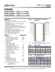
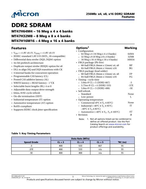
<strong>DDR2</strong> <strong>SDRAM</strong><br />
MT47H64M4 – 16 Meg x 4 x 4 banks<br />
MT47H32M8 – 8 Meg x 8 x 4 banks<br />
MT47H16M16 – 4 Meg x 16 x 4 banks<br />
Features<br />
• V DD = +1.8V ±0.1V, V DDQ = +1.8V ±0.1V<br />
• JEDEC-standard 1.8V I/O (SSTL_18-compatible)<br />
• Differential data strobe (DQS, DQS#) option<br />
• 4n-bit prefetch architecture<br />
• Duplicate output strobe (RDQS) option for <strong>x8</strong><br />
• DLL to align DQ and DQS transitions with CK<br />
• 4 internal banks for concurrent operation<br />
• Programmable CAS latency (CL)<br />
• Posted CAS additive latency (AL)<br />
• WRITE latency = READ latency - 1 t CK<br />
• Selectable burst lengths (BL): 4 or 8<br />
• Adjustable data-output drive strength<br />
• 64ms, 8192-cycle refresh<br />
• On-die termination (ODT)<br />
• Industrial temperature (IT) option<br />
• Automotive temperature (AT) option<br />
• RoHS-compliant<br />
• Supports JEDEC clock jitter specification<br />
Table 1: Key Timing Parameters<br />
PDF: 09005aef8117c187<br />
<strong>256Mb</strong><strong>DDR2</strong>.pdf - Rev. M 7/09 EN<br />
Speed Grade<br />
Options1 • Configuration<br />
Marking<br />
– 64 Meg x 4 (16 Meg x 4 x 4 banks) 64M4<br />
– 32 Meg x 8 (8 Meg x 8 x 4 banks) 32M8<br />
– 16 Meg x 16 (4 Meg x 16 x 4 banks)<br />
• FBGA package (Pb-free)<br />
16M16<br />
– 60-ball FBGA (8mm x 12mm) <strong>x4</strong>, <strong>x8</strong> BP<br />
– 84-ball FBGA (8mm x 14mm) <strong>x16</strong><br />
• FBGA package (lead solder)<br />
BG<br />
– 60-ball FBGA (8mm x 12mm) <strong>x4</strong>, <strong>x8</strong> FP<br />
– 84-ball FBGA (8mm x 14mm) <strong>x16</strong><br />
• Timing – cycle time<br />
FG<br />
– 3.0ns @ CL = 5 (<strong>DDR2</strong>-667) -3<br />
– 3.75ns @ CL = 4 (<strong>DDR2</strong>-533) -37E<br />
– 5.0ns @ CL = 3 (<strong>DDR2</strong>-400)<br />
• Self refresh<br />
-5E<br />
– Standard None<br />
– Low-power<br />
• Operating temperature<br />
L<br />
– Commercial (0°C ≤ TC ≤ 85°C) None<br />
– Industrial (–40°C ≤ TC ≤ 95°C;<br />
IT<br />
–40°C ≤ TA ≤ 85°C)<br />
– Automotive (–40°C ≤ TC, TA ≤ 105°C) AT<br />
• Revision :B<br />
Note: 1. Not all options listed can be combined to<br />
define an offered product. Use the Part<br />
Catalog Search on www.micron.com for<br />
product offerings and availability.<br />
Data Rate (MT/s)<br />
CL = 3 CL = 4 CL = 5<br />
<strong>256Mb</strong>: <strong>x4</strong>, <strong>x8</strong>, <strong>x16</strong> <strong>DDR2</strong> <strong>SDRAM</strong><br />
Features<br />
t RC (ns)<br />
-3 400 533 667 55<br />
-37E 400 533 n/a 55<br />
-5E 400 400 n/a 55<br />
1<br />
Products and specifications discussed herein are subject to change by <strong>Micron</strong> without notice.<br />
<strong>Micron</strong> Technology, Inc. reserves the right to change products or specifications without notice.<br />
©2003 <strong>Micron</strong> Technology, Inc. All rights reserved.
Table 2: Addressing<br />
Parameter 64 Meg x 4 32 Meg x 8 16 Meg x 16<br />
Configuration 16 Meg x 4 x 4 banks 8 Meg x 8 x 4 banks 4 Meg x 16 x 4 banks<br />
Refresh count 8K 8K 8K<br />
Row address A[12:0] (8K) A[12:0] (8K) A[12:0] (8K)<br />
Bank address BA[1:0] (4) BA[1:0] (4) BA[1:0] (4)<br />
Column address A[11, 9:0] (2K) A[9:0] (1K) A[8:0] (512)<br />
Figure 1: <strong>256Mb</strong> <strong>DDR2</strong> Part Numbers<br />
Configuration<br />
64 Meg x 4<br />
32 Meg x 8<br />
16 Meg x 16<br />
Example Part Number: MT47H32M8BP-3 :B<br />
MT47H Configuration Package Speed Revision<br />
Package<br />
Pb-free<br />
64M4<br />
32M8<br />
16M16<br />
84-ball 8mm x 14mm FBGA<br />
60-ball 8mm x 12mm FBGA<br />
Lead solder<br />
84-ball 8mm x 14mm FBGA<br />
60-ball 8mm x 12mm FBGA<br />
BG<br />
BP<br />
FG<br />
FP<br />
-<br />
-3<br />
-37E<br />
-5E<br />
{<br />
L<br />
IT<br />
:B<br />
Revision<br />
Speed Grade<br />
t CK = 3ns, CL = 5<br />
t CK = 3.75ns, CL = 4<br />
t CK = 5ns, CL = 3<br />
:<br />
Low power<br />
Industrial temperature<br />
AT Automotive temperature<br />
Note: 1. Not all speeds and configurations are available in all packages.<br />
FBGA Part Number System<br />
<strong>256Mb</strong>: <strong>x4</strong>, <strong>x8</strong>, <strong>x16</strong> <strong>DDR2</strong> <strong>SDRAM</strong><br />
Features<br />
Due to space limitations, FBGA-packaged components have an abbreviated part marking that is different from the<br />
part number. For a quick conversion of an FBGA code, see the FBGA Part Marking Decoder on <strong>Micron</strong>’s Web site:<br />
http://www.micron.com.<br />
PDF: 09005aef8117c187<br />
<strong>256Mb</strong><strong>DDR2</strong>.pdf - Rev. M 7/09 EN<br />
2<br />
<strong>Micron</strong> Technology, Inc. reserves the right to change products or specifications without notice.<br />
©2003 <strong>Micron</strong> Technology, Inc. All rights reserved.
<strong>256Mb</strong>: <strong>x4</strong>, <strong>x8</strong>, <strong>x16</strong> <strong>DDR2</strong> <strong>SDRAM</strong><br />
Contents<br />
State Diagram .................................................................................................................................................. 8<br />
Functional Description ..................................................................................................................................... 9<br />
Industrial Temperature ................................................................................................................................ 9<br />
Automotive Temperature ........................................................................................................................... 10<br />
General Notes ............................................................................................................................................ 10<br />
Functional Block Diagrams ............................................................................................................................. 11<br />
Ball Assignments and Descriptions ................................................................................................................. 13<br />
Packaging ...................................................................................................................................................... 17<br />
Package Dimensions .................................................................................................................................. 17<br />
FBGA Package Capacitance ......................................................................................................................... 19<br />
Electrical Specifications – Absolute Ratings ..................................................................................................... 20<br />
Temperature and Thermal Impedance ........................................................................................................ 20<br />
Electrical Specifications – I DD Parameters ........................................................................................................ 23<br />
I DD Specifications and Conditions ............................................................................................................... 23<br />
I DD7 Conditions .......................................................................................................................................... 23<br />
AC Timing Operating Specifications ................................................................................................................ 26<br />
AC and DC Operating Conditions .................................................................................................................... 37<br />
ODT DC Electrical Characteristics ................................................................................................................... 38<br />
Input Electrical Characteristics and Operating Conditions ............................................................................... 39<br />
Output Electrical Characteristics and Operating Conditions ............................................................................. 42<br />
Output Driver Characteristics ......................................................................................................................... 44<br />
Power and Ground Clamp Characteristics ....................................................................................................... 48<br />
AC Overshoot/Undershoot Specification ......................................................................................................... 49<br />
Input Slew Rate Derating ................................................................................................................................ 51<br />
Commands .................................................................................................................................................... 64<br />
Truth Tables ............................................................................................................................................... 64<br />
DESELECT ................................................................................................................................................. 68<br />
NO OPERATION (NOP) .............................................................................................................................. 69<br />
LOAD MODE (LM) ..................................................................................................................................... 69<br />
ACTIVATE .................................................................................................................................................. 69<br />
READ ......................................................................................................................................................... 69<br />
WRITE ....................................................................................................................................................... 69<br />
PRECHARGE .............................................................................................................................................. 70<br />
REFRESH ................................................................................................................................................... 70<br />
SELF REFRESH ........................................................................................................................................... 70<br />
Mode Register (MR) ........................................................................................................................................ 70<br />
Burst Length .............................................................................................................................................. 71<br />
Burst Type ................................................................................................................................................. 72<br />
Operating Mode ......................................................................................................................................... 72<br />
DLL RESET ................................................................................................................................................. 72<br />
Write Recovery ........................................................................................................................................... 73<br />
Power-Down Mode .................................................................................................................................... 73<br />
CAS Latency (CL) ........................................................................................................................................ 74<br />
Extended Mode Register (EMR) ....................................................................................................................... 75<br />
DLL Enable/Disable ................................................................................................................................... 76<br />
Output Drive Strength ................................................................................................................................ 76<br />
DQS# Enable/Disable ................................................................................................................................. 76<br />
RDQS Enable/Disable ................................................................................................................................. 76<br />
Output Enable/Disable ............................................................................................................................... 76<br />
On-Die Termination (ODT) ........................................................................................................................ 77<br />
PDF: 09005aef8117c187<br />
<strong>256Mb</strong><strong>DDR2</strong>.pdf - Rev. M 7/09 EN<br />
3<br />
<strong>Micron</strong> Technology, Inc. reserves the right to change products or specifications without notice.<br />
©2003 <strong>Micron</strong> Technology, Inc. All rights reserved.
<strong>256Mb</strong>: <strong>x4</strong>, <strong>x8</strong>, <strong>x16</strong> <strong>DDR2</strong> <strong>SDRAM</strong><br />
Off-Chip Driver (OCD) Impedance Calibration ............................................................................................ 77<br />
Posted CAS Additive Latency (AL) ............................................................................................................... 77<br />
Extended Mode Register 2 (EMR2) .................................................................................................................. 79<br />
Extended Mode Register 3 (EMR3) .................................................................................................................. 80<br />
Initialization .................................................................................................................................................. 81<br />
ACTIVATE ...................................................................................................................................................... 85<br />
READ ............................................................................................................................................................. 87<br />
READ with Precharge ................................................................................................................................. 91<br />
READ with Auto Precharge .......................................................................................................................... 93<br />
WRITE ........................................................................................................................................................... 98<br />
PRECHARGE ................................................................................................................................................. 108<br />
REFRESH ...................................................................................................................................................... 109<br />
SELF REFRESH .............................................................................................................................................. 110<br />
Power-Down Mode ....................................................................................................................................... 112<br />
Precharge Power-Down Clock Frequency Change .......................................................................................... 119<br />
Reset ............................................................................................................................................................. 120<br />
CKE Low Anytime ...................................................................................................................................... 120<br />
ODT Timing .................................................................................................................................................. 122<br />
MRS Command to ODT Update Delay ........................................................................................................ 124<br />
PDF: 09005aef8117c187<br />
<strong>256Mb</strong><strong>DDR2</strong>.pdf - Rev. M 7/09 EN<br />
4<br />
<strong>Micron</strong> Technology, Inc. reserves the right to change products or specifications without notice.<br />
©2003 <strong>Micron</strong> Technology, Inc. All rights reserved.
<strong>256Mb</strong>: <strong>x4</strong>, <strong>x8</strong>, <strong>x16</strong> <strong>DDR2</strong> <strong>SDRAM</strong><br />
List of Tables<br />
Table 1: Key Timing Parameters ...................................................................................................................... 1<br />
Table 2: Addressing ......................................................................................................................................... 2<br />
Table 3: FBGA 60-Ball – <strong>x4</strong>, <strong>x8</strong> and 84-Ball – <strong>x16</strong> Descriptions .......................................................................... 15<br />
Table 4: Input Capacitance ............................................................................................................................ 19<br />
Table 5: Absolute Maximum DC Ratings ........................................................................................................ 20<br />
Table 6: Temperature Limits .......................................................................................................................... 21<br />
Table 7: Thermal Impedance ......................................................................................................................... 22<br />
Table 8: General I DD Parameters .................................................................................................................... 23<br />
Table 9: I DD7 Timing Patterns (4-Bank Interleave READ Operation) ................................................................ 23<br />
Table 10: <strong>DDR2</strong> I DD Specifications and Conditions ......................................................................................... 24<br />
Table 11: AC Operating Specifications and Conditions .................................................................................... 26<br />
Table 12: Recommended DC Operating Conditions (SSTL_18) ........................................................................ 37<br />
Table 13: ODT DC Electrical Characteristics ................................................................................................... 38<br />
Table 14: Input DC Logic Levels ..................................................................................................................... 39<br />
Table 15: Input AC Logic Levels ..................................................................................................................... 39<br />
Table 16: Differential Input Logic Levels ........................................................................................................ 40<br />
Table 17: Differential AC Output Parameters .................................................................................................. 42<br />
Table 18: Output DC Current Drive ................................................................................................................ 42<br />
Table 19: Output Characteristics .................................................................................................................... 43<br />
Table 20: Full Strength Pull-Down Current (mA) ............................................................................................ 44<br />
Table 21: Full Strength Pull-Up Current (mA) ................................................................................................. 45<br />
Table 22: Reduced Strength Pull-Down Current (mA) ..................................................................................... 46<br />
Table 23: Reduced Strength Pull-Up Current (mA) .......................................................................................... 47<br />
Table 24: Input Clamp Characteristics ........................................................................................................... 48<br />
Table 25: Address and Control Balls ............................................................................................................... 49<br />
Table 26: Clock, Data, Strobe, and Mask Balls ................................................................................................. 49<br />
Table 27: AC Input Test Conditions ................................................................................................................ 50<br />
Table 28: <strong>DDR2</strong>-400/533 Setup and Hold Time Derating Values ( t IS and t IH) ................................................... 52<br />
Table 29: <strong>DDR2</strong>-667/800/1066 Setup and Hold Time Derating Values ( t IS and t IH) .......................................... 53<br />
Table 30: <strong>DDR2</strong>-400/533 t DS, t DH Derating Values with Differential Strobe ..................................................... 56<br />
Table 31: <strong>DDR2</strong>-667/800/1066 t DS, t DH Derating Values with Differential Strobe ............................................ 57<br />
Table 32: Single-Ended DQS Slew Rate Derating Values Using t DS b and t DH b .................................................. 58<br />
Table 33: Single-Ended DQS Slew Rate Fully Derated (DQS, DQ at V REF) at <strong>DDR2</strong>-667 ..................................... 58<br />
Table 34: Single-Ended DQS Slew Rate Fully Derated (DQS, DQ at V REF) at <strong>DDR2</strong>-533 ..................................... 59<br />
Table 35: Single-Ended DQS Slew Rate Fully Derated (DQS, DQ at V REF) at <strong>DDR2</strong>-400 ..................................... 59<br />
Table 36: Truth Table – <strong>DDR2</strong> Commands ..................................................................................................... 64<br />
Table 37: Truth Table – Current State Bank n – Command to Bank n ............................................................... 65<br />
Table 38: Truth Table – Current State Bank n – Command to Bank m .............................................................. 67<br />
Table 39: Minimum Delay with Auto Precharge Enabled ................................................................................. 68<br />
Table 40: Burst Definition .............................................................................................................................. 72<br />
Table 41: READ Using Concurrent Auto Precharge ......................................................................................... 93<br />
Table 42: WRITE Using Concurrent Auto Precharge ........................................................................................ 99<br />
Table 43: Truth Table – CKE ......................................................................................................................... 114<br />
PDF: 09005aef8117c187<br />
<strong>256Mb</strong><strong>DDR2</strong>.pdf - Rev. M 7/09 EN<br />
5<br />
<strong>Micron</strong> Technology, Inc. reserves the right to change products or specifications without notice.<br />
©2003 <strong>Micron</strong> Technology, Inc. All rights reserved.
<strong>256Mb</strong>: <strong>x4</strong>, <strong>x8</strong>, <strong>x16</strong> <strong>DDR2</strong> <strong>SDRAM</strong><br />
List of Figures<br />
Figure 1: <strong>256Mb</strong> <strong>DDR2</strong> Part Numbers .............................................................................................................. 2<br />
Figure 2: Simplified State Diagram ................................................................................................................... 8<br />
Figure 3: 64 Meg x 4 Functional Block Diagram .............................................................................................. 11<br />
Figure 4: 32 Meg x 8 Functional Block Diagram .............................................................................................. 12<br />
Figure 5: 16 Meg x 16 Functional Block Diagram ............................................................................................. 12<br />
Figure 6: 60-Ball FBGA – <strong>x4</strong>, <strong>x8</strong> Ball Assignments (Top View) ........................................................................... 13<br />
Figure 7: 84-Ball FBGA – <strong>x16</strong> Ball Assignments (Top View) .............................................................................. 14<br />
Figure 8: 84-Ball, FBGA Package (8mm x 14mm) – <strong>x16</strong> .................................................................................... 17<br />
Figure 9: 60-Ball, FBGA Package (8mm x 12mm) – <strong>x4</strong>, <strong>x8</strong> ................................................................................. 18<br />
Figure 10: Example Temperature Test Point Location ..................................................................................... 21<br />
Figure 11: Single-Ended Input Signal Levels ................................................................................................... 39<br />
Figure 12: Differential Input Signal Levels ...................................................................................................... 40<br />
Figure 13: Differential Output Signal Levels .................................................................................................... 42<br />
Figure 14: Output Slew Rate Load .................................................................................................................. 43<br />
Figure 15: Full Strength Pull-Down Characteristics ......................................................................................... 44<br />
Figure 16: Full Strength Pull-Up Characteristics ............................................................................................. 45<br />
Figure 17: Reduced Strength Pull-Down Characteristics ................................................................................. 46<br />
Figure 18: Reduced Strength Pull-Up Characteristics ...................................................................................... 47<br />
Figure 19: Input Clamp Characteristics .......................................................................................................... 48<br />
Figure 20: Overshoot ..................................................................................................................................... 49<br />
Figure 21: Undershoot .................................................................................................................................. 49<br />
Figure 22: Nominal Slew Rate for t IS .............................................................................................................. 54<br />
Figure 23: Tangent Line for t IS ....................................................................................................................... 54<br />
Figure 24: Nominal Slew Rate for t IH .............................................................................................................. 55<br />
Figure 25: Tangent Line for t IH ...................................................................................................................... 55<br />
Figure 26: Nominal Slew Rate for t DS ............................................................................................................. 60<br />
Figure 27: Tangent Line for t DS ...................................................................................................................... 60<br />
Figure 28: Nominal Slew Rate for t DH ............................................................................................................ 61<br />
Figure 29: Tangent Line for t DH ..................................................................................................................... 61<br />
Figure 30: AC Input Test Signal Waveform Command/Address Balls ............................................................... 62<br />
Figure 31: AC Input Test Signal Waveform for Data with DQS, DQS# (Differential) ........................................... 62<br />
Figure 32: AC Input Test Signal Waveform for Data with DQS (Single-Ended) .................................................. 63<br />
Figure 33: AC Input Test Signal Waveform (Differential) ................................................................................. 63<br />
Figure 34: MR Definition ............................................................................................................................... 71<br />
Figure 35: CL ................................................................................................................................................ 74<br />
Figure 36: EMR Definition ............................................................................................................................. 75<br />
Figure 37: READ Latency ............................................................................................................................... 78<br />
Figure 38: WRITE Latency ............................................................................................................................. 78<br />
Figure 39: EMR2 Definition ........................................................................................................................... 79<br />
Figure 40: EMR3 Definition ........................................................................................................................... 80<br />
Figure 41: <strong>DDR2</strong> Power-Up and Initialization ................................................................................................. 82<br />
Figure 42: Example: Meeting t RRD (MIN) and t RCD (MIN) .............................................................................. 85<br />
Figure 43: Multibank Activate Restriction ....................................................................................................... 86<br />
Figure 44: READ Latency ............................................................................................................................... 88<br />
Figure 45: Consecutive READ Bursts .............................................................................................................. 89<br />
Figure 46: Nonconsecutive READ Bursts ........................................................................................................ 90<br />
Figure 47: READ Interrupted by READ ........................................................................................................... 91<br />
Figure 48: READ-to-WRITE ............................................................................................................................ 91<br />
Figure 49: READ-to-PRECHARGE – BL = 4 ...................................................................................................... 92<br />
Figure 50: READ-to-PRECHARGE – BL = 8 ...................................................................................................... 92<br />
PDF: 09005aef8117c187<br />
<strong>256Mb</strong><strong>DDR2</strong>.pdf - Rev. M 7/09 EN<br />
6<br />
<strong>Micron</strong> Technology, Inc. reserves the right to change products or specifications without notice.<br />
©2003 <strong>Micron</strong> Technology, Inc. All rights reserved.
<strong>256Mb</strong>: <strong>x4</strong>, <strong>x8</strong>, <strong>x16</strong> <strong>DDR2</strong> <strong>SDRAM</strong><br />
Figure 51: Bank Read – Without Auto Precharge ............................................................................................. 94<br />
Figure 52: Bank Read – with Auto Precharge ................................................................................................... 95<br />
Figure 53: <strong>x4</strong>, <strong>x8</strong> Data Output Timing – t DQSQ, t QH, and Data Valid Window .................................................. 96<br />
Figure 54: <strong>x16</strong> Data Output Timing – t DQSQ, t QH, and Data Valid Window ...................................................... 97<br />
Figure 55: Data Output Timing – t AC and t DQSCK .......................................................................................... 98<br />
Figure 56: Write Burst ................................................................................................................................... 100<br />
Figure 57: Consecutive WRITE-to-WRITE ...................................................................................................... 101<br />
Figure 58: Nonconsecutive WRITE-to-WRITE ................................................................................................ 101<br />
Figure 59: WRITE Interrupted by WRITE ....................................................................................................... 102<br />
Figure 60: WRITE-to-READ ........................................................................................................................... 103<br />
Figure 61: WRITE-to-PRECHARGE ................................................................................................................ 104<br />
Figure 62: Bank Write – Without Auto Precharge ............................................................................................ 105<br />
Figure 63: Bank Write – with Auto Precharge ................................................................................................. 106<br />
Figure 64: WRITE – DM Operation ................................................................................................................ 107<br />
Figure 65: Data Input Timing ........................................................................................................................ 108<br />
Figure 66: Refresh Mode ............................................................................................................................... 109<br />
Figure 67: Self Refresh .................................................................................................................................. 111<br />
Figure 68: Power-Down ................................................................................................................................ 113<br />
Figure 69: READ-to-Power-Down or Self Refresh Entry .................................................................................. 115<br />
Figure 70: READ with Auto Precharge-to-Power-Down or Self Refresh Entry .................................................. 115<br />
Figure 71: WRITE-to-Power-Down or Self Refresh Entry ................................................................................ 116<br />
Figure 72: WRITE with Auto Precharge-to-Power-Down or Self Refresh Entry ................................................. 116<br />
Figure 73: REFRESH Command-to-Power-Down Entry ................................................................................. 117<br />
Figure 74: ACTIVATE Command-to-Power-Down Entry ................................................................................ 117<br />
Figure 75: PRECHARGE Command-to-Power-Down Entry ............................................................................ 118<br />
Figure 76: LOAD MODE Command-to-Power-Down Entry ............................................................................ 118<br />
Figure 77: Input Clock Frequency Change During Precharge Power-Down Mode ........................................... 119<br />
Figure 78: RESET Function ........................................................................................................................... 121<br />
Figure 79: ODT Timing for Entering and Exiting Power-Down Mode .............................................................. 123<br />
Figure 80: Timing for MRS Command to ODT Update Delay .......................................................................... 124<br />
Figure 81: ODT Timing for Active or Fast-Exit Power-Down Mode ................................................................. 124<br />
Figure 82: ODT Timing for Slow-Exit or Precharge Power-Down Modes ......................................................... 125<br />
Figure 83: ODT Turn-Off Timings When Entering Power-Down Mode ............................................................ 125<br />
Figure 84: ODT Turn-On Timing When Entering Power-Down Mode ............................................................. 126<br />
Figure 85: ODT Turn-Off Timing When Exiting Power-Down Mode ............................................................... 127<br />
Figure 86: ODT Turn-On Timing When Exiting Power-Down Mode ................................................................ 128<br />
PDF: 09005aef8117c187<br />
<strong>256Mb</strong><strong>DDR2</strong>.pdf - Rev. M 7/09 EN<br />
7<br />
<strong>Micron</strong> Technology, Inc. reserves the right to change products or specifications without notice.<br />
©2003 <strong>Micron</strong> Technology, Inc. All rights reserved.
State Diagram<br />
Figure 2: Simplified State Diagram<br />
PDF: 09005aef8117c187<br />
<strong>256Mb</strong><strong>DDR2</strong>.pdf - Rev. M 7/09 EN<br />
OCD<br />
default<br />
Setting<br />
MRS<br />
EMRS<br />
(E)MRS<br />
CKE_L<br />
Writing<br />
WRITE A<br />
Writing<br />
with<br />
auto<br />
precharge<br />
PRE<br />
Automatic Sequence<br />
Command Sequence<br />
Active<br />
powerdown<br />
WRITE<br />
CKE_L<br />
CKE_L<br />
CKE_H<br />
Initialization<br />
sequence<br />
Idle<br />
all banks<br />
precharged<br />
WRITE A<br />
WRITE<br />
READ A<br />
ACT<br />
Activating<br />
Bank<br />
active<br />
PRE, PRE_A<br />
Precharging<br />
CKE_H<br />
READ A<br />
WRITE A<br />
PRE , PRE_A<br />
CKE_H<br />
CKE_L<br />
READ<br />
READ<br />
SR<br />
Precharge<br />
powerdown<br />
Reading<br />
CKE_L<br />
Self<br />
refreshing<br />
REFRESH<br />
READ A<br />
Reading<br />
with<br />
auto<br />
precharge<br />
CKE_L<br />
CKE_L<br />
WRITE READ<br />
PRE, PRE_A<br />
<strong>256Mb</strong>: <strong>x4</strong>, <strong>x8</strong>, <strong>x16</strong> <strong>DDR2</strong> <strong>SDRAM</strong><br />
State Diagram<br />
Refreshing<br />
ACT = ACTIVATE<br />
CKE_H = CKE HIGH, exit power-down or self refresh<br />
CKE_L = CKE LOW, enter power-down<br />
(E)MRS = (Extended) mode register set<br />
PRE = PRECHARGE<br />
PRE_A = PRECHARGE ALL<br />
READ = READ<br />
READ A = READ with auto precharge<br />
REFRESH = REFRESH<br />
SR = SELF REFRESH<br />
WRITE = WRITE<br />
WRITE A = WRITE with auto precharge<br />
Note: 1. This diagram provides the basic command flow. It is not comprehensive and does not<br />
identify all timing requirements or possible command restrictions such as multibank interaction,<br />
power down, entry/exit, etc.<br />
8<br />
<strong>Micron</strong> Technology, Inc. reserves the right to change products or specifications without notice.<br />
©2003 <strong>Micron</strong> Technology, Inc. All rights reserved.
Functional Description<br />
Industrial Temperature<br />
PDF: 09005aef8117c187<br />
<strong>256Mb</strong><strong>DDR2</strong>.pdf - Rev. M 7/09 EN<br />
<strong>256Mb</strong>: <strong>x4</strong>, <strong>x8</strong>, <strong>x16</strong> <strong>DDR2</strong> <strong>SDRAM</strong><br />
Functional Description<br />
The <strong>DDR2</strong> <strong>SDRAM</strong> uses a double data rate architecture to achieve high-speed operation.<br />
The double data rate architecture is essentially a 4n-prefetch architecture, with an<br />
interface designed to transfer two data words per clock cycle at the I/O balls. A single<br />
read or write access for the <strong>DDR2</strong> <strong>SDRAM</strong> effectively consists of a single 4n-bit-wide, oneclock-cycle<br />
data transfer at the internal DRAM core and four corresponding n-bit-wide,<br />
one-half-clock-cycle data transfers at the I/O balls.<br />
A bidirectional data strobe (DQS, DQS#) is transmitted externally, along with data, for<br />
use in data capture at the receiver. DQS is a strobe transmitted by the <strong>DDR2</strong> <strong>SDRAM</strong><br />
during READs and by the memory controller during WRITEs. DQS is edge-aligned with<br />
data for READs and center-aligned with data for WRITEs. The <strong>x16</strong> offering has two data<br />
strobes, one for the lower byte (LDQS, LDQS#) and one for the upper byte (UDQS, UDQS#).<br />
The <strong>DDR2</strong> <strong>SDRAM</strong> operates from a differential clock (CK and CK#); the crossing of CK<br />
going HIGH and CK# going LOW will be referred to as the positive edge of CK. Commands<br />
(address and control signals) are registered at every positive edge of CK. Input<br />
data is registered on both edges of DQS, and output data is referenced to both edges of<br />
DQS as well as to both edges of CK.<br />
Read and write accesses to the <strong>DDR2</strong> <strong>SDRAM</strong> are burst-oriented; accesses start at a selected<br />
location and continue for a programmed number of locations in a programmed<br />
sequence. Accesses begin with the registration of an ACTIVATE command, which is<br />
then followed by a READ or WRITE command. The address bits registered coincident<br />
with the ACTIVATE command are used to select the bank and row to be accessed. The<br />
address bits registered coincident with the READ or WRITE command are used to select<br />
the bank and the starting column location for the burst access.<br />
The <strong>DDR2</strong> <strong>SDRAM</strong> provides for programmable read or write burst lengths of four or<br />
eight locations. <strong>DDR2</strong> <strong>SDRAM</strong> supports interrupting a burst read of eight with another<br />
read or a burst write of eight with another write. An auto precharge function may be<br />
enabled to provide a self-timed row precharge that is initiated at the end of the burst<br />
access.<br />
As with standard DDR <strong>SDRAM</strong>, the pipelined, multibank architecture of <strong>DDR2</strong> <strong>SDRAM</strong><br />
enables concurrent operation, thereby providing high, effective bandwidth by hiding<br />
row precharge and activation time.<br />
A self refresh mode is provided, along with a power-saving, power-down mode.<br />
All inputs are compatible with the JEDEC standard for SSTL_18. All full drive-strength<br />
outputs are SSTL_18-compatible.<br />
The industrial temperature (IT) option, if offered, has two simultaneous requirements:<br />
ambient temperature surrounding the device cannot be less than –40°C or greater than<br />
+85°C, and the case temperature cannot be less than –40°C or greater than +95°C. JE-<br />
DEC specifications require the refresh rate to double when T C exceeds +85°C; this also<br />
requires use of the high-temperature self refresh option. Additionally, ODT resistance<br />
and the input/output impedance must be derated when T C is < 0°C or > +85°C.<br />
9<br />
<strong>Micron</strong> Technology, Inc. reserves the right to change products or specifications without notice.<br />
©2003 <strong>Micron</strong> Technology, Inc. All rights reserved.
Automotive Temperature<br />
General Notes<br />
PDF: 09005aef8117c187<br />
<strong>256Mb</strong><strong>DDR2</strong>.pdf - Rev. M 7/09 EN<br />
<strong>256Mb</strong>: <strong>x4</strong>, <strong>x8</strong>, <strong>x16</strong> <strong>DDR2</strong> <strong>SDRAM</strong><br />
Functional Description<br />
The automotive temperature (AT) option, if offered, has two simultaneous requirements:<br />
ambient temperature surrounding the device cannot be less than –40°C or<br />
greater than +105°C, and the case temperature cannot be less than –40°C or greater<br />
than +105°C. JEDEC specifications require the refresh rate to double when T C exceeds<br />
+85°C; this also requires use of the high-temperature self refresh option. Additionally,<br />
ODT resistance and the input/output impedance must be derated when T C is < 0°C or ><br />
+85°C.<br />
• The functionality and the timing specifications discussed in this data sheet are for the<br />
DLL-enabled mode of operation.<br />
• Throughout the data sheet, the various figures and text refer to DQs as “DQ.” The DQ<br />
term is to be interpreted as any and all DQ collectively, unless specifically stated otherwise.<br />
Additionally, the <strong>x16</strong> is divided into 2 bytes: the lower byte and the upper byte.<br />
For the lower byte (DQ0–DQ7), DM refers to LDM and DQS refers to LDQS. For the<br />
upper byte (DQ8–DQ15), DM refers to UDM and DQS refers to UDQS.<br />
• Complete functionality is described throughout the document, and any page or diagram<br />
may have been simplified to convey a topic and may not be inclusive of all<br />
requirements.<br />
• Any specific requirement takes precedence over a general statement.<br />
10<br />
<strong>Micron</strong> Technology, Inc. reserves the right to change products or specifications without notice.<br />
©2003 <strong>Micron</strong> Technology, Inc. All rights reserved.
Functional Block Diagrams<br />
The <strong>DDR2</strong> <strong>SDRAM</strong> is a high-speed CMOS, dynamic random access memory. It is internally<br />
configured as a multibank DRAM.<br />
Figure 3: 64 Meg x 4 Functional Block Diagram<br />
ODT<br />
CKE<br />
CK<br />
CK#<br />
CS#<br />
RAS#<br />
CAS#<br />
WE#<br />
A0–A12,<br />
BA0–BA1<br />
Command<br />
decode<br />
Control<br />
logic<br />
Mode<br />
registers<br />
Address<br />
15 register<br />
PDF: 09005aef8117c187<br />
<strong>256Mb</strong><strong>DDR2</strong>.pdf - Rev. M 7/09 EN<br />
15<br />
Refresh<br />
13<br />
counter Row- 13<br />
address<br />
MUX<br />
13<br />
11<br />
2<br />
2<br />
Bank<br />
control<br />
logic<br />
Columnaddress<br />
counter/<br />
latch<br />
Bank 3<br />
Bank 2<br />
Bank 1<br />
Bank 0<br />
row-<br />
address 8,192<br />
latch and<br />
decoder<br />
9<br />
2<br />
Bank 3<br />
Bank 2<br />
Bank 1<br />
Bank 0<br />
memory<br />
array<br />
(8,192 x 512 x 16)<br />
Sense amplifiers<br />
8,192<br />
I/O gating<br />
DM mask logic<br />
512<br />
(<strong>x16</strong>)<br />
Column<br />
decoder<br />
16<br />
READ<br />
latch<br />
Column 0, Column 1<br />
Column 0, Column 1<br />
4<br />
4<br />
4<br />
4<br />
MUX<br />
4<br />
Data<br />
DQS<br />
generator<br />
16<br />
Input<br />
registers<br />
1 1<br />
4<br />
1<br />
WRITE<br />
FIFO Mask 1<br />
1<br />
1<br />
16 and 1 1<br />
Internal<br />
CK, CK#<br />
drivers<br />
CK out<br />
4<br />
16 4<br />
4<br />
4<br />
CK in<br />
Data 4 4<br />
11<br />
<strong>256Mb</strong>: <strong>x4</strong>, <strong>x8</strong>, <strong>x16</strong> <strong>DDR2</strong> <strong>SDRAM</strong><br />
Functional Block Diagrams<br />
4<br />
2<br />
CK, CK#<br />
DLL<br />
DRVRS<br />
DQS, DQS#<br />
4<br />
1<br />
4<br />
2<br />
RCVRS<br />
ODT control Vdd Q<br />
sw1 sw2 sw3<br />
sw1 sw2<br />
R1<br />
R1<br />
R2<br />
R2<br />
sw1 sw2<br />
R1<br />
R1<br />
R2<br />
R2<br />
sw1 sw2<br />
R1<br />
R1<br />
R2<br />
R2<br />
VssQ<br />
sw3<br />
R3<br />
R3<br />
sw3<br />
R3<br />
R3<br />
sw3<br />
R3<br />
R3<br />
DQ0–DQ3<br />
DQS, DQS#<br />
<strong>Micron</strong> Technology, Inc. reserves the right to change products or specifications without notice.<br />
©2003 <strong>Micron</strong> Technology, Inc. All rights reserved.<br />
DM
Figure 4: 32 Meg x 8 Functional Block Diagram<br />
ODT<br />
CKE<br />
CK<br />
CK#<br />
CS#<br />
RAS#<br />
CAS#<br />
WE#<br />
A0–A12,<br />
BA0–BA1<br />
Command<br />
decode<br />
Control<br />
logic<br />
Mode<br />
registers<br />
15<br />
Address<br />
15 register<br />
Bank 3<br />
Bank 2<br />
Bank 1<br />
Refresh 13 Row-<br />
Bank 0<br />
counter<br />
13<br />
rowaddressaddress<br />
MUX<br />
8,192<br />
latch and<br />
13<br />
decoder<br />
10<br />
2<br />
2<br />
Bank<br />
control<br />
logic<br />
Columnaddress<br />
counter/<br />
latch<br />
8<br />
2<br />
Bank 3<br />
Bank 2<br />
Bank 1<br />
Bank 0<br />
Memory<br />
array<br />
(8,192 x 256 x 32)<br />
Sense amplifiers<br />
8,192<br />
I/O gating<br />
DM mask logic<br />
256<br />
(x32)<br />
Column<br />
decoder<br />
Figure 5: 16 Meg x 16 Functional Block Diagram<br />
ODT<br />
CKE<br />
CK<br />
CK#<br />
CS#<br />
RAS#<br />
CAS#<br />
WE#<br />
A0–A12,<br />
BA0–BA1<br />
Command<br />
decode<br />
Control<br />
logic<br />
Mode<br />
registers<br />
Address<br />
15<br />
register<br />
PDF: 09005aef8117c187<br />
<strong>256Mb</strong><strong>DDR2</strong>.pdf - Rev. M 7/09 EN<br />
15<br />
Refresh<br />
13<br />
counter<br />
13<br />
9<br />
2<br />
Rowaddress<br />
MUX<br />
2<br />
13<br />
Bank<br />
control<br />
logic<br />
Columnaddress<br />
counter/<br />
latch<br />
Bank 3<br />
Bank 2<br />
Bank 1<br />
Bank 0<br />
rowaddress<br />
8,192<br />
latch and<br />
decoder<br />
7<br />
2<br />
Bank 3<br />
Bank 2<br />
Bank 1<br />
Bank 0<br />
Memory<br />
array<br />
(8,192 x 128 x 64)<br />
Sense amplifiers<br />
8,192<br />
I/O gating<br />
DM mask logic<br />
128<br />
(x64)<br />
Column<br />
decoder<br />
32<br />
READ<br />
latch<br />
Column 0, Column 1<br />
Column 0, Column 1<br />
8<br />
8<br />
8<br />
8<br />
MUX<br />
8<br />
Data<br />
DQS<br />
generator<br />
Input<br />
registers<br />
1 1<br />
32<br />
4<br />
1<br />
WRITE<br />
FIFO Mask 1<br />
1<br />
1<br />
32 and 1 1<br />
Internal<br />
CK, CK#<br />
drivers<br />
CK out<br />
8<br />
32 8<br />
8<br />
8<br />
CK in<br />
Data 8 8<br />
64<br />
Column 0, Column 1<br />
READ<br />
latch<br />
8<br />
8<br />
Column 0, Column 1<br />
16<br />
16<br />
16 MUX<br />
16<br />
2<br />
CK, CK#<br />
DLL<br />
DRVRS<br />
DQS, DQS#<br />
16<br />
Data<br />
1<br />
8<br />
RCVRS<br />
2<br />
CK, CK#<br />
DLL<br />
DQS<br />
4<br />
generator UDQS, UDQS#<br />
Input<br />
registers<br />
LDQS, LDQS#<br />
64<br />
2 2<br />
2 2<br />
WRITE<br />
8<br />
2 2 2<br />
FIFO<br />
64 and<br />
drivers<br />
Internal<br />
CK out<br />
CK, CK#<br />
CK in<br />
Mask<br />
64<br />
Data<br />
2<br />
16<br />
16<br />
16<br />
16<br />
2<br />
16<br />
16<br />
16<br />
16<br />
16<br />
RCVRS<br />
12<br />
<strong>256Mb</strong>: <strong>x4</strong>, <strong>x8</strong>, <strong>x16</strong> <strong>DDR2</strong> <strong>SDRAM</strong><br />
Functional Block Diagrams<br />
DRVRS<br />
4<br />
ODT control Vdd Q<br />
sw1 sw2 sw3<br />
sw1 sw2<br />
R1<br />
R1<br />
R1<br />
R1<br />
R2<br />
R2<br />
sw1 sw2<br />
R1<br />
R1<br />
R2<br />
R2<br />
sw1 sw2<br />
R2<br />
R2<br />
VssQ<br />
sw3<br />
R3<br />
R3<br />
sw3<br />
R3<br />
R3<br />
sw3<br />
R3<br />
R3<br />
ODT control Vdd Q<br />
sw1 sw2 sw3<br />
sw1 sw2<br />
R1<br />
R1<br />
R2<br />
R2<br />
sw1 sw2<br />
R1<br />
R1<br />
R2<br />
R2<br />
sw1 sw2<br />
R1<br />
R1<br />
R2<br />
R2<br />
VssQ<br />
sw3<br />
R3<br />
R3<br />
sw3<br />
R3<br />
R3<br />
sw3<br />
R3<br />
R3<br />
DQ0–DQ7<br />
DQS, DQS#<br />
RDQS#<br />
RDQS<br />
DM<br />
DQ0–DQ15<br />
UDQS, UDQS#<br />
LDQS, LDQS#<br />
UDM, LDM<br />
<strong>Micron</strong> Technology, Inc. reserves the right to change products or specifications without notice.<br />
©2003 <strong>Micron</strong> Technology, Inc. All rights reserved.
Ball Assignments and Descriptions<br />
Figure 6: 60-Ball FBGA – <strong>x4</strong>, <strong>x8</strong> Ball Assignments (Top View)<br />
PDF: 09005aef8117c187<br />
<strong>256Mb</strong><strong>DDR2</strong>.pdf - Rev. M 7/09 EN<br />
A<br />
B<br />
C<br />
D<br />
E<br />
F<br />
G<br />
H<br />
J<br />
K<br />
L<br />
1 2 3 4 5 6 7 8 9<br />
V DD<br />
NF, DQ6<br />
V DDQ<br />
NF, DQ4<br />
V DDL<br />
RFU<br />
V SS<br />
V DD<br />
NF, RDQS#/NU<br />
VSSQ DM, DM/RDQS<br />
DQ1<br />
V SSQ<br />
V REF<br />
CKE<br />
BA0<br />
A10<br />
A3<br />
A7<br />
A12<br />
V SS<br />
V DDQ<br />
DQ3<br />
V SS<br />
WE#<br />
BA1<br />
A1<br />
A5<br />
A9<br />
RFU<br />
13<br />
<strong>256Mb</strong>: <strong>x4</strong>, <strong>x8</strong>, <strong>x16</strong> <strong>DDR2</strong> <strong>SDRAM</strong><br />
Ball Assignments and Descriptions<br />
V SSQ<br />
DQS<br />
V DDQ<br />
DQ2<br />
V SSDL<br />
RAS#<br />
CAS#<br />
A2<br />
A6<br />
A11<br />
RFU<br />
DQS#/NU<br />
V SSQ<br />
DQ0<br />
V SSQ<br />
CK<br />
CK#<br />
CS#<br />
A0<br />
A4<br />
A8<br />
RFU<br />
V DDQ<br />
NF, DQ7<br />
V DDQ<br />
NF, DQ5<br />
V DD<br />
ODT<br />
V DD<br />
V SS<br />
<strong>Micron</strong> Technology, Inc. reserves the right to change products or specifications without notice.<br />
©2003 <strong>Micron</strong> Technology, Inc. All rights reserved.
Figure 7: 84-Ball FBGA – <strong>x16</strong> Ball Assignments (Top View)<br />
PDF: 09005aef8117c187<br />
<strong>256Mb</strong><strong>DDR2</strong>.pdf - Rev. M 7/09 EN<br />
A<br />
B<br />
C<br />
D<br />
E<br />
F<br />
G<br />
H<br />
J<br />
K<br />
L<br />
M<br />
N<br />
P<br />
R<br />
1 2 3 4 5 6 7 8 9<br />
V DD<br />
DQ14<br />
V DDQ<br />
DQ12<br />
V DD<br />
DQ6<br />
V DDQ<br />
DQ4<br />
V DDL<br />
RFU<br />
V SS<br />
V DD<br />
NC<br />
V SSQ<br />
DQ9<br />
V SSQ<br />
NC<br />
V SSQ<br />
DQ1<br />
V SSQ<br />
V REF<br />
CKE<br />
BA0<br />
A10<br />
A3<br />
A7<br />
A12<br />
V SS<br />
UDM<br />
V DDQ<br />
DQ11<br />
V SS<br />
LDM<br />
V DDQ<br />
DQ3<br />
V SS<br />
WE#<br />
BA1<br />
A1<br />
A5<br />
A9<br />
RFU<br />
14<br />
<strong>256Mb</strong>: <strong>x4</strong>, <strong>x8</strong>, <strong>x16</strong> <strong>DDR2</strong> <strong>SDRAM</strong><br />
Ball Assignments and Descriptions<br />
VSSQ UDQS#/NU VDDQ UDQS<br />
V DDQ<br />
DQ10<br />
V SSQ<br />
LDQS<br />
V DDQ<br />
DQ2<br />
V SSDL<br />
RAS#<br />
CAS#<br />
A2<br />
A6<br />
A11<br />
RFU<br />
V SSQ<br />
DQ8<br />
V SSQ<br />
LDQS#/NU<br />
V SSQ<br />
DQ0<br />
V SSQ<br />
CK<br />
CK#<br />
CS#<br />
A0<br />
A4<br />
A8<br />
RFU<br />
DQ15<br />
V DDQ<br />
DQ13<br />
V DDQ<br />
DQ7<br />
V DDQ<br />
DQ5<br />
V DD<br />
ODT<br />
V DD<br />
V SS<br />
<strong>Micron</strong> Technology, Inc. reserves the right to change products or specifications without notice.<br />
©2003 <strong>Micron</strong> Technology, Inc. All rights reserved.
Table 3: FBGA 60-Ball – <strong>x4</strong>, <strong>x8</strong> and 84-Ball – <strong>x16</strong> Descriptions<br />
Symbol Type Description<br />
A[12:0] Input Address inputs: Provide the row address for ACTIVE commands, and the column address<br />
and auto precharge bit (A10) for READ/WRITE commands, to select one location out of the<br />
memory array in the respective bank. A10 sampled during a PRECHARGE command determines<br />
whether the PRECHARGE applies to one bank (A10 LOW, bank selected by BA[1:0]) or<br />
all banks (A10 HIGH). The address inputs also provide the op-code during a LOAD MODE<br />
command.<br />
BA0, BA1 Input Bank address inputs: BA[1:0] define to which bank an ACTIVATE, READ, WRITE, or PRE-<br />
CHARGE command is being applied. BA[1:0] define which mode register, including MR,<br />
EMR, EMR(2), and EMR(3), is loaded during the LOAD MODE command.<br />
CK, CK# Input Clock: CK and CK# are differential clock inputs. All control, command, and address input<br />
signals are sampled on the crossing of the positive edge of CK and negative edge of CK#.<br />
Output data (DQ and DQS/DQS#) is referenced to the crossings of CK and CK#.<br />
CKE Input Clock enable: CKE enables (registered HIGH) and disables (registered LOW) internal circuitry<br />
and clocks on the <strong>DDR2</strong> <strong>SDRAM</strong>. The specific circuitry that is enabled/disabled is dependent<br />
on the <strong>DDR2</strong> <strong>SDRAM</strong> configuration and operating mode. Taking CKE LOW provides<br />
precharge power-down and SELF REFRESH operations (all banks idle), or ACTIVATE powerdown<br />
(row active in any bank). CKE is synchronous for power-down entry, power-down exit,<br />
output disable, and self refresh entry. CKE is asynchronous for self refresh exit. Input buffers<br />
(excluding CK, CK#, CKE, and ODT) are disabled during power-down. Input buffers (excluding<br />
CKE) are disabled during SELF REFRESH. CKE is an SSTL_18 input but will detect a<br />
LVCMOS LOW level once V DD is applied during first power-up. After V REF has become stable<br />
during the power-on and initialization sequence, it must be maintained for proper operation<br />
of the CKE receiver. For proper SELF-REFRESH operation, V REF must be maintained.<br />
CS# Input Chip select: CS# enables (registered LOW) and disables (registered HIGH) the command decoder.<br />
All commands are masked when CS# is registered high. CS# provides for external<br />
bank selection on systems with multiple ranks. CS# is considered part of the command code.<br />
LDM, UDM, DM Input Input data mask: DM is an input mask signal for write data. Input data is masked when<br />
DM is sampled HIGH, along with the input data, during a write access. DM is sampled on<br />
both edges of DQS. Although DM balls are input-only, the DM loading is designed to match<br />
that of DQ and DQS balls. LDM is DM for the lower byte DQ[7:0], and UDM is DM for the<br />
upper byte DQ[15:8].<br />
ODT Input On-die termination: ODT enables (registered HIGH) and disables (registered LOW) termination<br />
resistance internal to the <strong>DDR2</strong> <strong>SDRAM</strong>. When enabled, ODT is only applied to each of<br />
the following balls for the <strong>x4</strong> configuration: DQ[3:0], DQS, DQS#, and DM; for the <strong>x8</strong> configuration:<br />
DQ[7:0], DQS, DQS#, RDQS, RDQS#, and DM; and for the <strong>x16</strong> configuration:<br />
DQ[15:0], LDM, UDM, LDQS, LDQS#, UDQS, and UDQS#. The ODT input will be ignored if<br />
disabled via the LOAD MODE command.<br />
RAS#, CAS#,<br />
WE#<br />
DQ[15:0] (<strong>x16</strong>)<br />
DQ[3:0] (<strong>x4</strong>)<br />
DQ[7:0] (<strong>x8</strong>)<br />
<strong>256Mb</strong>: <strong>x4</strong>, <strong>x8</strong>, <strong>x16</strong> <strong>DDR2</strong> <strong>SDRAM</strong><br />
Ball Assignments and Descriptions<br />
Input Command inputs: RAS#, CAS#, and WE# (along with CS#) define the command being entered.<br />
I/O Data input/output: Bidirectional data bus for the 16 Meg x 16 configuration.<br />
Bidirectional data bus for the 64 Meg x 4 configuration.<br />
Bidirectional data bus for the 32 Meg x 8 configuration.<br />
DQS, DQS# I/O Data strobe: DQS# is only used when differential data strobe mode is enabled via the<br />
LOAD MODE command. Output with read data. Edge-aligned with read data. Input with<br />
write data. Center-aligned with write data.<br />
PDF: 09005aef8117c187<br />
<strong>256Mb</strong><strong>DDR2</strong>.pdf - Rev. M 7/09 EN<br />
15<br />
<strong>Micron</strong> Technology, Inc. reserves the right to change products or specifications without notice.<br />
©2003 <strong>Micron</strong> Technology, Inc. All rights reserved.
Table 3: FBGA 60-Ball – <strong>x4</strong>, <strong>x8</strong> and 84-Ball – <strong>x16</strong> Descriptions (Continued)<br />
Symbol Type Description<br />
LDQS, LDQS# I/O Data strobe for lower byte: LDQS# is only used when differential data strobe mode is<br />
enabled via the LOAD MODE command. Output with read data. Edge-aligned with read data.<br />
Input with write data. Center-aligned with write data.<br />
UDQS, UDQS# I/O Data strobe for upper byte: UDQS# is only used when differential data strobe mode is<br />
enabled via the LOAD MODE command. Output with read data. Edge-aligned with read data.<br />
Input with write data. Center-aligned with write data.<br />
RDQS, RDQS# Output Redundant data strobe: For the <strong>x8</strong> configuration only. RDQS is enabled/disabled via the<br />
LOAD MODE command to the extended mode register (EMR). When RDQS is enabled, RDQS<br />
is output with read data only and is ignored during write data. When RDQS is disabled, ball<br />
B3 becomes data mask (see DM ball). RDQS# is only used when RDQS is enabled and differential<br />
data strobe mode is enabled.<br />
V DD Supply Power supply: 1.8V ±0.1V.<br />
V DDL Supply DLL power supply: 1.8V ±0.1V.<br />
V DDQ Supply DQ power supply: 1.8V ±0.1V. Isolated on the device for improved noise immunity.<br />
V REF Supply SSTL_18 reference voltage (V DDQ/2).<br />
V SS Supply Ground.<br />
V SSDL Supply DLL ground: Isolated on the device from V SS and V SSQ.<br />
V SSQ Supply DQ ground: Isolated on the device for improved noise immunity.<br />
NC – No connect: These balls should be left unconnected.<br />
<strong>256Mb</strong>: <strong>x4</strong>, <strong>x8</strong>, <strong>x16</strong> <strong>DDR2</strong> <strong>SDRAM</strong><br />
Ball Assignments and Descriptions<br />
NF – No function: For the <strong>x4</strong> configuration, these balls are no function. For the <strong>x8</strong> configuration,<br />
they are used as DQ[7:4].<br />
NU – Not used: If EMR(E10) = 0: For the <strong>x4</strong> configuration, A2 = NU and A8 = NU. For the <strong>x8</strong> configuration,<br />
A2 = RDQS# and A8 = DQS#. If EMR(E10) = 1: For the <strong>x4</strong> configuration, A2 = NU<br />
and A8 = NU. For the <strong>x8</strong> configuration, A2 = NU and A8 = NU.<br />
NU – Not Used: If EMR(E10) = 0: For the <strong>x16</strong> configuration, A8 = UDQS# and E8 = LDQS#. If<br />
EMR(E10) = 1: For the <strong>x16</strong> configuration, A8 = NU and E8 = NU.<br />
RFU – Reserved for future use: Bank address BA2, row address bits A[15:13].<br />
PDF: 09005aef8117c187<br />
<strong>256Mb</strong><strong>DDR2</strong>.pdf - Rev. M 7/09 EN<br />
16<br />
<strong>Micron</strong> Technology, Inc. reserves the right to change products or specifications without notice.<br />
©2003 <strong>Micron</strong> Technology, Inc. All rights reserved.
Packaging<br />
Package Dimensions<br />
Figure 8: 84-Ball, FBGA Package (8mm x 14mm) – <strong>x16</strong><br />
Seating plane<br />
84X Ø0.45<br />
Solder ball material:<br />
Pb-free – (SAC305) SnAgCu<br />
Pb – (Eutectic) SnPbAg<br />
Dimensions apply to solder<br />
balls post-reflow.<br />
PDF: 09005aef8117c187<br />
<strong>256Mb</strong><strong>DDR2</strong>.pdf - Rev. M 7/09 EN<br />
0.12 C<br />
0.80 TYP<br />
C<br />
0.80<br />
TYP<br />
C L<br />
6.4<br />
8.0 ±0.15<br />
C L<br />
0.8 ±0.1<br />
11.2<br />
Ball A1 ID<br />
Note: 1. All dimensions are in millimeters.<br />
17<br />
14.0 ±0.15<br />
<strong>256Mb</strong>: <strong>x4</strong>, <strong>x8</strong>, <strong>x16</strong> <strong>DDR2</strong> <strong>SDRAM</strong><br />
Packaging<br />
0.25 MIN<br />
1.2 MAX<br />
Ball A1 ID location<br />
<strong>Micron</strong> Technology, Inc. reserves the right to change products or specifications without notice.<br />
©2003 <strong>Micron</strong> Technology, Inc. All rights reserved.
Figure 9: 60-Ball, FBGA Package (8mm x 12mm) – <strong>x4</strong>, <strong>x8</strong><br />
Seating plane<br />
0.12 C<br />
60X Ø0.45<br />
Solder ball material:<br />
Pb-free – (SAC305) SnAgCu<br />
Pb – (Eutectic) SnPbAg<br />
Dimensions apply to solder<br />
balls post-reflow.<br />
PDF: 09005aef8117c187<br />
<strong>256Mb</strong><strong>DDR2</strong>.pdf - Rev. M 7/09 EN<br />
0.8 TYP<br />
C<br />
0.8 TYP<br />
6.4<br />
C<br />
L<br />
8.0 ±0.15<br />
0.8 ±0.1<br />
8.0<br />
Ball A1 ID<br />
Note: 1. All dimensions are in millimeters.<br />
C<br />
L<br />
18<br />
12.0 ±0.15<br />
<strong>256Mb</strong>: <strong>x4</strong>, <strong>x8</strong>, <strong>x16</strong> <strong>DDR2</strong> <strong>SDRAM</strong><br />
Packaging<br />
0.25 MIN<br />
1.2 MAX<br />
Ball A1 ID location<br />
<strong>Micron</strong> Technology, Inc. reserves the right to change products or specifications without notice.<br />
©2003 <strong>Micron</strong> Technology, Inc. All rights reserved.
FBGA Package Capacitance<br />
Table 4: Input Capacitance<br />
Parameter Symbol Min Max Units Notes<br />
Input capacitance: CK, CK# C CK 1.0 2.0 pF 1<br />
Delta input capacitance: CK, CK# C DCK – 0.25 pF 2, 3<br />
Input capacitance: Address balls, bank address balls, CS#, RAS#, CAS#, WE#, CKE, ODT C I 1.0 2.0 pF 1<br />
Delta input capacitance: Address balls, bank address balls, CS#, RAS#, CAS#, WE#, CKE,<br />
ODT<br />
C DI – 0.25 pF 2, 3<br />
Input/output capacitance: DQ, DQS, DM, NF C IO 2.5 4.0 pF 1, 4<br />
Delta input/output capacitance: DQ, DQS, DM, NF C DIO – 0.5 pF 2, 3<br />
PDF: 09005aef8117c187<br />
<strong>256Mb</strong><strong>DDR2</strong>.pdf - Rev. M 7/09 EN<br />
<strong>256Mb</strong>: <strong>x4</strong>, <strong>x8</strong>, <strong>x16</strong> <strong>DDR2</strong> <strong>SDRAM</strong><br />
Packaging<br />
Notes: 1. This parameter is sampled. V DD = +1.8V ±0.1V, V DDQ = +1.8V ±0.1V, V REF = V SS, f = 100<br />
MHz, T C = 25°C, V OUT(DC) = V DDQ/2, V OUT (peak-to-peak) = 0.1V. DM input is grouped<br />
with I/O balls, reflecting the fact that they are matched in loading.<br />
2. The capacitance per ball group will not differ by more than this maximum amount for<br />
any given device.<br />
3. ΔC are not pass/fail parameters; they are targets.<br />
4. Reduce MAX limit by 0.5pF for the -3 speed device.<br />
19<br />
<strong>Micron</strong> Technology, Inc. reserves the right to change products or specifications without notice.<br />
©2003 <strong>Micron</strong> Technology, Inc. All rights reserved.
Electrical Specifications – Absolute Ratings<br />
Table 5: Absolute Maximum DC Ratings<br />
Stresses greater than those listed in Table 5 may cause permanent damage to the device.<br />
This is a stress rating only, and functional operation of the device at these or any<br />
other conditions outside those indicated in the operational sections of this specification<br />
is not implied. Exposure to absolute maximum rating conditions for extended periods<br />
may adversely affect reliability.<br />
Parameter Symbol Min Max Units Notes<br />
V DD supply voltage relative to V SS V DD –1.0 2.3 V 1<br />
V DDQ supply voltage relative to V SSQ V DDQ –0.5 2.3 V 1, 2<br />
V DDL supply voltage relative to V SSL V DDL –0.5 2.3 V 1<br />
Voltage on any ball relative to V SS V IN, V OUT –0.5 2.3 V 3<br />
Input leakage current; any input 0V ≤ V IN ≤ V DD; all other balls not under test = 0V I I –5 5 µA<br />
Output leakage current; 0V ≤ V OUT ≤ V DDQ; DQ and ODT disabled I OZ –5 5 µA<br />
V REF leakage current; V REF = valid V REF level I VREF –2 2 µA<br />
Notes: 1. V DD, V DDQ, and V DDL must be within 300mV of each other at all times; this is not required<br />
when power is ramping down.<br />
2. V REF ≤ 0.6 x V DDQ; however, V REF may be ≥ V DDQ provided that V REF ≤ 300mV.<br />
3. Voltage on any I/O may not exceed voltage on V DDQ.<br />
Temperature and Thermal Impedance<br />
PDF: 09005aef8117c187<br />
<strong>256Mb</strong><strong>DDR2</strong>.pdf - Rev. M 7/09 EN<br />
<strong>256Mb</strong>: <strong>x4</strong>, <strong>x8</strong>, <strong>x16</strong> <strong>DDR2</strong> <strong>SDRAM</strong><br />
Electrical Specifications – Absolute Ratings<br />
It is imperative that the <strong>DDR2</strong> <strong>SDRAM</strong> device’s temperature specifications, shown in<br />
Table 6 (page 21), be maintained in order to ensure the junction temperature is in the<br />
proper operating range to meet data sheet specifications. An important step in maintaining<br />
the proper junction temperature is using the device’s thermal impedances correctly.<br />
The thermal impedances are listed in Table 7 (page 22) for the applicable and<br />
available die revision and packages.<br />
Incorrectly using thermal impedances can produce significant errors. Read <strong>Micron</strong> technical<br />
note TN-00-08, “Thermal Applications,” prior to using the thermal impedances<br />
listed in Table 7. For designs that are expected to last several years and require the flexibility<br />
to use several DRAM die shrinks, consider using final target theta values (rather<br />
than existing values) to account for increased thermal impedances from the die size reduction.<br />
The <strong>DDR2</strong> <strong>SDRAM</strong> device’s safe junction temperature range can be maintained when<br />
the T C specification is not exceeded. In applications where the device’s ambient temperature<br />
is too high, use of forced air and/or heat sinks may be required in order to satisfy<br />
the case temperature specifications.<br />
20<br />
<strong>Micron</strong> Technology, Inc. reserves the right to change products or specifications without notice.<br />
©2003 <strong>Micron</strong> Technology, Inc. All rights reserved.
Table 6: Temperature Limits<br />
Parameter Symbol Min Max Units Notes<br />
Storage temperature T STG –55 150 °C 1<br />
Operating temperature: commercial T C 0 85 °C 2, 3<br />
Operating temperature: industrial T C –40 95 °C 2, 3, 4<br />
T A –40 85 °C 4, 5<br />
Operating temperature: automotive T C –40 105 °C 2, 3, 4<br />
T A –40 105 °C 4, 5<br />
Notes: 1. MAX storage case temperature T STG is measured in the center of the package, as shown<br />
in Figure 10. This case temperature limit is allowed to be exceeded briefly during package<br />
reflow, as noted in <strong>Micron</strong> technical note TN-00-15, “Recommended Soldering<br />
Parameters.”<br />
2. MAX operating case temperature T C is measured in the center of the package, as shown<br />
in Figure 10.<br />
3. Device functionality is not guaranteed if the device exceeds maximum T C during operation.<br />
4. Both temperature specifications must be satisfied.<br />
5. Operating ambient temperature surrounding the package.<br />
Figure 10: Example Temperature Test Point Location<br />
PDF: 09005aef8117c187<br />
<strong>256Mb</strong><strong>DDR2</strong>.pdf - Rev. M 7/09 EN<br />
Test point<br />
0.5 (W)<br />
Width (W)<br />
Lmm x Wmm FBGA<br />
0.5 (L)<br />
<strong>256Mb</strong>: <strong>x4</strong>, <strong>x8</strong>, <strong>x16</strong> <strong>DDR2</strong> <strong>SDRAM</strong><br />
Electrical Specifications – Absolute Ratings<br />
Length (L)<br />
21<br />
<strong>Micron</strong> Technology, Inc. reserves the right to change products or specifications without notice.<br />
©2003 <strong>Micron</strong> Technology, Inc. All rights reserved.
Table 7: Thermal Impedance<br />
Die Revision Package Substrate<br />
θ JA (°C/W)<br />
Airflow = 0m/s<br />
θ JA (°C/W)<br />
Airflow = 1m/s<br />
θ JA (°C/W)<br />
Airflow = 2m/s θ JB (°C/W) θ JC (°C/W)<br />
B 1 60-ball 2-layer 59.0 46.7 43.1 25.0 4.4<br />
Last shrink<br />
target 2<br />
PDF: 09005aef8117c187<br />
<strong>256Mb</strong><strong>DDR2</strong>.pdf - Rev. M 7/09 EN<br />
<strong>256Mb</strong>: <strong>x4</strong>, <strong>x8</strong>, <strong>x16</strong> <strong>DDR2</strong> <strong>SDRAM</strong><br />
Electrical Specifications – Absolute Ratings<br />
4-layer 37.8 32.5 30.7 20.5<br />
84-ball 2-layer 53.6 40.0 35.2 20.0 5.2<br />
4-layer 36.6 29.9 27.5 19.2<br />
60-ball 2-layer 65 48 45 30 5.0<br />
4-layer 45 38 34 27<br />
84-ball 2-layer 55 45 37 28 6.0<br />
4-layer 40 35 30 27<br />
Notes: 1. Thermal resistance data is based on a number of samples from multiple lots and should<br />
be viewed as a typical number.<br />
2. This is an estimate; simulated number and actual results could vary.<br />
22<br />
<strong>Micron</strong> Technology, Inc. reserves the right to change products or specifications without notice.<br />
©2003 <strong>Micron</strong> Technology, Inc. All rights reserved.
Electrical Specifications – I DD Parameters<br />
I DD Specifications and Conditions<br />
Table 8: General I DD Parameters<br />
I DD Parameters -3 -37E -5E Units<br />
CL (I DD) 5 4 3 t CK<br />
t RCD (IDD) 15 15 15 ns<br />
t RC (IDD) 60 60 55 ns<br />
t RRD (IDD) - <strong>x4</strong>/<strong>x8</strong> (1KB) 7.5 7.5 7.5 ns<br />
t RRD (IDD) - <strong>x16</strong> (2KB) 10 10 10 ns<br />
t CK (IDD) 3 3.75 5 ns<br />
t RAS MIN (IDD) 45 45 40 ns<br />
t RAS MAX (IDD) 70,000 70,000 70,000 ns<br />
t RP (IDD) 15 15 15 ns<br />
t RFC (IDD - <strong>256Mb</strong>) 75 75 75 ns<br />
t RFC (IDD - 512Mb) 105 105 105 ns<br />
t RFC (IDD - 1Gb) 127.5 127.5 127.5 ns<br />
t RFC (IDD - 2Gb) 195 195 195 ns<br />
t FAW (IDD) - <strong>x4</strong>/<strong>x8</strong> (1KB) Defined by pattern in Table 9 ns<br />
t FAW (IDD) - <strong>x16</strong> (2KB) Defined by pattern in Table 9 ns<br />
I DD7 Conditions<br />
PDF: 09005aef8117c187<br />
<strong>256Mb</strong><strong>DDR2</strong>.pdf - Rev. M 7/09 EN<br />
The detailed timings are shown below for I DD7. Where general I DD parameters in Table 8<br />
conflict with pattern requirements of Table 9, then Table 9 requirements take precedence.<br />
Table 9: I DD7 Timing Patterns (4-Bank Interleave READ Operation)<br />
Speed Grade I DD7 Timing Patterns<br />
Timing patterns for 4-bank <strong>x4</strong>/<strong>x8</strong>/<strong>x16</strong> devices<br />
<strong>256Mb</strong>: <strong>x4</strong>, <strong>x8</strong>, <strong>x16</strong> <strong>DDR2</strong> <strong>SDRAM</strong><br />
Electrical Specifications – I DD Parameters<br />
-3 A0 RA0 D D A1 RA1 D D A2 RA2 D D A3 RA3 D D D D D D<br />
-37E A0 RA0 D A1 RA1 D A2 RA2 D A3 RA3 D D D D D<br />
-5E A0 RA0 A1 RA1 A2 RA2 A3 RA3 D D D<br />
Notes: 1. A = active; RA = read auto precharge; D = deselect.<br />
2. All banks are being interleaved at t RC (I DD) without violating t RRD (I DD) using a BL = 4.<br />
3. Control and address bus inputs are STABLE during DESELECTs.<br />
23<br />
<strong>Micron</strong> Technology, Inc. reserves the right to change products or specifications without notice.<br />
©2003 <strong>Micron</strong> Technology, Inc. All rights reserved.
Table 10: <strong>DDR2</strong> I DD Specifications and Conditions<br />
Notes: 1–7 apply to the entire table<br />
Parameter/Condition Symbol Configuration -3 -37E -5E Units<br />
Operating one bank active-precharge current:<br />
t CK = t CK (IDD), t RC = t RC (I DD), t RAS = t RAS MIN (I DD);<br />
CKE is HIGH, CS# is HIGH between valid commands;<br />
Address bus inputs are switching; Data bus inputs<br />
are switching<br />
Operating one bank active-read-precharge<br />
current: I OUT = 0mA; BL = 4, CL = CL (I DD), AL = 0;<br />
t CK = t CK (IDD), t RC = t RC (I DD), t RAS = t RAS MIN (I DD),<br />
t RCD = t RCD (IDD); CKE is HIGH, CS# is HIGH between<br />
valid commands; Address bus inputs are switching;<br />
Data pattern is same as I DD4W<br />
Precharge power-down current: All banks idle;<br />
t CK = t CK (IDD); CKE is LOW; Other control and address<br />
bus inputs are stable; Data bus inputs are floating<br />
Precharge quiet standby current: All banks idle;<br />
t CK = t CK (IDD); CKE is HIGH, CS# is HIGH; Other control<br />
and address bus inputs are stable; Data bus inputs<br />
are floating<br />
Precharge standby current: All banks idle;<br />
t CK = t CK (IDD); CKE is HIGH, CS# is HIGH; Other control<br />
and address bus inputs are switching; Data bus<br />
inputs are switching<br />
Active power-down current: All banks open;<br />
t CK = t CK (IDD); CKE is LOW; Other control and address<br />
bus inputs are stable; Data bus inputs are floating<br />
Active standby current: All banks open;<br />
t CK= t CK (IDD), t RAS = t RAS MAX (I DD), t RP = t RP (I DD);<br />
CKE is HIGH, CS# is HIGH between valid commands;<br />
Other control and address bus inputs are switching;<br />
Data bus inputs are switching<br />
Operating burst write current: All banks open;<br />
Continuous burst writes; BL = 4, CL = CL (I DD), AL = 0;<br />
t CK = t CK (IDD), t RAS = t RAS MAX (I DD), t RP = t RP (I DD);<br />
CKE is HIGH, CS# is HIGH between valid commands;<br />
Address bus inputs are switching; Data bus inputs<br />
are switching<br />
Operating burst read current: All banks open; Continuous<br />
burst reads, I OUT = 0mA; BL = 4, CL = CL (I DD),<br />
AL = 0; t CK = t CK (I DD), t RAS = t RAS MAX (I DD), t RP =<br />
t RP (IDD); CKE is HIGH, CS# is HIGH between valid commands;<br />
Address bus inputs are switching; Data bus<br />
inputs are switching<br />
PDF: 09005aef8117c187<br />
<strong>256Mb</strong><strong>DDR2</strong>.pdf - Rev. M 7/09 EN<br />
I DD0 <strong>x4</strong>, <strong>x8</strong> 90 80 75 mA<br />
<strong>x16</strong> 90 80 75<br />
I DD1 <strong>x4</strong>, <strong>x8</strong> 100 90 85 mA<br />
<strong>x16</strong> 100 90 85<br />
I DD2P <strong>x4</strong>, <strong>x8</strong>, <strong>x16</strong> 5 5 5 mA<br />
I DD2Q <strong>x4</strong>, <strong>x8</strong> 40 35 25 mA<br />
<strong>x16</strong> 50 35 25<br />
I DD2N <strong>x4</strong>, <strong>x8</strong> 40 35 30 mA<br />
I DD3Pf<br />
I DD3Ps<br />
<strong>256Mb</strong>: <strong>x4</strong>, <strong>x8</strong>, <strong>x16</strong> <strong>DDR2</strong> <strong>SDRAM</strong><br />
Electrical Specifications – I DD Parameters<br />
<strong>x16</strong> 40 35 30<br />
Fast PDN exit<br />
MR12 = 0<br />
Slow PDN exit<br />
MR12 = 1<br />
30 25 20 mA<br />
6 6 6<br />
I DD3N <strong>x4</strong>, <strong>x8</strong> 50 40 30 mA<br />
<strong>x16</strong> 55 40 30<br />
I DD4W <strong>x4</strong>, <strong>x8</strong> 190 160 125 mA<br />
<strong>x16</strong> 215 180 140<br />
I DD4R <strong>x4</strong>, <strong>x8</strong> 180 150 115 mA<br />
24<br />
<strong>x16</strong> 190 160 120<br />
<strong>Micron</strong> Technology, Inc. reserves the right to change products or specifications without notice.<br />
©2003 <strong>Micron</strong> Technology, Inc. All rights reserved.
Table 10: <strong>DDR2</strong> I DD Specifications and Conditions (Continued)<br />
Notes: 1–7 apply to the entire table<br />
Parameter/Condition Symbol Configuration -3 -37E -5E Units<br />
Burst refresh current: t CK = t CK (I DD); REFRESH command<br />
at every t RFC (I DD) interval; CKE is HIGH, CS# is<br />
HIGH between valid commands; Other control and<br />
address bus inputs are switching; Data bus inputs are<br />
switching<br />
Self refresh current: CK and CK# at 0V; CKE ≤ 0.2V;<br />
Other control and address bus inputs are floating; Data<br />
bus inputs are floating<br />
Operating bank interleave read current: All<br />
bank interleaving reads, I OUT = 0mA; BL = 4, CL = CL<br />
(I DD), AL = t RCD (I DD) - 1 x t CK (I DD); t CK = t CK (I DD),<br />
t RC = t RC (IDD), t RRD = t RRD (I DD), t RCD = t RCD (I DD);<br />
CKE is HIGH, CS# is HIGH between valid commands;<br />
Address bus inputs are stable during deselects; Data<br />
bus inputs are switching; See I DD7 Conditions<br />
(page 23) for details<br />
PDF: 09005aef8117c187<br />
<strong>256Mb</strong><strong>DDR2</strong>.pdf - Rev. M 7/09 EN<br />
I DD5 <strong>x4</strong>, <strong>x8</strong> 180 170 165 mA<br />
<strong>x16</strong> 180 170 165<br />
I DD6 <strong>x4</strong>, <strong>x8</strong>, <strong>x16</strong> 5 5 5 mA<br />
I DD6L 3 3 3<br />
I DD7 <strong>x4</strong>, <strong>x8</strong> 250 240 230 mA<br />
<strong>x16</strong> 320 300 290<br />
Notes: 1. I DD specifications are tested after the device is properly initialized. 0°C ≤ T C ≤ +85°C.<br />
2. V DD = +1.8V ±0.1V, V DDQ = +1.8V ±0.1V, V DDL = +1.8V ±0.1V, V REF = V DDQ/2.<br />
3. I DD parameters are specified with ODT disabled.<br />
4. Data bus consists of DQ, DM, DQS, DQS#, RDQS, RDQS#, LDQS, LDQS#, UDQS, and UDQS#.<br />
5. Definitions for I DD conditions:<br />
LOW V IN ≤ V IL(AC)max<br />
HIGH V IN ≥ V IH(AC)min<br />
Stable Inputs stable at a HIGH or LOW level<br />
Floating Inputs at V REF = V DDQ/2<br />
Switching Inputs changing between HIGH and LOW every other clock cycle (once per<br />
two clocks) for address and control signals<br />
Switching Inputs changing between HIGH and LOW every other data transfer (once<br />
per clock) for DQ signals, not including masks or strobes<br />
6. I DD1, I DD4R, and I DD7 require A12 in EMR1 to be enabled during testing.<br />
7. The following I DD values must be derated (I DD limits increase) on IT-option or on AT-option<br />
devices when operated outside of the range 0°C ≤ T C ≤ 85°C:<br />
When<br />
T C ≤ 0°C<br />
<strong>256Mb</strong>: <strong>x4</strong>, <strong>x8</strong>, <strong>x16</strong> <strong>DDR2</strong> <strong>SDRAM</strong><br />
Electrical Specifications – I DD Parameters<br />
I DD2P and I DD3P(SLOW) must be derated by 4%; I DD4R and I DD5W must be derated<br />
by 2%; and I DD6 and I DD7 must be derated by 7%<br />
When IDD0, IDD1, IDD2N, IDD2Q, IDD3N, IDD3P(FAST), IDD4R, IDD4W, and IDD5W must be derat-<br />
TC ≥ 85°C ed by 2%; IDD2P must be derated by 20%; IDD3P(SLOW) must be derated by<br />
30%; and IDD6 must be derated by 80% (IDD6 will increase by this amount if<br />
TC < 85°C and the 2X refresh option is still enabled)<br />
25<br />
<strong>Micron</strong> Technology, Inc. reserves the right to change products or specifications without notice.<br />
©2003 <strong>Micron</strong> Technology, Inc. All rights reserved.
PDF: 09005aef8117c187<br />
<strong>256Mb</strong><strong>DDR2</strong>.pdf - Rev. M 7/09 EN<br />
26<br />
<strong>Micron</strong> Technology, Inc. reserves the right to change products or specifications without notice.<br />
©2003 <strong>Micron</strong> Technology, Inc. All rights reserved.<br />
AC Timing Operating Specifications<br />
Table 11: AC Operating Specifications and Conditions<br />
Not all speed grades listed may be supported for this device; refer to the title page for speeds supported; Notes: 1–5 apply to the entire table;<br />
V DDQ = +1.8V ±0.1V, V DD = +1.8V ±0.1V<br />
AC Characteristics -187E -25E -25 -3E -3 -37E -5E<br />
Clock<br />
Parameter Symbol Min Max Min Max Min Max Min Max Min Max Min Max Min Max<br />
Clock<br />
cycle time<br />
Units Notes<br />
CL = 7 t CK (avg) 1.875 8.0 – – – – – – – – – – – – ns 6, 7, 8,<br />
9<br />
CL = 6 t CK (avg) 2.5 8.0 2.5 8.0 2.5 8.0 – – – – – – – –<br />
CL = 5 t CK (avg) 3.0 8.0 2.5 8.0 3.0 8.0 3.0 8.0 3.0 8.0 – – – –<br />
CL = 4 t CK (avg) 3.75 8.0 3.75 8.0 3.75 8.0 3.0 8.0 3.75 8.0 3.75 8.0 5.0 8.0<br />
CL = 3 t CK (avg) 5.0 8.0 5.0 8.0 5.0 8.0 5.0 8.0 5.0 8.0 5.0 8.0 5.0 8.0<br />
CK high-level width t CH (avg) 0.48 0.52 0.48 0.52 0.48 0.52 0.48 0.52 0.48 0.52 0.48 0.52 0.48 0.52 t CK 10<br />
CK low-level width t CL (avg) 0.48 0.52 0.48 0.52 0.48 0.52 0.48 0.52 0.48 0.52 0.48 0.52 0.48 0.52 t CK<br />
Half clock period t HP MIN = lesser of t CH and t CL<br />
MAX = n/a<br />
Absolute t CK t CK (abs) MIN = t CK (AVG) MIN + t JITper (MIN)<br />
MAX = t CK (AVG) MAX + t JITper (MAX)<br />
Absolute CK<br />
high-level width<br />
Absolute CK<br />
low-level width<br />
t CH (abs) MIN = t CK (AVG) MIN × t CH (AVG) MIN + t JITdty (MIN)<br />
MAX = t CK (AVG) MAX × t CH (AVG) MAX + t JITdty (MAX)<br />
t CL (abs) MIN = t CK (AVG) MIN × t CL (AVG) MIN + t JITdty (MIN)<br />
MAX = t CK (AVG) MAX × t CL (AVG) MAX + t JITdty (MAX)<br />
ps 11<br />
ps<br />
ps<br />
ps<br />
<strong>256Mb</strong>: <strong>x4</strong>, <strong>x8</strong>, <strong>x16</strong> <strong>DDR2</strong> <strong>SDRAM</strong><br />
AC Timing Operating Specifications
PDF: 09005aef8117c187<br />
<strong>256Mb</strong><strong>DDR2</strong>.pdf - Rev. M 7/09 EN<br />
27<br />
<strong>Micron</strong> Technology, Inc. reserves the right to change products or specifications without notice.<br />
©2003 <strong>Micron</strong> Technology, Inc. All rights reserved.<br />
Table 11: AC Operating Specifications and Conditions (Continued)<br />
Not all speed grades listed may be supported for this device; refer to the title page for speeds supported; Notes: 1–5 apply to the entire table;<br />
V DDQ = +1.8V ±0.1V, V DD = +1.8V ±0.1V<br />
AC Characteristics -187E -25E -25 -3E -3 -37E -5E<br />
Clock Jitter<br />
Data Strobe-Out<br />
Parameter Symbol Min Max Min Max Min Max Min Max Min Max Min Max Min Max<br />
Units Notes<br />
Period jitter t JITper –90 90 –100 100 –100 100 –125 125 –125 125 –125 125 –125 125 ps 12<br />
Half period t JITdty –75 75 –100 100 –100 100 –125 125 –125 125 –125 125 –150 150 ps 13<br />
Cycle to cycle t JITcc 180 200 200 250 250 250 250 ps 14<br />
Cumulative error,<br />
2 cycles<br />
Cumulative error,<br />
3 cycles<br />
Cumulative error,<br />
4 cycles<br />
Cumulative error,<br />
5 cycles<br />
Cumulative error,<br />
6–10 cycles<br />
Cumulative error,<br />
11–50 cycles<br />
DQS output access<br />
time from CK/CK#<br />
t ERR2per –132 132 –150 150 –150 150 –175 175 –175 175 –175 175 –175 175 ps 15<br />
t ERR3per –157 157 –175 175 –175 175 –225 225 –225 225 –225 225 –225 225 ps 15<br />
t ERR4per –175 175 –200 200 –200 200 –250 250 –250 250 –250 250 –250 250 ps 15<br />
t ERR5per –188 188 –200 200 –200 200 –250 250 –250 250 –250 250 –250 250 ps 15, 16<br />
t ERR6–<br />
10per<br />
t ERR11–<br />
50per<br />
–250 250 –300 300 –300 300 –350 350 –350 350 –350 350 –350 350 ps 15, 16<br />
–425 425 –450 450 –450 450 –450 450 –450 450 –450 450 –450 450 ps 15<br />
t DQSCK –300 +300 –350 +350 –350 +350 –400 +400 –400 +400 –450 +450 –500 +500 ps 19<br />
DQS read preamble t RPRE MIN = 0.9 × t CK<br />
MAX = 1.1 × t CK<br />
DQS read<br />
postamble<br />
CK/CK# to DQS<br />
Low-Z<br />
t RPST MIN = 0.4 × t CK<br />
MAX = 0.6 × t CK<br />
t LZ1 MIN = t AC (MIN)<br />
MAX = t AC (MAX)<br />
t CK 17, 18,<br />
19<br />
t CK 17, 18,<br />
19, 20<br />
ps 19, 21,<br />
22<br />
<strong>256Mb</strong>: <strong>x4</strong>, <strong>x8</strong>, <strong>x16</strong> <strong>DDR2</strong> <strong>SDRAM</strong><br />
AC Timing Operating Specifications
PDF: 09005aef8117c187<br />
<strong>256Mb</strong><strong>DDR2</strong>.pdf - Rev. M 7/09 EN<br />
28<br />
<strong>Micron</strong> Technology, Inc. reserves the right to change products or specifications without notice.<br />
©2003 <strong>Micron</strong> Technology, Inc. All rights reserved.<br />
Table 11: AC Operating Specifications and Conditions (Continued)<br />
Not all speed grades listed may be supported for this device; refer to the title page for speeds supported; Notes: 1–5 apply to the entire table;<br />
V DDQ = +1.8V ±0.1V, V DD = +1.8V ±0.1V<br />
AC Characteristics -187E -25E -25 -3E -3 -37E -5E<br />
Data Strobe-In<br />
Parameter Symbol Min Max Min Max Min Max Min Max Min Max Min Max Min Max<br />
DQS rising edge to<br />
CK rising edge<br />
DQS input-high<br />
pulse width<br />
DQS input-low<br />
pulse width<br />
DQS falling to CK<br />
rising: setup time<br />
DQS falling from<br />
CK rising:<br />
hold time<br />
Write preamble<br />
setup time<br />
DQS write<br />
preamble<br />
DQS write<br />
postamble<br />
WRITE command<br />
to first DQS<br />
transition<br />
t DQSS MIN = –0.25 × t CK<br />
MAX = +0.25 × t CK<br />
t DQSH MIN = 0.35 × t CK<br />
MAX = n/a<br />
t DQSL MIN = 0.35 × t CK<br />
MAX = n/a<br />
t DSS MIN = 0.2 × t CK<br />
MAX = n/a<br />
t DSH MIN = 0.2 × t CK<br />
MAX = n/a<br />
t WPRES MIN = 0<br />
MAX = n/a<br />
t WPRE MIN = 0.35 × t CK<br />
MAX = n/a<br />
t WPST MIN = 0.4 × t CK<br />
MAX = 0.6 × t CK<br />
– MIN = WL - t DQSS<br />
MAX = WL + t DQSS<br />
Units Notes<br />
t CK 18<br />
t CK 18<br />
t CK 18<br />
t CK 18<br />
t CK 18<br />
ps 23, 24<br />
t CK 18<br />
t CK 18, 25<br />
t CK<br />
<strong>256Mb</strong>: <strong>x4</strong>, <strong>x8</strong>, <strong>x16</strong> <strong>DDR2</strong> <strong>SDRAM</strong><br />
AC Timing Operating Specifications
PDF: 09005aef8117c187<br />
<strong>256Mb</strong><strong>DDR2</strong>.pdf - Rev. M 7/09 EN<br />
29<br />
<strong>Micron</strong> Technology, Inc. reserves the right to change products or specifications without notice.<br />
©2003 <strong>Micron</strong> Technology, Inc. All rights reserved.<br />
Table 11: AC Operating Specifications and Conditions (Continued)<br />
Not all speed grades listed may be supported for this device; refer to the title page for speeds supported; Notes: 1–5 apply to the entire table;<br />
V DDQ = +1.8V ±0.1V, V DD = +1.8V ±0.1V<br />
AC Characteristics -187E -25E -25 -3E -3 -37E -5E<br />
Data-Out<br />
Data-In<br />
Parameter Symbol Min Max Min Max Min Max Min Max Min Max Min Max Min Max<br />
DQ output access<br />
time from CK/CK#<br />
DQS–DQ skew,<br />
DQS to last DQ<br />
valid, per group,<br />
per access<br />
DQ hold from next<br />
DQS strobe<br />
DQ–DQS hold, DQS<br />
to first DQ not valid<br />
CK/CK# to DQ, DQS<br />
High-Z<br />
CK/CK# to DQ<br />
Low-Z<br />
Data valid output<br />
window<br />
DQ and DM input<br />
setup time to DQS<br />
DQ and DM input<br />
hold time to DQS<br />
DQ and DM input<br />
setup time to DQS<br />
DQ and DM input<br />
hold time to DQS<br />
DQ and DM input<br />
pulse width<br />
Units Notes<br />
t AC –350 +350 –400 +400 –400 +400 –450 +450 –450 +450 –500 +500 –600 +600 ps 19<br />
t DQSQ – 175 – 200 – 200 – 240 – 240 – 300 – 350 ps 26, 27<br />
t QHS – 250 – 300 – 300 – 340 – 340 – 400 – 450 ps 28<br />
t QH MIN = t HP - t QHS<br />
MAX = n/a<br />
t HZ MIN = n/a<br />
MAX = t AC (MAX)<br />
t LZ2 MIN = 2 × t AC (MIN)<br />
MAX = t AC (MAX)<br />
DVW MIN = t QH - t DQSQ<br />
MAX = n/a<br />
ps 26, 27,<br />
28<br />
ps 19, 21,<br />
29<br />
ps 19, 21,<br />
22<br />
ns 26, 27<br />
t DSb 0 – 50 – 50 – 100 – 100 – 100 – 150 – ps 26, 30,<br />
31<br />
t DHb 75 – 125 – 125 – 175 – 175 – 225 – 275 – ps 26, 30,<br />
31<br />
t DSa 200 – 250 – 250 – 300 – 300 – 350 – 400 – ps 26, 30,<br />
31<br />
t DHa 200 – 250 – 250 – 300 – 300 – 350 – 400 – ps 26, 30,<br />
31<br />
t DIPW MIN = 0.35 × t CK<br />
MAX = n/a<br />
t CK 18, 32<br />
<strong>256Mb</strong>: <strong>x4</strong>, <strong>x8</strong>, <strong>x16</strong> <strong>DDR2</strong> <strong>SDRAM</strong><br />
AC Timing Operating Specifications
PDF: 09005aef8117c187<br />
<strong>256Mb</strong><strong>DDR2</strong>.pdf - Rev. M 7/09 EN<br />
30<br />
<strong>Micron</strong> Technology, Inc. reserves the right to change products or specifications without notice.<br />
©2003 <strong>Micron</strong> Technology, Inc. All rights reserved.<br />
Table 11: AC Operating Specifications and Conditions (Continued)<br />
Not all speed grades listed may be supported for this device; refer to the title page for speeds supported; Notes: 1–5 apply to the entire table;<br />
V DDQ = +1.8V ±0.1V, V DD = +1.8V ±0.1V<br />
AC Characteristics -187E -25E -25 -3E -3 -37E -5E<br />
Command and Address<br />
Parameter Symbol Min Max Min Max Min Max Min Max Min Max Min Max Min Max<br />
Units Notes<br />
Input setup time t ISb 125 – 175 – 175 – 200 – 200 – 250 – 350 – ps 31, 33<br />
Input hold time t IHb 200 – 250 – 250 – 275 – 275 – 375 – 475 – ps 31, 33<br />
Input setup time t ISa 325 – 375 – 375 – 400 – 400 – 500 – 600 – ps 31, 33<br />
Input hold time t IHa 325 – 375 – 375 – 400 – 400 – 500 – 600 – ps 31, 33<br />
Input pulse width t IPW 0.6 – 0.6 – 0.6 – 0.6 – 0.6 – 0.6 – 0.6 – t CK 18, 32<br />
ACTIVATE-to-<br />
ACTIVATE delay,<br />
same bank<br />
ACTIVATE-to-READ<br />
or WRITE delay<br />
ACTIVATE-to-<br />
PRECHARGE delay<br />
t RC 54 – 55 – 55 – 54 – 55 – 55 – 55 – ns 18, 34<br />
t RCD 13.125 – 12.5 – 15 – 12 – 15 – 15 – 15 – ns 18<br />
t RAS 40 70K 40 70K 40 70K 40 70K 40 70K 40 70K 40 70K ns 18, 34,<br />
35<br />
PRECHARGE period t RP 13.125 – 12.5 – 15 – 12 – 15 – 15 – 15 – ns 18, 36<br />
PRE-<br />
CHARGE<br />
ALL period<br />
ACTIVATE<br />
-to-<br />
ACTIVATE<br />
delay<br />
different<br />
bank<br />
4-bank<br />
activate<br />
period<br />
(≥1Gb)<br />
PDF: 09005aef8117c187<br />
<strong>256Mb</strong><strong>DDR2</strong>.pdf - Rev. M 7/09 EN<br />
31<br />
<strong>Micron</strong> Technology, Inc. reserves the right to change products or specifications without notice.<br />
©2003 <strong>Micron</strong> Technology, Inc. All rights reserved.<br />
Table 11: AC Operating Specifications and Conditions (Continued)<br />
Not all speed grades listed may be supported for this device; refer to the title page for speeds supported; Notes: 1–5 apply to the entire table;<br />
V DDQ = +1.8V ±0.1V, V DD = +1.8V ±0.1V<br />
AC Characteristics -187E -25E -25 -3E -3 -37E -5E<br />
Command and Address<br />
Refresh<br />
Parameter Symbol Min Max Min Max Min Max Min Max Min Max Min Max Min Max<br />
Internal READ-to-<br />
PRECHARGE delay<br />
CAS#-to-CAS#<br />
delay<br />
Units Notes<br />
t RTP 7.5 – 7.5 – 7.5 – 7.5 – 7.5 – 7.5 – 7.5 – ns 18, 37,<br />
39<br />
t CCD 2 – 2 – 2 – 2 – 2 – 2 – 2 – t CK 18<br />
Write recovery time t WR 15 – 15 – 15 – 15 – 15 – 15 – 15 – ns 18, 37<br />
Write AP recovery<br />
+ precharge time<br />
Internal WRITE-to-<br />
READ delay<br />
LOAD MODE cycle<br />
time<br />
REFRESHto-<br />
ACTIVATE<br />
or to<br />
-REFRESH<br />
interval<br />
Average periodic<br />
refresh<br />
(commercial)<br />
Average periodic<br />
refresh<br />
(industrial)<br />
Average periodic<br />
refresh<br />
(automotive)<br />
CKE LOW to CK,<br />
CK# uncertainty<br />
t DAL<br />
t WR +<br />
t RP<br />
–<br />
t WR +<br />
t RP<br />
–<br />
t WR +<br />
t RP<br />
–<br />
t WR +<br />
t RP<br />
–<br />
t WR +<br />
t RP<br />
–<br />
t WR +<br />
t RP<br />
–<br />
t WR +<br />
t RP<br />
– ns 40<br />
t WTR 7.5 – 7.5 – 7.5 – 7.5 – 7.5 – 7.5 – 10 – ns 18, 37<br />
t MRD 2 – 2 – 2 – 2 – 2 – 2 – 2 – t CK 18<br />
<strong>256Mb</strong> t RFC 75 – 75 – 75 – 75 – 75 – 75 – 75 – ns 18, 41<br />
512Mb 105 – 105 – 105 – 105 – 105 – 105 – 105 –<br />
1Gb 127.5 – 127.5 – 127.5 – 127.5 – 127.5 – 127.5 – 127.5 –<br />
2Gb 197.5 – 197.5 – 197.5 – 197.5 – 197.5 – 197.5 – 197.5 –<br />
t REFI – 7.8 – 7.8 – 7.8 – 7.8 – 7.8 – 7.8 – 7.8 µs 18, 41<br />
t REFIIT – 3.9 – 3.9 – 3.9 – 3.9 – 3.9 – 3.9 – 3.9 µs 18, 41<br />
t REFIAT – 3.9 – 3.9 – 3.9 – 3.9 – 3.9 – 3.9 – 3.9 µs 18, 41<br />
t DELAY MIN limit = t IS + t CK + t IH<br />
MAX limit = n/a<br />
ns 42<br />
<strong>256Mb</strong>: <strong>x4</strong>, <strong>x8</strong>, <strong>x16</strong> <strong>DDR2</strong> <strong>SDRAM</strong><br />
AC Timing Operating Specifications
PDF: 09005aef8117c187<br />
<strong>256Mb</strong><strong>DDR2</strong>.pdf - Rev. M 7/09 EN<br />
32<br />
<strong>Micron</strong> Technology, Inc. reserves the right to change products or specifications without notice.<br />
©2003 <strong>Micron</strong> Technology, Inc. All rights reserved.<br />
Table 11: AC Operating Specifications and Conditions (Continued)<br />
Not all speed grades listed may be supported for this device; refer to the title page for speeds supported; Notes: 1–5 apply to the entire table;<br />
V DDQ = +1.8V ±0.1V, V DD = +1.8V ±0.1V<br />
AC Characteristics -187E -25E -25 -3E -3 -37E -5E<br />
Self Refresh<br />
Power-Down<br />
Parameter Symbol Min Max Min Max Min Max Min Max Min Max Min Max Min Max<br />
Exit SELF REFRESH<br />
to nonREAD<br />
command<br />
Exit SELF REFRESH<br />
to READ command<br />
Exit SELF REFRESH<br />
timing reference<br />
Exit active<br />
powerdown<br />
to<br />
READ<br />
command<br />
MR12<br />
= 0<br />
MR12<br />
= 1<br />
Exit precharge<br />
power-down to any<br />
nonREAD<br />
command<br />
CKE MIN HIGH/<br />
LOW time<br />
t XSNR MIN limit = t RFC (MIN) + 10<br />
MAX limit = n/a<br />
t XSRD MIN limit = 200<br />
MAX limit = n/a<br />
t ISXR MIN limit = t IS<br />
MAX limit = n/a<br />
Units Notes<br />
ns<br />
t CK 18<br />
ps 33, 43<br />
t XARD 3 – 2 – 2 – 2 – 2 – 2 – 2 – t CK 18<br />
10 - AL – 8 - AL – 8 - AL – 7 - AL – 7 - AL – 6 - AL – 6 - AL – t CK 18<br />
t XP 3 – 2 – 2 – 2 – 2 – 2 – 2 – t CK 18<br />
t CKE MIN = 3<br />
MAX = n/a<br />
t CK 18, 44<br />
<strong>256Mb</strong>: <strong>x4</strong>, <strong>x8</strong>, <strong>x16</strong> <strong>DDR2</strong> <strong>SDRAM</strong><br />
AC Timing Operating Specifications
PDF: 09005aef8117c187<br />
<strong>256Mb</strong><strong>DDR2</strong>.pdf - Rev. M 7/09 EN<br />
33<br />
<strong>Micron</strong> Technology, Inc. reserves the right to change products or specifications without notice.<br />
©2003 <strong>Micron</strong> Technology, Inc. All rights reserved.<br />
Table 11: AC Operating Specifications and Conditions (Continued)<br />
Not all speed grades listed may be supported for this device; refer to the title page for speeds supported; Notes: 1–5 apply to the entire table;<br />
V DDQ = +1.8V ±0.1V, V DD = +1.8V ±0.1V<br />
AC Characteristics -187E -25E -25 -3E -3 -37E -5E<br />
ODT<br />
Parameter Symbol Min Max Min Max Min Max Min Max Min Max Min Max Min Max<br />
ODT to powerdown<br />
entry latency<br />
ODT power-down<br />
exit latency<br />
Units Notes<br />
t ANPD 4 – 3 – 3 – 3 – 3 – 3 – 3 – t CK 18<br />
t AXPD 11 – 10 – 10 – 8 – 8 – 8 – 8 – t CK 18<br />
ODT turn-on delay t AOND 2 t CK 18<br />
ODT turn-off delay t AOFD 2.5 t CK 18, 45<br />
ODT turn-on t AON t AC<br />
(MIN)<br />
t AC<br />
(MAX)<br />
+<br />
2,575<br />
MIN = t AC (MIN)<br />
MAX = t AC (MAX) + 600<br />
MIN = t AC (MIN)<br />
MAX = t AC (MAX) + 700<br />
ODT turn-off t AOF MIN = t AC (MIN)<br />
MAX = t AC (MAX) + 600<br />
ODT turn-on<br />
(power-down<br />
mode)<br />
ODT turn-off<br />
(power-down<br />
mode)<br />
ODT enable from<br />
MRS command<br />
t AONPD<br />
t AC<br />
(MIN)<br />
+<br />
2,000<br />
2 ×<br />
t CK +<br />
t AC<br />
(MAX)<br />
+<br />
1,000<br />
MIN = t AC (MIN) + 2,000<br />
MAX = 2 × t CK + t AC (MAX) + 1,000<br />
t AOFPD MIN = t AC (MIN) + 2,000<br />
MAX = 2.5 × t CK + t AC (MAX) + 1,000<br />
t MOD MIN = 12<br />
MAX = n/a<br />
MIN = t AC (MIN)<br />
MAX = t AC (MAX) + 1,000<br />
ps 19, 46<br />
ps 47, 48<br />
ps 49<br />
ps<br />
ns 18, 50<br />
<strong>256Mb</strong>: <strong>x4</strong>, <strong>x8</strong>, <strong>x16</strong> <strong>DDR2</strong> <strong>SDRAM</strong><br />
AC Timing Operating Specifications
PDF: 09005aef8117c187<br />
<strong>256Mb</strong><strong>DDR2</strong>.pdf - Rev. M 7/09 EN<br />
<strong>256Mb</strong>: <strong>x4</strong>, <strong>x8</strong>, <strong>x16</strong> <strong>DDR2</strong> <strong>SDRAM</strong><br />
AC Timing Operating Specifications<br />
Notes: 1. All voltages are referenced to V SS.<br />
2. Tests for AC timing, I DD, and electrical AC and DC characteristics may be conducted at<br />
nominal reference/supply voltage levels, but the related specifications and the operation<br />
of the device are warranted for the full voltage range specified. ODT is disabled for<br />
all measurements that are not ODT-specific.<br />
3. Outputs measured with equivalent load (see Figure 14 (page 43)).<br />
4. AC timing and I DD tests may use a V IL-to-V IH swing of up to 1.0V in the test environment,<br />
and parameter specifications are guaranteed for the specified AC input levels under normal<br />
use conditions. The slew rate for the input signals used to test the device is 1.0 V/ns<br />
for signals in the range between V IL(AC) and V IH(AC). Slew rates other than 1.0 V/ns may<br />
require the timing parameters to be derated as specified.<br />
5. The AC and DC input level specifications are as defined in the SSTL_18 standard (that is,<br />
the receiver will effectively switch as a result of the signal crossing the AC input level<br />
and will remain in that state as long as the signal does not ring back above [below] the<br />
DC input LOW [HIGH] level).<br />
6. CK and CK# input slew rate is referenced at 1 V/ns (2 V/ns if measured differentially).<br />
7. Operating frequency is only allowed to change during self refresh mode (see Figure 77<br />
(page 119)), precharge power-down mode, or system reset condition (see Reset<br />
(page 120)). SSC allows for small deviations in operating frequency, provided the SSC<br />
guidelines are satisfied.<br />
8. The clock’s t CK (AVG) is the average clock over any 200 consecutive clocks and<br />
t CK (AVG) MIN is the smallest clock rate allowed (except for a deviation due to allowed<br />
clock jitter). Input clock jitter is allowed provided it does not exceed values specified.<br />
Also, the jitter must be of a random Gaussian distribution in nature.<br />
9. Spread spectrum is not included in the jitter specification values. However, the input<br />
clock can accommodate spread spectrum at a sweep rate in the range 20–60 kHz with<br />
an additional one percent t CK (AVG); however, the spread spectrum may not use a clock<br />
rate below t CK (AVG) MIN or above t CK (AVG) MAX.<br />
10. MIN ( t CL, t CH) refers to the smaller of the actual clock LOW time and the actual clock<br />
HIGH time driven to the device. The clock’s half period must also be of a Gaussian distribution;<br />
t CH (AVG) and t CL (AVG) must be met with or without clock jitter and with or<br />
without duty cycle jitter. t CH (AVG) and t CL (AVG) are the average of any 200 consecutive<br />
CK falling edges. t CH limits may be exceeded if the duty cycle jitter is small enough<br />
that the absolute half period limits ( t CH [ABS], t CL [ABS]) are not violated.<br />
11. t HP (MIN) is the lesser of t CL and t CH actually applied to the device CK and CK# inputs;<br />
thus, t HP (MIN) ≥ the lesser of t CL (ABS) MIN and t CH (ABS) MIN.<br />
12. The period jitter ( t JITper) is the maximum deviation in the clock period from the average<br />
or nominal clock allowed in either the positive or negative direction. JEDEC specifies<br />
tighter jitter numbers during DLL locking time. During DLL lock time, the jitter values<br />
should be 20 percent less those than noted in the table (DLL locked).<br />
13. The half-period jitter ( t JITdty) applies to either the high pulse of clock or the low pulse<br />
of clock; however, the two cumulatively can not exceed t JITper.<br />
14. The cycle-to-cycle jitter ( t JITcc) is the amount the clock period can deviate from one cycle<br />
to the next. JEDEC specifies tighter jitter numbers during DLL locking time. During DLL<br />
lock time, the jitter values should be 20 percent less than those noted in the table (DLL<br />
locked).<br />
15. The cumulative jitter error ( t ERR nper), where n is 2, 3, 4, 5, 6–10, or 11–50 is the amount<br />
of clock time allowed to consecutively accumulate away from the average clock over<br />
any number of clock cycles.<br />
16. JEDEC specifies using t ERR 6–10per when derating clock-related output timing (see notes<br />
19 and 48). <strong>Micron</strong> requires less derating by allowing t ERR 5per to be used.<br />
17. This parameter is not referenced to a specific voltage level but is specified when the device<br />
output is no longer driving ( t RPST) or beginning to drive ( t RPRE).<br />
34<br />
<strong>Micron</strong> Technology, Inc. reserves the right to change products or specifications without notice.<br />
©2003 <strong>Micron</strong> Technology, Inc. All rights reserved.
PDF: 09005aef8117c187<br />
<strong>256Mb</strong><strong>DDR2</strong>.pdf - Rev. M 7/09 EN<br />
<strong>256Mb</strong>: <strong>x4</strong>, <strong>x8</strong>, <strong>x16</strong> <strong>DDR2</strong> <strong>SDRAM</strong><br />
AC Timing Operating Specifications<br />
18. The inputs to the DRAM must be aligned to the associated clock, that is, the actual clock<br />
that latches it in. However, the input timing (in ns) references to the t CK (AVG) when<br />
determining the required number of clocks. The following input parameters are determined<br />
by taking the specified percentage times the t CK (AVG) rather than t CK: t IPW,<br />
t DIPW, t DQSS, t DQSH, t DQSL, t DSS, t DSH, t WPST, and t WPRE.<br />
19. The DRAM output timing is aligned to the nominal or average clock. Most output parameters<br />
must be derated by the actual jitter error when input clock jitter is present; this<br />
will result in each parameter becoming larger. The following parameters are required to<br />
be derated by subtracting t ERR 5per (MAX): t AC (MIN), t DQSCK (MIN), t LZ DQS (MIN), t LZ DQ<br />
(MIN), t AON (MIN); while the following parameters are required to be derated by subtracting<br />
t ERR 5per (MIN): t AC (MAX), t DQSCK (MAX), t HZ (MAX), t LZ DQS (MAX), t LZ DQ<br />
(MAX), t AON (MAX). The parameter t RPRE (MIN) is derated by subtracting t JITper (MAX),<br />
while t RPRE (MAX), is derated by subtracting t JITper (MIN). The parameter t RPST (MIN) is<br />
derated by subtracting t JITdty (MAX), while t RPST (MAX), is derated by subtracting t JITdty<br />
(MIN). Output timings that require t ERR 5per derating can be observed to have offsets<br />
relative to the clock; however, the total window will not degrade.<br />
20. When DQS is used single-ended, the minimum limit is reduced by 100ps.<br />
21. t HZ and t LZ transitions occur in the same access time windows as valid data transitions.<br />
These parameters are not referenced to a specific voltage level, but specify when the<br />
device output is no longer driving ( t HZ) or begins driving ( t LZ).<br />
22. t LZ (MIN) will prevail over a t DQSCK (MIN) + t RPRE (MAX) condition.<br />
23. This is not a device limit. The device will operate with a negative value, but system performance<br />
could be degraded due to bus turnaround.<br />
24. It is recommended that DQS be valid (HIGH or LOW) on or before the WRITE command.<br />
The case shown (DQS going from High-Z to logic LOW) applies when no WRITEs were<br />
previously in progress on the bus. If a previous WRITE was in progress, DQS could be<br />
HIGH during this time, depending on t DQSS.<br />
25. The intent of the “Don’t Care” state after completion of the postamble is that the DQSdriven<br />
signal should either be HIGH, LOW, or High-Z, and that any signal transition<br />
within the input switching region must follow valid input requirements. That is, if DQS<br />
transitions HIGH (above V IH[DC]min), then it must not transition LOW (below V IH[DC]) prior<br />
to t DQSH (MIN).<br />
26. Referenced to each output group: <strong>x4</strong> = DQS with DQ0–DQ3; <strong>x8</strong> = DQS with DQ0–DQ7;<br />
<strong>x16</strong> = LDQS with DQ0–DQ7; and UDQS with DQ8–DQ15.<br />
27. The data valid window is derived by achieving other specifications: t HP ( t CK/2), t DQSQ,<br />
and t QH ( t QH = t HP - t QHS). The data valid window derates in direct proportion to the<br />
clock duty cycle and a practical data valid window can be derived.<br />
28. t QH = t HP - t QHS; the worst case t QH would be the lesser of t CL (ABS) MAX or<br />
t CH (ABS) MAX times t CK (ABS) MIN - t QHS. Minimizing the amount of t CH (AVG) offset<br />
and value of t JITdty will provide a larger t QH, which in turn will provide a larger valid<br />
data out window.<br />
29. This maximum value is derived from the referenced test load. t HZ (MAX) will prevail<br />
over t DQSCK (MAX) + t RPST (MAX) condition.<br />
30. The values listed are for the differential DQS strobe (DQS and DQS#) with a differential<br />
slew rate of 2 V/ns (1 V/ns for each signal). There are two sets of values listed: t DS a, t DH a<br />
and t DS b, t DH b. The t DS a, t DH a values (for reference only) are equivalent to the baseline<br />
values of t DS b, t DH b at V REF when the slew rate is 2 V/ns, differentially. The baseline values,<br />
t DS b, t DH b, are the JEDEC-defined values, referenced from the logic trip points. t DS b<br />
is referenced from V IH(AC) for a rising signal and V IL(AC) for a falling signal, while t DH b is<br />
referenced from V IL(DC) for a rising signal and V IH(DC) for a falling signal. If the differential<br />
DQS slew rate is not equal to 2 V/ns, then the baseline values must be derated by<br />
adding the values from Table 30 (page 56) and Table 31 (page 57). If the DQS differential<br />
strobe feature is not enabled, then the DQS strobe is single-ended and the<br />
baseline values must be derated using Table 32 (page 58). Single-ended DQS data timing<br />
is referenced at DQS crossing V REF. The correct timing values for a single-ended DQS<br />
35<br />
<strong>Micron</strong> Technology, Inc. reserves the right to change products or specifications without notice.<br />
©2003 <strong>Micron</strong> Technology, Inc. All rights reserved.
PDF: 09005aef8117c187<br />
<strong>256Mb</strong><strong>DDR2</strong>.pdf - Rev. M 7/09 EN<br />
<strong>256Mb</strong>: <strong>x4</strong>, <strong>x8</strong>, <strong>x16</strong> <strong>DDR2</strong> <strong>SDRAM</strong><br />
AC Timing Operating Specifications<br />
strobe are listed in Table 33 (page 58)–Table 35 (page 59) on Table 33 (page 58),<br />
Table 34 (page 59), and Table 35 (page 59); listed values are already derated for slew<br />
rate variations and converted from baseline values to V REF values.<br />
31. V IL/V IH <strong>DDR2</strong> overshoot/undershoot. See AC Overshoot/Undershoot Specification<br />
(page 49).<br />
32. For each input signal—not the group collectively.<br />
33. There are two sets of values listed for command/address: t IS a, t IH a and t IS b, t IH b. The t IS a,<br />
t IHa values (for reference only) are equivalent to the baseline values of t IS b, t IH b at V REF<br />
when the slew rate is 1 V/ns. The baseline values, t IS b, t IH b, are the JEDEC-defined values,<br />
referenced from the logic trip points. t IS b is referenced from V IH(AC) for a rising signal<br />
and V IL(AC) for a falling signal, while t IH b is referenced from V IL(DC) for a rising signal and<br />
V IH(DC) for a falling signal. If the command/address slew rate is not equal to 1 V/ns, then<br />
the baseline values must be derated by adding the values from Table 28 (page 52) and<br />
Table 29 (page 53).<br />
34. This is applicable to READ cycles only. WRITE cycles generally require additional time<br />
due to t WR during auto precharge.<br />
35. READs and WRITEs with auto precharge are allowed to be issued before t RAS (MIN) is<br />
satisfied because t RAS lockout feature is supported in <strong>DDR2</strong> <strong>SDRAM</strong>.<br />
36. When a single-bank PRECHARGE command is issued, t RP timing applies. t RPA timing applies<br />
when the PRECHARGE (ALL) command is issued, regardless of the number of banks<br />
open. For 8-bank devices (≥1Gb), t RPA (MIN) = t RP (MIN) + t CK (AVG) (Table 11 (page 26)<br />
lists t RP [MIN] + t CK [AVG] MIN).<br />
37. This parameter has a two clock minimum requirement at any t CK.<br />
38. The t FAW (MIN) parameter applies to all 8-bank <strong>DDR2</strong> devices. No more than four bank-<br />
ACTIVATE commands may be issued in a given t FAW (MIN) period. t RRD (MIN) restriction<br />
still applies.<br />
39. The minimum internal READ-to-PRECHARGE time. This is the time from which the last 4bit<br />
prefetch begins to when the PRECHARGE command can be issued. A 4-bit prefetch is<br />
when the READ command internally latches the READ so that data will output CL later.<br />
This parameter is only applicable when t RTP/(2 × t CK) > 1, such as frequencies faster than<br />
533 MHz when t RTP = 7.5ns. If t RTP/(2 × t CK) ≤ 1, then equation AL + BL/2 applies. t RAS<br />
(MIN) has to be satisfied as well. The <strong>DDR2</strong> <strong>SDRAM</strong> will automatically delay the internal<br />
PRECHARGE command until t RAS (MIN) has been satisfied.<br />
40. t DAL = (nWR) + ( t RP/ t CK). Each of these terms, if not already an integer, should be rounded<br />
up to the next integer. t CK refers to the application clock period; nWR refers to the<br />
t WR parameter stored in the MR9–MR11. For example, -37E at t CK = 3.75ns with t WR<br />
programmed to four clocks would have t DAL = 4 + (15ns/3.75ns) clocks = 4 + (4) clocks =<br />
8 clocks.<br />
41. The refresh period is 64ms (commercial) or 32ms (industrial and automotive). This equates<br />
to an average refresh rate of 7.8125µs (commercial) or 3.9607µs (industrial and<br />
automotive). To ensure all rows of all banks are properly refreshed, 8192 REFRESH commands<br />
must be issued every 64ms (commercial) or 32ms (industrial and automotive). The<br />
JEDEC t RFC MAX of 70,000ns is not required as bursting of AUTO REFRESH commands is<br />
allowed.<br />
42. t DELAY is calculated from t IS + t CK + t IH so that CKE registration LOW is guaranteed prior<br />
to CK, CK# being removed in a system RESET condition (see Reset (page 120)).<br />
43. t ISXR is equal to t IS and is used for CKE setup time during self refresh exit, as shown in<br />
Figure 67 (page 111).<br />
44. t CKE (MIN) of three clocks means CKE must be registered on three consecutive positive<br />
clock edges. CKE must remain at the valid input level the entire time it takes to achieve<br />
the three clocks of registration. Thus, after any CKE transition, CKE may not transition<br />
from its valid level during the time period of t IS + 2 × t CK + t IH.<br />
45. The half-clock of t AOFD’s 2.5 t CK assumes a 50/50 clock duty cycle. This half-clock value<br />
must be derated by the amount of half-clock duty cycle error. For example, if the clock<br />
36<br />
<strong>Micron</strong> Technology, Inc. reserves the right to change products or specifications without notice.<br />
©2003 <strong>Micron</strong> Technology, Inc. All rights reserved.
AC and DC Operating Conditions<br />
duty cycle was 47/53, t AOFD would actually be 2.5 - 0.03, or 2.47, for t AOF (MIN) and 2.5<br />
+ 0.03, or 2.53, for t AOF (MAX).<br />
46. ODT turn-on time t AON (MIN) is when the device leaves High-Z and ODT resistance begins<br />
to turn on. ODT turn-on time t AON (MAX) is when the ODT resistance is fully on.<br />
Both are measured from t AOND.<br />
47. ODT turn-off time t AOF (MIN) is when the device starts to turn off ODT resistance. ODT<br />
turn off time t AOF (MAX) is when the bus is in High-Z. Both are measured from t AOFD.<br />
48. Half-clock output parameters must be derated by the actual t ERR 5per and t JITdty when<br />
input clock jitter is present; this will result in each parameter becoming larger. The parameter<br />
t AOF (MIN) is required to be derated by subtracting both t ERR 5per (MAX) and<br />
t JITdty (MAX). The parameter t AOF (MAX) is required to be derated by subtracting both<br />
t ERR5per (MIN) and t JITdty (MIN).<br />
49. The -187E maximum limit is 2 × t CK + t AC (MAX) + 1000 but it will likely be<br />
3 x t CK + t AC (MAX) + 1000 in the future.<br />
50. Should use 8 t CK for backward compatibility.<br />
Table 12: Recommended DC Operating Conditions (SSTL_18)<br />
All voltages referenced to V SS<br />
Parameter Symbol Min Nom Max Units Notes<br />
Supply voltage V DD 1.7 1.8 1.9 V 1, 2<br />
V DDL supply voltage V DDL 1.7 1.8 1.9 V 2, 3<br />
I/O supply voltage V DDQ 1.7 1.8 1.9 V 2, 3<br />
I/O reference voltage V REF(DC) 0.49 × V DDQ 0.50 × V DDQ 0.51 × V DDQ V 4<br />
I/O termination voltage (system) V TT V REF(DC) - 40 V REF(DC) V REF(DC) + 40 mV 5<br />
PDF: 09005aef8117c187<br />
<strong>256Mb</strong><strong>DDR2</strong>.pdf - Rev. M 7/09 EN<br />
<strong>256Mb</strong>: <strong>x4</strong>, <strong>x8</strong>, <strong>x16</strong> <strong>DDR2</strong> <strong>SDRAM</strong><br />
AC and DC Operating Conditions<br />
Notes: 1. V DD and V DDQ must track each other. V DDQ must be ≤ V DD.<br />
2. V SSQ = V SSL = V SS.<br />
3. V DDQ tracks with V DD; V DDL tracks with V DD.<br />
4. V REF is expected to equal V DDQ/2 of the transmitting device and to track variations in the<br />
DC level of the same. Peak-to-peak noise (noncommon mode) on V REF may not exceed<br />
±1 percent of the DC value. Peak-to-peak AC noise on V REF may not exceed ±2 percent<br />
of V REF(DC). This measurement is to be taken at the nearest V REF bypass capacitor.<br />
5. V TT is not applied directly to the device. V TT is a system supply for signal termination<br />
resistors, is expected to be set equal to V REF, and must track variations in the DC level of<br />
V REF.<br />
37<br />
<strong>Micron</strong> Technology, Inc. reserves the right to change products or specifications without notice.<br />
©2003 <strong>Micron</strong> Technology, Inc. All rights reserved.
ODT DC Electrical Characteristics<br />
Table 13: ODT DC Electrical Characteristics<br />
All voltages are referenced to V SS<br />
Parameter Symbol Min Nom Max Units Notes<br />
R TT effective impedance value for 75Ω setting<br />
EMR (A6, A2) = 0, 1<br />
R TT effective impedance value for 150Ω setting<br />
EMR (A6, A2) = 1, 0<br />
R TT effective impedance value for 50Ω setting<br />
EMR (A6, A2) = 1, 1<br />
R TT1(EFF) 60 75 90 Ω 1, 2<br />
R TT2(EFF) 120 150 180 Ω 1, 2<br />
R TT3(EFF) 40 50 60 Ω 1, 2<br />
Deviation of VM with respect to V DDQ/2 ΔVM –6 – 6 % 3<br />
PDF: 09005aef8117c187<br />
<strong>256Mb</strong><strong>DDR2</strong>.pdf - Rev. M 7/09 EN<br />
<strong>256Mb</strong>: <strong>x4</strong>, <strong>x8</strong>, <strong>x16</strong> <strong>DDR2</strong> <strong>SDRAM</strong><br />
ODT DC Electrical Characteristics<br />
Notes: 1. R TT1(EFF) and R TT2(EFF) are determined by separately applying V IH(AC) and V IL(DC) to the ball<br />
being tested, and then measuring current, I(V IH[AC]), and I(V IL[AC]), respectively.<br />
2. Minimum IT and AT device values are derated by six percent when the devices operate<br />
between –40°C and 0°C (T C ).<br />
3. Measure voltage (VM) at tested ball with no load.<br />
38<br />
<strong>Micron</strong> Technology, Inc. reserves the right to change products or specifications without notice.<br />
©2003 <strong>Micron</strong> Technology, Inc. All rights reserved.
Input Electrical Characteristics and Operating Conditions<br />
Table 14: Input DC Logic Levels<br />
All voltages are referenced to V SS<br />
Parameter Symbol Min Max Units<br />
Input high (logic 1) voltage V IH(DC) V REF(DC) + 125 V DDQ 1 mV<br />
Input low (logic 0) voltage V IL(DC) –300 V REF(DC) - 125 mV<br />
Table 15: Input AC Logic Levels<br />
Note: 1. V DDQ + 300mV allowed provided 1.9V is not exceeded.<br />
All voltages are referenced to V SS<br />
Parameter Symbol Min Max Units<br />
Input high (logic 1) voltage (-37E/-5E) V IH(AC) V REF(DC) + 250 V DDQ 1 mV<br />
Input high (logic 1) voltage (-187E/-25E/-25/-3E/-3) V IH(AC) V REF(DC) + 200 V DDQ 1 mV<br />
Input low (logic 0) voltage (-37E/-5E) V IL(AC) –300 V REF(DC) - 250 mV<br />
Input low (logic 0) voltage (-187E/-25E/-25/-3E/-3) V IL(AC) –300 V REF(DC) - 200 mV<br />
Note: 1. Refer to AC Overshoot/Undershoot Specification (page 49).<br />
Figure 11: Single-Ended Input Signal Levels<br />
PDF: 09005aef8117c187<br />
<strong>256Mb</strong><strong>DDR2</strong>.pdf - Rev. M 7/09 EN<br />
1,150mV<br />
1,025mV<br />
936mV<br />
918mV<br />
900mV<br />
882mV<br />
864mV<br />
775mV<br />
650mV<br />
<strong>256Mb</strong>: <strong>x4</strong>, <strong>x8</strong>, <strong>x16</strong> <strong>DDR2</strong> <strong>SDRAM</strong><br />
Input Electrical Characteristics and Operating Conditions<br />
V IH(AC)<br />
V IH(DC)<br />
VREF + AC noise<br />
VREF + DC error<br />
VREF - DC error<br />
VREF - AC noise<br />
Note: 1. Numbers in diagram reflect nominal <strong>DDR2</strong>-400/<strong>DDR2</strong>-533 values.<br />
39<br />
V IL(DC)<br />
V IL(AC)<br />
<strong>Micron</strong> Technology, Inc. reserves the right to change products or specifications without notice.<br />
©2003 <strong>Micron</strong> Technology, Inc. All rights reserved.
Table 16: Differential Input Logic Levels<br />
All voltages referenced to V SS<br />
Parameter Symbol Min Max Units Notes<br />
DC input signal voltage V IN(DC) –300 V DDQ mV 1, 6<br />
DC differential input voltage V ID(DC) 250 V DDQ mV 2, 6<br />
AC differential input voltage V ID(AC) 500 V DDQ mV 3, 6<br />
AC differential cross-point voltage V IX(AC) 0.50 × V DDQ - 175 0.50 × V DDQ + 175 mV 4<br />
Input midpoint voltage V MP(DC) 850 950 mV 5<br />
Notes: 1. V IN(DC) specifies the allowable DC execution of each input of differential pair such as CK,<br />
CK#, DQS, DQS#, LDQS, LDQS#, UDQS, UDQS#, and RDQS, RDQS#.<br />
2. V ID(DC) specifies the input differential voltage |V TR - V CP| required for switching, where<br />
V TR is the true input (such as CK, DQS, LDQS, UDQS) level and V CP is the complementary<br />
input (such as CK#, DQS#, LDQS#, UDQS#) level. The minimum value is equal to V IH(DC) -<br />
V IL(DC). Differential input signal levels are shown in Figure 12.<br />
3. V ID(AC) specifies the input differential voltage |V TR - V CP| required for switching, where<br />
V TR is the true input (such as CK, DQS, LDQS, UDQS, RDQS) level and V CP is the complementary<br />
input (such as CK#, DQS#, LDQS#, UDQS#, RDQS#) level. The minimum value is<br />
equal to V IH(AC) - V IL(AC), as shown in Table 15 (page 39).<br />
4. The typical value of V IX(AC) is expected to be about 0.5 × V DDQ of the transmitting device<br />
and V IX(AC) is expected to track variations in V DDQ. V IX(AC) indicates the voltage at which<br />
differential input signals must cross, as shown in Figure 12.<br />
5. V MP(DC) specifies the input differential common mode voltage (V TR + V CP)/2 where V TR is<br />
the true input (CK, DQS) level and V CP is the complementary input (CK#, DQS#). V MP(DC)<br />
is expected to be approximately 0.5 × V DDQ.<br />
6. V DDQ + 300mV allowed provided 1.9V is not exceeded.<br />
Figure 12: Differential Input Signal Levels<br />
PDF: 09005aef8117c187<br />
<strong>256Mb</strong><strong>DDR2</strong>.pdf - Rev. M 7/09 EN<br />
2.1V<br />
V DDQ = 1.8V<br />
CP 2<br />
1.075V<br />
0.9V<br />
0.725V<br />
TR 2<br />
–0.30V<br />
<strong>256Mb</strong>: <strong>x4</strong>, <strong>x8</strong>, <strong>x16</strong> <strong>DDR2</strong> <strong>SDRAM</strong><br />
Input Electrical Characteristics and Operating Conditions<br />
X<br />
X<br />
V IN(DC)max 1<br />
V MP(DC) 3 V IX(AC) 4<br />
Notes: 1. TR and CP may not be more positive than V DDQ + 0.3V or more negative than V SS - 0.3V.<br />
2. TR represents the CK, DQS, RDQS, LDQS, and UDQS signals; CP represents CK#, DQS#,<br />
RDQS#, LDQS#, and UDQS# signals.<br />
3. This provides a minimum of 850mV to a maximum of 950mV and is expected to be<br />
V DDQ/2.<br />
4. TR and CP must cross in this region.<br />
5. TR and CP must meet at least V ID(DC)min when static and is centered around V MP(DC).<br />
6. TR and CP must have a minimum 500mV peak-to-peak swing.<br />
40<br />
V IN(DC)min 1<br />
V ID(DC) 5<br />
V ID(AC) 6<br />
<strong>Micron</strong> Technology, Inc. reserves the right to change products or specifications without notice.<br />
©2003 <strong>Micron</strong> Technology, Inc. All rights reserved.
PDF: 09005aef8117c187<br />
<strong>256Mb</strong><strong>DDR2</strong>.pdf - Rev. M 7/09 EN<br />
<strong>256Mb</strong>: <strong>x4</strong>, <strong>x8</strong>, <strong>x16</strong> <strong>DDR2</strong> <strong>SDRAM</strong><br />
Input Electrical Characteristics and Operating Conditions<br />
7. Numbers in diagram reflect nominal values (V DDQ = 1.8V).<br />
41<br />
<strong>Micron</strong> Technology, Inc. reserves the right to change products or specifications without notice.<br />
©2003 <strong>Micron</strong> Technology, Inc. All rights reserved.
Output Electrical Characteristics and Operating Conditions<br />
Table 17: Differential AC Output Parameters<br />
Parameter Symbol Min Max Units Notes<br />
AC differential cross-point voltage V OX(AC) 0.50 × V DDQ - 125 0.50 × V DDQ + 125 mV 1<br />
AC differential voltage swing Vswing 1.0 – mV<br />
Note: 1. The typical value of V OX(AC) is expected to be about 0.5 × V DDQ of the transmitting device<br />
and V OX(AC) is expected to track variations in V DDQ. V OX(AC) indicates the voltage at<br />
which differential output signals must cross.<br />
Figure 13: Differential Output Signal Levels<br />
V TR<br />
V CP<br />
Table 18: Output DC Current Drive<br />
V DDQ<br />
V SSQ<br />
Vswing<br />
Crossing point<br />
Parameter Symbol Value Units Notes<br />
Output MIN source DC current I OH –13.4 mA 1, 2, 4<br />
Output MIN sink DC current I OL 13.4 mA 2, 3, 4<br />
PDF: 09005aef8117c187<br />
<strong>256Mb</strong><strong>DDR2</strong>.pdf - Rev. M 7/09 EN<br />
<strong>256Mb</strong>: <strong>x4</strong>, <strong>x8</strong>, <strong>x16</strong> <strong>DDR2</strong> <strong>SDRAM</strong><br />
Output Electrical Characteristics and Operating Conditions<br />
V OX<br />
Notes: 1. For I OH(DC); V DDQ = 1.7V, V OUT = 1,420mV. (V OUT - V DDQ)/I OH must be less than 21Ω for<br />
values of V OUT between V DDQ and V DDQ - 280mV.<br />
2. For I OL(DC); V DDQ = 1.7V, V OUT = 280mV. V OUT/I OL must be less than 21Ω for values of V OUT<br />
between 0V and 280mV.<br />
3. The DC value of V REF applied to the receiving device is set to V TT.<br />
4. The values of I OH(DC) and I OL(DC) are based on the conditions given in Notes 1 and 2. They<br />
are used to test device drive current capability to ensure V IH,min plus a noise margin and<br />
V IL,max minus a noise margin are delivered to an SSTL_18 receiver. The actual current values<br />
are derived by shifting the desired driver operating point (see output IV curves)<br />
along a 21Ω load line to define a convenient driver current for measurement.<br />
42<br />
<strong>Micron</strong> Technology, Inc. reserves the right to change products or specifications without notice.<br />
©2003 <strong>Micron</strong> Technology, Inc. All rights reserved.
Table 19: Output Characteristics<br />
Parameter Min Nom Max Units Notes<br />
Output impedance See Output Driver Characteristics (page 44) Ω 1, 2<br />
Pull-up and pull-down mismatch 0 – 4 Ω 1, 2, 3<br />
Output slew rate 1.5 – 5 V/ns 1, 4, 5, 6<br />
Figure 14: Output Slew Rate Load<br />
PDF: 09005aef8117c187<br />
<strong>256Mb</strong><strong>DDR2</strong>.pdf - Rev. M 7/09 EN<br />
Notes: 1. Absolute specifications: 0°C ≤ T C ≤ +85°C; V DDQ = +1.8V ±0.1V, V DD = +1.8V ±0.1V.<br />
2. Impedance measurement conditions for output source DC current: V DDQ = 1.7V;<br />
V OUT = 1420mV; (V OUT - V DDQ)/I OH must be less than 23.4Ω for values of V OUT between<br />
V DDQ and V DDQ - 280mV. The impedance measurement condition for output sink DC current:<br />
V DDQ = 1.7V; V OUT = 280mV; V OUT/I OL must be less than 23.4Ω for values of V OUT<br />
between 0V and 280mV.<br />
3. Mismatch is an absolute value between pull-up and pull-down; both are measured at<br />
the same temperature and voltage.<br />
4. Output slew rate for falling and rising edges is measured between V TT - 250mV and<br />
V TT + 250mV for single-ended signals. For differential signals (DQS, DQS#), output slew<br />
rate is measured between DQS - DQS# = –500mV and DQS# - DQS = +500mV. Output<br />
slew rate is guaranteed by design but is not necessarily tested on each device.<br />
5. The absolute value of the slew rate as measured from V IL(DC)max to V IH(DC)min is equal to<br />
or greater than the slew rate as measured from V IL(AC)max to V IH(AC)min. This is guaranteed<br />
by design and characterization.<br />
6. IT and AT devices require an additional 0.4 V/ns in the MAX limit when T C is between –<br />
40°C and 0°C.<br />
Output<br />
(V OUT )<br />
<strong>256Mb</strong>: <strong>x4</strong>, <strong>x8</strong>, <strong>x16</strong> <strong>DDR2</strong> <strong>SDRAM</strong><br />
Output Electrical Characteristics and Operating Conditions<br />
V TT = V DDQ /2<br />
25Ω<br />
Reference<br />
point<br />
43<br />
<strong>Micron</strong> Technology, Inc. reserves the right to change products or specifications without notice.<br />
©2003 <strong>Micron</strong> Technology, Inc. All rights reserved.
Output Driver Characteristics<br />
Figure 15: Full Strength Pull-Down Characteristics<br />
I OUT (mA)<br />
120<br />
100<br />
80<br />
60<br />
40<br />
20<br />
0<br />
0.0 0.5 1.0 1.5<br />
Table 20: Full Strength Pull-Down Current (mA)<br />
PDF: 09005aef8117c187<br />
<strong>256Mb</strong><strong>DDR2</strong>.pdf - Rev. M 7/09 EN<br />
V OUT (V)<br />
<strong>256Mb</strong>: <strong>x4</strong>, <strong>x8</strong>, <strong>x16</strong> <strong>DDR2</strong> <strong>SDRAM</strong><br />
Output Driver Characteristics<br />
Voltage (V) Min Nom Max<br />
0.0 0.00 0.00 0.00<br />
0.1 4.30 5.63 7.95<br />
0.2 8.60 11.30 15.90<br />
0.3 12.90 16.52 23.85<br />
0.4 16.90 22.19 31.80<br />
0.5 20.40 27.59 39.75<br />
0.6 23.28 32.39 47.70<br />
0.7 25.44 36.45 55.55<br />
0.8 26.79 40.38 62.95<br />
0.9 27.67 44.01 69.55<br />
1.0 28.38 47.01 75.35<br />
1.1 28.96 49.63 80.35<br />
1.2 29.46 51.71 84.55<br />
1.3 29.90 53.32 87.95<br />
1.4 30.29 54.9 90.70<br />
1.5 30.65 56.03 93.00<br />
1.6 30.98 57.07 95.05<br />
1.7 31.31 58.16 97.05<br />
1.8 31.64 59.27 99.05<br />
1.9 31.96 60.35 101.05<br />
44<br />
<strong>Micron</strong> Technology, Inc. reserves the right to change products or specifications without notice.<br />
©2003 <strong>Micron</strong> Technology, Inc. All rights reserved.
Figure 16: Full Strength Pull-Up Characteristics<br />
0<br />
–20<br />
–40<br />
–60<br />
–80<br />
–100<br />
–120<br />
Table 21: Full Strength Pull-Up Current (mA)<br />
PDF: 09005aef8117c187<br />
<strong>256Mb</strong><strong>DDR2</strong>.pdf - Rev. M 7/09 EN<br />
I OUT (mA)<br />
0 0.5 1.0 1.5<br />
V DDQ - V OUT (V)<br />
<strong>256Mb</strong>: <strong>x4</strong>, <strong>x8</strong>, <strong>x16</strong> <strong>DDR2</strong> <strong>SDRAM</strong><br />
Output Driver Characteristics<br />
Voltage (V) Min Nom Max<br />
0.0 0.00 0.00 0.00<br />
0.1 –4.30 –5.63 –7.95<br />
0.2 –8.60 –11.30 –15.90<br />
0.3 –12.90 –16.52 –23.85<br />
0.4 –16.90 –22.19 –31.80<br />
0.5 –20.40 –27.59 –39.75<br />
0.6 –23.28 –32.39 –47.70<br />
0.7 –25.44 –36.45 –55.55<br />
0.8 –26.79 –40.38 –62.95<br />
0.9 –27.67 –44.01 –69.55<br />
1.0 –28.38 –47.01 –75.35<br />
1.1 –28.96 –49.63 –80.35<br />
1.2 –29.46 –51.71 –84.55<br />
1.3 –29.90 –53.32 –87.95<br />
1.4 –30.29 –54.90 –90.70<br />
1.5 –30.65 –56.03 –93.00<br />
1.6 –30.98 –57.07 –95.05<br />
1.7 –31.31 –58.16 –97.05<br />
1.8 –31.64 –59.27 –99.05<br />
1.9 –31.96 –60.35 –101.05<br />
45<br />
<strong>Micron</strong> Technology, Inc. reserves the right to change products or specifications without notice.<br />
©2003 <strong>Micron</strong> Technology, Inc. All rights reserved.
Figure 17: Reduced Strength Pull-Down Characteristics<br />
I OUT (mV)<br />
70<br />
60<br />
50<br />
40<br />
30<br />
20<br />
10<br />
0<br />
0.0 0.5 1.0 1.5<br />
V OUT (V)<br />
Table 22: Reduced Strength Pull-Down Current (mA)<br />
PDF: 09005aef8117c187<br />
<strong>256Mb</strong><strong>DDR2</strong>.pdf - Rev. M 7/09 EN<br />
<strong>256Mb</strong>: <strong>x4</strong>, <strong>x8</strong>, <strong>x16</strong> <strong>DDR2</strong> <strong>SDRAM</strong><br />
Output Driver Characteristics<br />
Voltage (V) Min Nom Max<br />
0.0 0.00 0.00 0.00<br />
0.1 1.72 2.98 4.77<br />
0.2 3.44 5.99 9.54<br />
0.3 5.16 8.75 14.31<br />
0.4 6.76 11.76 19.08<br />
0.5 8.16 14.62 23.85<br />
0.6 9.31 17.17 28.62<br />
0.7 10.18 19.32 33.33<br />
0.8 10.72 21.40 37.77<br />
0.9 11.07 23.32 41.73<br />
1.0 11.35 24.92 45.21<br />
1.1 11.58 26.30 48.21<br />
1.2 11.78 27.41 50.73<br />
1.3 11.96 28.26 52.77<br />
1.4 12.12 29.10 54.42<br />
1.5 12.26 29.70 55.80<br />
1.6 12.39 30.25 57.03<br />
1.7 12.52 30.82 58.23<br />
1.8 12.66 31.41 59.43<br />
1.9 12.78 31.98 60.63<br />
46<br />
<strong>Micron</strong> Technology, Inc. reserves the right to change products or specifications without notice.<br />
©2003 <strong>Micron</strong> Technology, Inc. All rights reserved.
Figure 18: Reduced Strength Pull-Up Characteristics<br />
I OUT (mV)<br />
0<br />
–10<br />
–20<br />
–30<br />
–40<br />
–50<br />
–60<br />
–70<br />
0.0 0.5 1.0 1.5<br />
Table 23: Reduced Strength Pull-Up Current (mA)<br />
PDF: 09005aef8117c187<br />
<strong>256Mb</strong><strong>DDR2</strong>.pdf - Rev. M 7/09 EN<br />
V DDQ - V OUT (V)<br />
<strong>256Mb</strong>: <strong>x4</strong>, <strong>x8</strong>, <strong>x16</strong> <strong>DDR2</strong> <strong>SDRAM</strong><br />
Output Driver Characteristics<br />
Voltage (V) Min Nom Max<br />
0.0 0.00 0.00 0.00<br />
0.1 –1.72 –2.98 –4.77<br />
0.2 –3.44 –5.99 –9.54<br />
0.3 –5.16 –8.75 –14.31<br />
0.4 –6.76 –11.76 –19.08<br />
0.5 –8.16 –14.62 –23.85<br />
0.6 –9.31 –17.17 –28.62<br />
0.7 –10.18 –19.32 –33.33<br />
0.8 –10.72 –21.40 –37.77<br />
0.9 –11.07 –23.32 –41.73<br />
1.0 –11.35 –24.92 –45.21<br />
1.1 –11.58 –26.30 –48.21<br />
1.2 –11.78 –27.41 –50.73<br />
1.3 –11.96 –28.26 –52.77<br />
1.4 –12.12 –29.10 –54.42<br />
1.5 –12.26 –29.69 –55.8<br />
1.6 –12.39 –30.25 –57.03<br />
1.7 –12.52 –30.82 –58.23<br />
1.8 –12.66 –31.42 –59.43<br />
1.9 –12.78 –31.98 –60.63<br />
47<br />
<strong>Micron</strong> Technology, Inc. reserves the right to change products or specifications without notice.<br />
©2003 <strong>Micron</strong> Technology, Inc. All rights reserved.
Power and Ground Clamp Characteristics<br />
Table 24: Input Clamp Characteristics<br />
Voltage Across Clamp (V)<br />
Power and ground clamps are provided on the following input-only balls: Address balls,<br />
bank address balls, CS#, RAS#, CAS#, WE#, ODT, and CKE.<br />
Minimum Power Clamp Current<br />
(mA)<br />
Minimum Ground Clamp Current<br />
(mA)<br />
0.0 0.0 0.0<br />
0.1 0.0 0.0<br />
0.2 0.0 0.0<br />
0.3 0.0 0.0<br />
0.4 0.0 0.0<br />
0.5 0.0 0.0<br />
0.6 0.0 0.0<br />
0.7 0.0 0.0<br />
0.8 0.1 0.1<br />
0.9 1.0 1.0<br />
1.0 2.5 2.5<br />
1.1 4.7 4.7<br />
1.2 6.8 6.8<br />
1.3 9.1 9.1<br />
1.4 11.0 11.0<br />
1.5 13.5 13.5<br />
1.6 16.0 16.0<br />
1.7 18.2 18.2<br />
1.8 21.0 21.0<br />
Figure 19: Input Clamp Characteristics<br />
PDF: 09005aef8117c187<br />
<strong>256Mb</strong><strong>DDR2</strong>.pdf - Rev. M 7/09 EN<br />
Minimum Clamp Current (mA)<br />
25<br />
20<br />
15<br />
10<br />
5<br />
0<br />
<strong>256Mb</strong>: <strong>x4</strong>, <strong>x8</strong>, <strong>x16</strong> <strong>DDR2</strong> <strong>SDRAM</strong><br />
Power and Ground Clamp Characteristics<br />
0.0 0.1 0.2 0.3 0.4 0.5 0.6 0.7 0.8 0.9 1.0 1.1 1.2 1.3 1.4 1.5 1.6 1.7 1.8<br />
Voltage Across Clamp (V)<br />
48<br />
<strong>Micron</strong> Technology, Inc. reserves the right to change products or specifications without notice.<br />
©2003 <strong>Micron</strong> Technology, Inc. All rights reserved.
AC Overshoot/Undershoot Specification<br />
Table 25: Address and Control Balls<br />
Some revisions will support the 0.9V maximum average amplitude instead of the 0.5V<br />
maximum average amplitude shown in Table 25 and Table 26.<br />
Applies to address balls, bank address balls, CS#, RAS#, CAS#, WE#, CKE, and ODT<br />
Parameter<br />
Maximum peak amplitude allowed for overshoot area<br />
(see Figure 20)<br />
Maximum peak amplitude allowed for undershoot area<br />
(see Figure 21)<br />
Specification<br />
-187E -25/-25E -3/-3E -37E -5E<br />
0.50V 0.50V 0.50V 0.50V 0.50V<br />
0.50V 0.50V 0.50V 0.50V 0.50V<br />
Maximum overshoot area above V DD (see Figure 20) 0.5 Vns 0.66 Vns 0.80 Vns 1.00 Vns 1.33 Vns<br />
Maximum undershoot area below V SS (see Figure 21) 0.5 Vns 0.66 Vns 0.80 Vns 1.00 Vns 1.33 Vns<br />
Table 26: Clock, Data, Strobe, and Mask Balls<br />
Applies to DQ, DQS, DQS#, RDQS, RDQS#, UDQS, UDQS#, LDQS, LDQS#, DM, UDM, and LDM<br />
Parameter<br />
Maximum peak amplitude allowed for overshoot area<br />
(see Figure 20)<br />
Maximum peak amplitude allowed for undershoot area<br />
(see Figure 21)<br />
Specification<br />
-187E -25/-25E -3/-3E -37E -5E<br />
0.50V 0.50V 0.50V 0.50V 0.50V<br />
0.50V 0.50V 0.50V 0.50V 0.50V<br />
Maximum overshoot area above V DDQ (see Figure 20) 0.19 Vns 0.23 Vns 0.23 Vns 0.28 Vns 0.38 Vns<br />
Maximum undershoot area below V SSQ (see Figure 21) 0.19 Vns 0.23 Vns 0.23 Vns 0.28 Vns 0.38 Vns<br />
Figure 20: Overshoot<br />
Figure 21: Undershoot<br />
PDF: 09005aef8117c187<br />
<strong>256Mb</strong><strong>DDR2</strong>.pdf - Rev. M 7/09 EN<br />
Volts (V)<br />
Volts (V)<br />
V DD /V DDQ<br />
V SS /V SSQ<br />
V SS /V SSQ<br />
Maximum amplitude<br />
Time (ns)<br />
Maximum amplitude<br />
Time (ns)<br />
49<br />
<strong>256Mb</strong>: <strong>x4</strong>, <strong>x8</strong>, <strong>x16</strong> <strong>DDR2</strong> <strong>SDRAM</strong><br />
AC Overshoot/Undershoot Specification<br />
Overshoot area<br />
Undershoot area<br />
<strong>Micron</strong> Technology, Inc. reserves the right to change products or specifications without notice.<br />
©2003 <strong>Micron</strong> Technology, Inc. All rights reserved.
Table 27: AC Input Test Conditions<br />
Parameter Symbol Min Max Units Notes<br />
Input setup timing measurement reference level address<br />
balls, bank address balls, CS#, RAS#, CAS#, WE#, ODT,<br />
DM, UDM, LDM, and CKE<br />
Input hold timing measurement reference level address<br />
balls, bank address balls, CS#, RAS#, CAS#, WE#, ODT,<br />
DM, UDM, LDM, and CKE<br />
Input timing measurement reference level (single-ended)<br />
DQS for <strong>x4</strong>, <strong>x8</strong>; UDQS, LDQS for <strong>x16</strong><br />
Input timing measurement reference level (differential)<br />
CK, CK# for <strong>x4</strong>, <strong>x8</strong>, <strong>x16</strong>; DQS, DQS# for <strong>x4</strong>, <strong>x8</strong>; RDQS,<br />
RDQS# for <strong>x8</strong>; UDQS, UDQS#, LDQS, LDQS# for <strong>x16</strong><br />
PDF: 09005aef8117c187<br />
<strong>256Mb</strong><strong>DDR2</strong>.pdf - Rev. M 7/09 EN<br />
<strong>256Mb</strong>: <strong>x4</strong>, <strong>x8</strong>, <strong>x16</strong> <strong>DDR2</strong> <strong>SDRAM</strong><br />
AC Overshoot/Undershoot Specification<br />
V RS See Note 2 1, 2, 3, 4<br />
V RH See Note 5 1, 3, 4, 5<br />
V REF(DC) V DDQ × 0.49 V DDQ × 0.51 V 1, 3, 4, 6<br />
V RD V IX(AC) V 1, 3, 7, 8, 9<br />
Notes: 1. All voltages referenced to V SS.<br />
2. Input waveform setup timing ( t IS b) is referenced from the input signal crossing at the<br />
V IH(AC) level for a rising signal and V IL(AC) for a falling signal applied to the device under<br />
test, as shown in Figure 30 (page 62).<br />
3. See Input Slew Rate Derating (page 51).<br />
4. The slew rate for single-ended inputs is measured from DC level to AC level, V IL(DC) to<br />
V IH(AC) on the rising edge and V IL(AC) to V IH(DC) on the falling edge. For signals referenced<br />
to V REF, the valid intersection is where the “tangent” line intersects V REF, as shown in<br />
Figure 23 (page 54), Figure 25 (page 55), Figure 27 (page 60), and Figure 29<br />
(page 61).<br />
5. Input waveform hold ( t IH b) timing is referenced from the input signal crossing at the<br />
V IL(DC) level for a rising signal and V IH(DC) for a falling signal applied to the device under<br />
test, as shown in Figure 30 (page 62).<br />
6. Input waveform setup timing ( t DS) and hold timing ( t DH) for single-ended data strobe is<br />
referenced from the crossing of DQS, UDQS, or LDQS through the Vref level applied to<br />
the device under test, as shown in Figure 32 (page 63).<br />
7. Input waveform setup timing ( t DS) and hold timing ( t DH) when differential data strobe<br />
is enabled is referenced from the cross-point of DQS/DQS#, UDQS/UDQS#, or LDQS/<br />
LDQS#, as shown in Figure 31 (page 62).<br />
8. Input waveform timing is referenced to the crossing point level (V IX) of two input signals<br />
(V TR and V CP) applied to the device under test, where V TR is the true input signal and V CP<br />
is the complementary input signal, as shown in Figure 33 (page 63).<br />
9. The slew rate for differentially ended inputs is measured from twice the DC level to<br />
twice the AC level: 2 × V IL(DC) to 2 × V IH(AC) on the rising edge and 2 × V IL(AC) to 2 ×<br />
V IH(DC) on the falling edge. For example, the CK/CK# would be –250mV to +500mV for<br />
CK rising edge and would be +250mV to –500mV for CK falling edge.<br />
50<br />
<strong>Micron</strong> Technology, Inc. reserves the right to change products or specifications without notice.<br />
©2003 <strong>Micron</strong> Technology, Inc. All rights reserved.
Input Slew Rate Derating<br />
PDF: 09005aef8117c187<br />
<strong>256Mb</strong><strong>DDR2</strong>.pdf - Rev. M 7/09 EN<br />
<strong>256Mb</strong>: <strong>x4</strong>, <strong>x8</strong>, <strong>x16</strong> <strong>DDR2</strong> <strong>SDRAM</strong><br />
Input Slew Rate Derating<br />
For all input signals, the total t IS (setup time) and t IH (hold time) required is calculated<br />
by adding the data sheet t IS (base) and t IH (base) value to the Δ t IS and Δ t IH derating<br />
value, respectively. Example: t IS (total setup time) = t IS (base) + Δ t IS.<br />
t IS, the nominal slew rate for a rising signal, is defined as the slew rate between the last<br />
crossing of V REF(DC) and the first crossing of V IH(AC)min. Setup nominal slew rate ( t IS) for<br />
a falling signal is defined as the slew rate between the last crossing of V REF(DC) and the<br />
first crossing of V IL(AC)max.<br />
If the actual signal is always earlier than the nominal slew rate line between shaded<br />
“V REF(DC) to AC region,” use the nominal slew rate for the derating value (Figure 22<br />
(page 54)).<br />
If the actual signal is later than the nominal slew rate line anywhere between the shaded<br />
“V REF(DC) to AC region,” the slew rate of a tangent line to the actual signal from the<br />
AC level to DC level is used for the derating value (see Figure 23 (page 54)).<br />
t IH, the nominal slew rate for a rising signal, is defined as the slew rate between the last<br />
crossing of V IL(DC)max and the first crossing of V REF(DC). t IH, nominal slew rate for a falling<br />
signal, is defined as the slew rate between the last crossing of V IH(DC)min and the first<br />
crossing of V REF(DC).<br />
If the actual signal is always later than the nominal slew rate line between shaded “DC<br />
to V REF(DC) region,” use the nominal slew rate for the derating value (Figure 24<br />
(page 55)).<br />
If the actual signal is earlier than the nominal slew rate line anywhere between shaded<br />
“DC to V REF(DC) region,” the slew rate of a tangent line to the actual signal from the DC<br />
level to V REF(DC) level is used for the derating value (Figure 25 (page 55)).<br />
Although the total setup time might be negative for slow slew rates (a valid input signal<br />
will not have reached V IH[AC]/V IL[AC] at the time of the rising clock transition), a valid<br />
input signal is still required to complete the transition and reach V IH(AC)/V IL(AC).<br />
For slew rates in between the values listed in Table 28 (page 52) and Table 29<br />
(page 53), the derating values may obtained by linear interpolation.<br />
51<br />
<strong>Micron</strong> Technology, Inc. reserves the right to change products or specifications without notice.<br />
©2003 <strong>Micron</strong> Technology, Inc. All rights reserved.
Table 28: <strong>DDR2</strong>-400/533 Setup and Hold Time Derating Values ( t IS and t IH)<br />
Command/Address Slew Rate (V/ns)<br />
PDF: 09005aef8117c187<br />
<strong>256Mb</strong><strong>DDR2</strong>.pdf - Rev. M 7/09 EN<br />
<strong>256Mb</strong>: <strong>x4</strong>, <strong>x8</strong>, <strong>x16</strong> <strong>DDR2</strong> <strong>SDRAM</strong><br />
Input Slew Rate Derating<br />
CK, CK# Differential Slew Rate<br />
2.0 V/ns 1.5 V/ns 1.0 V/ns<br />
Δ t IS Δ t IH Δ t IS Δ t IH Δ t IS Δ t IH<br />
4.0 +187 +94 +217 +124 +247 +154 ps<br />
3.5 +179 +89 +209 +119 +239 +149 ps<br />
3.0 +167 +83 +197 +113 +227 +143 ps<br />
2.5 +150 +75 +180 +105 +210 +135 ps<br />
2.0 +125 +45 +155 +75 +185 +105 ps<br />
1.5 +83 +21 +113 +51 +143 +81 ps<br />
1.0 0 0 +30 +30 +60 +60 ps<br />
0.9 –11 –14 +19 +16 +49 +46 ps<br />
0.8 –25 –31 +5 –1 +35 +29 ps<br />
0.7 –43 –54 –13 –24 +17 +6 ps<br />
0.6 –67 –83 –37 –53 –7 –23 ps<br />
0.5 –110 –125 –80 –95 –50 –65 ps<br />
0.4 –175 –188 –145 –158 –115 –128 ps<br />
0.3 –285 –292 –255 –262 –225 –232 ps<br />
0.25 –350 –375 –320 –345 –290 –315 ps<br />
0.2 –525 –500 –495 –470 –465 –440 ps<br />
0.15 –800 –708 –770 –678 –740 –648 ps<br />
0.1 –1,450 –1,125 –1,420 –1,095 –1,390 –1,065 ps<br />
52<br />
Units<br />
<strong>Micron</strong> Technology, Inc. reserves the right to change products or specifications without notice.<br />
©2003 <strong>Micron</strong> Technology, Inc. All rights reserved.
Table 29: <strong>DDR2</strong>-667/800/1066 Setup and Hold Time Derating Values ( t IS and t IH)<br />
Command/<br />
Address Slew<br />
Rate (V/ns)<br />
CK, CK# Differential Slew Rate<br />
2.0 V/ns 1.5 V/ns 1.0 V/ns<br />
Δ t IS Δ t IH Δ t IS Δ t IH Δ t IS Δ t IH<br />
4.0 +150 +94 +180 +124 +210 +154 ps<br />
3.5 +143 +89 +173 +119 +203 +149 ps<br />
3.0 +133 +83 +163 +113 +193 +143 ps<br />
2.5 +120 +75 +150 +105 +180 +135 ps<br />
2.0 +100 +45 +160 +75 +160 +105 ps<br />
1.5 +67 +21 +97 +51 +127 +81 ps<br />
1.0 0 0 +30 +30 +60 +60 ps<br />
0.9 –5 –14 +25 +16 +55 +46 ps<br />
0.8 –13 –31 +17 –1 +47 +29 ps<br />
0.7 –22 –54 +8 –24 +38 +6 ps<br />
0.6 –34 –83 –4 –53 +36 –23 ps<br />
0.5 –60 –125 –30 –95 0 –65 ps<br />
0.4 –100 –188 –70 –158 –40 –128 ps<br />
0.3 –168 –292 –138 –262 –108 –232 ps<br />
0.25 –200 –375 –170 –345 –140 –315 ps<br />
0.2 –325 –500 –295 –470 –265 –440 ps<br />
0.15 –517 –708 –487 –678 –457 –648 ps<br />
0.1 –1,000 –1,125 –970 –1,095 –940 –1,065 ps<br />
PDF: 09005aef8117c187<br />
<strong>256Mb</strong><strong>DDR2</strong>.pdf - Rev. M 7/09 EN<br />
53<br />
<strong>256Mb</strong>: <strong>x4</strong>, <strong>x8</strong>, <strong>x16</strong> <strong>DDR2</strong> <strong>SDRAM</strong><br />
Input Slew Rate Derating<br />
Units<br />
<strong>Micron</strong> Technology, Inc. reserves the right to change products or specifications without notice.<br />
©2003 <strong>Micron</strong> Technology, Inc. All rights reserved.
Figure 22: Nominal Slew Rate for t IS<br />
CK<br />
CK#<br />
V DDQ<br />
V IH(AC)min<br />
V IH(DC)min<br />
V REF(DC)<br />
V IL(DC)max<br />
V IL(AC)max<br />
V SS<br />
Setup slew rate<br />
falling signal<br />
Figure 23: Tangent Line for t IS<br />
PDF: 09005aef8117c187<br />
<strong>256Mb</strong><strong>DDR2</strong>.pdf - Rev. M 7/09 EN<br />
CK<br />
CK#<br />
V DDQ<br />
V IH(AC)min<br />
V IH(DC)min<br />
V REF(DC)<br />
V IL(DC)max<br />
V IL(AC)max<br />
V SS<br />
V REF to AC<br />
region<br />
=<br />
ΔTF<br />
V REF to AC<br />
region<br />
Nominal<br />
line<br />
t IS<br />
V REF(DC) - V IL(AC)max<br />
ΔTF<br />
t IS<br />
Tangent<br />
line<br />
t IH<br />
Nominal<br />
slew rate<br />
t IH<br />
Nominal<br />
line<br />
Setup slew rate<br />
rising signal<br />
ΔTR<br />
t IS<br />
Setup slew rate<br />
rising signal<br />
ΔTF ΔTR<br />
54<br />
<strong>256Mb</strong>: <strong>x4</strong>, <strong>x8</strong>, <strong>x16</strong> <strong>DDR2</strong> <strong>SDRAM</strong><br />
Input Slew Rate Derating<br />
t IS<br />
=<br />
t IH<br />
Nominal<br />
slew rate<br />
V REF to AC<br />
region<br />
V IH(AC)min - V REF(DC)<br />
ΔTR<br />
t IH<br />
Tangent<br />
line<br />
V REF to AC<br />
region<br />
Tangent line (VIH[AC]min - VREF[DC] )<br />
=<br />
ΔTR<br />
<strong>Micron</strong> Technology, Inc. reserves the right to change products or specifications without notice.<br />
©2003 <strong>Micron</strong> Technology, Inc. All rights reserved.
Figure 24: Nominal Slew Rate for t IH<br />
CK<br />
CK#<br />
V DDQ<br />
V IH(AC)min<br />
V IH(DC)min<br />
V REF(DC)<br />
V IL(DC)max<br />
V IL(AC)max<br />
V SS<br />
Figure 25: Tangent Line for t IH<br />
PDF: 09005aef8117c187<br />
<strong>256Mb</strong><strong>DDR2</strong>.pdf - Rev. M 7/09 EN<br />
CK<br />
CK#<br />
V DDQ<br />
V IH(AC)min<br />
V IH(DC)min<br />
V REF(DC)<br />
V IL(DC)max<br />
V IL(AC)max<br />
V SS<br />
Hold slew rate<br />
rising signal<br />
DC to V REF<br />
region<br />
DC to V REF<br />
region<br />
t IS<br />
t IH<br />
t IS<br />
Nominal<br />
slew rate<br />
Nominal<br />
slew rate DC to V REF<br />
region<br />
t IS<br />
Tangent<br />
line<br />
t IH<br />
Tangent line (VREF[DC] - VIL[DC]max )<br />
=<br />
ΔTR<br />
55<br />
ΔTR<br />
t IH<br />
ΔTR ΔTF<br />
Nominal<br />
line<br />
Hold slew rate<br />
falling signal<br />
<strong>256Mb</strong>: <strong>x4</strong>, <strong>x8</strong>, <strong>x16</strong> <strong>DDR2</strong> <strong>SDRAM</strong><br />
Input Slew Rate Derating<br />
t IS<br />
Tangent<br />
line<br />
t IH<br />
DC to V REF<br />
region<br />
Nominal<br />
line<br />
ΔTF<br />
Tangent line (VIH[DC]min - VREF[DC] )<br />
=<br />
ΔTF<br />
<strong>Micron</strong> Technology, Inc. reserves the right to change products or specifications without notice.<br />
©2003 <strong>Micron</strong> Technology, Inc. All rights reserved.
Table 30: <strong>DDR2</strong>-400/533 t DS, t DH Derating Values with Differential Strobe<br />
All units are shown in picoseconds<br />
DQ<br />
Slew<br />
Rate<br />
(V/ns)<br />
DQS, DQS# Differential Slew Rate<br />
4.0 V/ns 3.0 V/ns 2.0 V/ns 1.8 V/ns 1.6 V/ns 1.4 V/ns 1.2 V/ns 1.0 V/ns 0.8 V/ns<br />
Δ<br />
t DS<br />
Δ<br />
t DH<br />
Δ<br />
t DS<br />
Δ<br />
t DH<br />
Δ<br />
t DS<br />
Δ<br />
t DH<br />
Δ<br />
t DS<br />
Δ<br />
t DH<br />
Δ<br />
t DS<br />
2.0 125 45 125 45 125 45 – – – – – – – – – – – –<br />
1.5 83 21 83 21 83 21 95 33 – – – – – – – – – –<br />
1.0 0 0 0 0 0 0 12 12 24 24 – – – – – – – –<br />
0.9 – – –11 –14 –11 –14 1 –2 13 10 25 22 – – – – – –<br />
0.8 – – – – –25 –31 –13 –19 –1 –7 11 5 23 17 – – – –<br />
0.7 – – – – – – –31 –42 –19 –30 –7 –18 5 –6 17 6 – –<br />
0.6 – – – – – – – – –43 –59 –31 –47 –19 –35 –7 –23 5 –11<br />
0.5 – – – – – – – – – – –74 –89 –62 –77 –50 –65 –38 –53<br />
0.4 – – – – – – – – – – – – –127 –140 –115 –128 –103 –116<br />
PDF: 09005aef8117c187<br />
<strong>256Mb</strong><strong>DDR2</strong>.pdf - Rev. M 7/09 EN<br />
Δ<br />
t DH<br />
Δ<br />
t DS<br />
Notes: 1. For all input signals, the total t DS and t DH required is calculated by adding the data<br />
sheet value to the derating value listed in Table 30.<br />
2. t DS nominal slew rate for a rising signal is defined as the slew rate between the last<br />
crossing of V REF(DC) and the first crossing of V IH(AC)min. t DS nominal slew rate for a falling<br />
signal is defined as the slew rate between the last crossing of V REF(DC) and the first crossing<br />
of V IL(AC)max. If the actual signal is always earlier than the nominal slew rate line<br />
between the shaded “V REF(DC) to AC region,” use the nominal slew rate for the derating<br />
value (see Figure 26 (page 60)). If the actual signal is later than the nominal slew rate<br />
line anywhere between the shaded “V REF(DC) to AC region,” the slew rate of a tangent<br />
line to the actual signal from the AC level to DC level is used for the derating value (see<br />
Figure 27 (page 60)).<br />
3. t DH nominal slew rate for a rising signal is defined as the slew rate between the last<br />
crossing of V IL(DC)max and the first crossing of V REF(DC). t DH nominal slew rate for a falling<br />
signal is defined as the slew rate between the last crossing of V IH(DC)min and the first crossing<br />
of V REF(DC). If the actual signal is always later than the nominal slew rate line<br />
between the shaded “DC level to V REF(DC) region,” use the nominal slew rate for the derating<br />
value (see Figure 28 (page 61)). If the actual signal is earlier than the nominal<br />
slew rate line anywhere between shaded “DC to V REF(DC) region,” the slew rate of a tangent<br />
line to the actual signal from the DC level to V REF(DC) level is used for the derating<br />
value (see Figure 29 (page 61)).<br />
4. Although the total setup time might be negative for slow slew rates (a valid input signal<br />
will not have reached V IH[AC]/V IL[AC] at the time of the rising clock transition), a valid input<br />
signal is still required to complete the transition and reach V IH(AC)/V IL(AC).<br />
5. For slew rates between the values listed in this table, the derating values may be obtained<br />
by linear interpolation.<br />
6. These values are typically not subject to production test. They are verified by design and<br />
characterization.<br />
7. Single-ended DQS requires special derating. The values in Table 32 (page 58) are the<br />
DQS single-ended slew rate derating with DQS referenced at V REF and DQ referenced at<br />
the logic levels t DS b and t DH b. Converting the derated base values from DQ referenced<br />
to the AC/DC trip points to DQ referenced to V REF is listed in Table 34 (page 59) and<br />
Table 35 (page 59). Table 34 provides the V REF-based fully derated values for the DQ<br />
( t DS a and t DH a) for <strong>DDR2</strong>-533. Table 35 provides the V REF-based fully derated values for<br />
the DQ ( t DS a and t DH a) for <strong>DDR2</strong>-400.<br />
56<br />
<strong>256Mb</strong>: <strong>x4</strong>, <strong>x8</strong>, <strong>x16</strong> <strong>DDR2</strong> <strong>SDRAM</strong><br />
Input Slew Rate Derating<br />
Δ<br />
t DH<br />
Δ<br />
t DS<br />
Δ<br />
t DH<br />
Δ<br />
t DS<br />
Δ<br />
t DH<br />
Δ<br />
t DS<br />
Δ<br />
t DH<br />
<strong>Micron</strong> Technology, Inc. reserves the right to change products or specifications without notice.<br />
©2003 <strong>Micron</strong> Technology, Inc. All rights reserved.
Table 31: <strong>DDR2</strong>-667/800/1066 t DS, t DH Derating Values with Differential Strobe<br />
All units are shown in picoseconds<br />
DQ<br />
Slew<br />
Rate<br />
(V/ns)<br />
DQS, DQS# Differential Slew Rate<br />
2.8 V/ns 2.4 V/ns 2.0 V/ns 1.8 V/ns 1.6 V/ns 1.4 V/ns 1.2 V/ns 1.0 V/ns 0.8 V/ns<br />
Δ<br />
t DS<br />
Δ<br />
t DH<br />
Δ<br />
t DS<br />
Δ<br />
t DH<br />
Δ<br />
t DS<br />
Δ<br />
t DH<br />
Δ<br />
t DS<br />
Δ<br />
t DH<br />
Δ<br />
t DS<br />
2.0 100 63 100 63 100 63 112 75 124 87 136 99 148 111 160 123 172 135<br />
1.5 67 42 67 42 67 42 79 54 91 66 103 78 115 90 127 102 139 114<br />
1.0 0 0 0 0 0 0 12 12 24 24 36 36 48 48 60 60 72 72<br />
0.9 –5 –14 –5 –14 –5 –14 7 –2 19 10 31 22 43 34 55 46 67 58<br />
0.8 –13 –31 –13 –31 –13 –31 –1 –19 11 –7 23 5 35 17 47 29 59 41<br />
0.7 –22 –54 –22 –54 –22 –54 –10 –42 2 –30 14 –18 26 –6 38 6 50 18<br />
0.6 –34 –83 –34 –83 –34 –83 –22 –71 –10 –59 2 –47 14 –35 26 –23 38 –11<br />
0.5 –60 –125 –60 –125 –60 –125 –48 –113 –36 –101 –24 –89 –12 –77 0 –65 12 –53<br />
0.4 –100 –188 –100 –188 –100 –188 –88 –176 –76 –164 –64 –152 –52 –140 –40 –128 –28 –116<br />
PDF: 09005aef8117c187<br />
<strong>256Mb</strong><strong>DDR2</strong>.pdf - Rev. M 7/09 EN<br />
Δ<br />
t DH<br />
Δ<br />
t DS<br />
Notes: 1. For all input signals the total t DS and t DH required is calculated by adding the data<br />
sheet value to the derating value listed in Table 31.<br />
2. t DS nominal slew rate for a rising signal is defined as the slew rate between the last<br />
crossing of V REF(DC) and the first crossing of V IH(AC)min. t DS nominal slew rate for a falling<br />
signal is defined as the slew rate between the last crossing of V REF(DC) and the first crossing<br />
of V IL(AC)max. If the actual signal is always earlier than the nominal slew rate line<br />
between the shaded “V REF(DC) to AC region,” use the nominal slew rate for the derating<br />
value (see Figure 26 (page 60)). If the actual signal is later than the nominal slew rate<br />
line anywhere between shaded “V REF(DC) to AC region,” the slew rate of a tangent line<br />
to the actual signal from the AC level to DC level is used for the derating value (see Figure<br />
27 (page 60)).<br />
3. t DH nominal slew rate for a rising signal is defined as the slew rate between the last<br />
crossing of V IL(DC)max and the first crossing of V REF(DC). t DH nominal slew rate for a falling<br />
signal is defined as the slew rate between the last crossing of V IH(DC)min and the first crossing<br />
of V REF(DC). If the actual signal is always later than the nominal slew rate line<br />
between the shaded “DC level to V REF(DC) region,” use the nominal slew rate for the derating<br />
value (see Figure 28 (page 61)). If the actual signal is earlier than the nominal<br />
slew rate line anywhere between the shaded “DC to V REF(DC) region,” the slew rate of a<br />
tangent line to the actual signal from the DC level to V REF(DC) level is used for the derating<br />
value (see Figure 29 (page 61)).<br />
4. Although the total setup time might be negative for slow slew rates (a valid input signal<br />
will not have reached V IH[AC]/V IL[AC] at the time of the rising clock transition), a valid input<br />
signal is still required to complete the transition and reach V IH(AC)/V IL(AC).<br />
5. For slew rates between the values listed in this table, the derating values may be obtained<br />
by linear interpolation.<br />
6. These values are typically not subject to production test. They are verified by design and<br />
characterization.<br />
7. Single-ended DQS requires special derating. The values in Table 32 (page 58) are the<br />
DQS single-ended slew rate derating with DQS referenced at V REF and DQ referenced at<br />
the logic levels t DS b and t DH b. Converting the derated base values from DQ referenced<br />
to the AC/DC trip points to DQ referenced to V REF is listed in Table 33 (page 58). Table<br />
33 provides the V REF-based fully derated values for the DQ ( t DS a and t DH a) for<br />
57<br />
<strong>256Mb</strong>: <strong>x4</strong>, <strong>x8</strong>, <strong>x16</strong> <strong>DDR2</strong> <strong>SDRAM</strong><br />
Input Slew Rate Derating<br />
Δ<br />
t DH<br />
Δ<br />
t DS<br />
Δ<br />
t DH<br />
Δ<br />
t DS<br />
Δ<br />
t DH<br />
Δ<br />
t DS<br />
Δ<br />
t DH<br />
<strong>Micron</strong> Technology, Inc. reserves the right to change products or specifications without notice.<br />
©2003 <strong>Micron</strong> Technology, Inc. All rights reserved.
<strong>DDR2</strong>-667. It is not advised to operate <strong>DDR2</strong>-800 and <strong>DDR2</strong>-1066 devices with singleended<br />
DQS; however, Table 32 would be used with the base values.<br />
Table 32: Single-Ended DQS Slew Rate Derating Values Using t DS b and t DH b<br />
Reference points indicated in bold; Derating values are to be used with base t DS b- and t DH b--specified values<br />
DQ (V/ns)<br />
DQS Single-Ended Slew Rate Derated (at V REF)<br />
2.0 V/ns 1.8 V/ns 1.6 V/ns 1.4 V/ns 1.2 V/ns 1.0 V/ns 0.8 V/ns 0.6 V/ns 0.4 V/ns<br />
t DS t DH t DS t DH t DS t DH t DS t DH t DS t DH t DS t DH t DS t DH t DS t DH t DS t DH<br />
2.0 130 53 130 53 130 53 130 53 130 53 145 48 155 45 165 41 175 38<br />
1.5 97 32 97 32 97 32 97 32 97 32 112 27 122 24 132 20 142 17<br />
1.0 30 –10 30 –10 30 –10 30 –10 30 –10 45 –15 55 –18 65 –22 75 –25<br />
0.9 25 –24 25 –24 25 –24 25 –24 25 –24 40 –29 50 –32 60 –36 70 –39<br />
0.8 17 –41 17 –41 17 –41 17 –41 17 –41 32 –46 42 –49 52 –53 61 –56<br />
0.7 5 –64 5 –64 5 –64 5 –64 5 –64 20 –69 30 –72 40 –75 50 –79<br />
0.6 –7 –93 –7 –93 –7 –93 –7 –93 –7 –93 8 –98 18 –102 28 –105 38 –108<br />
0.5 –28 –135 –28 –135 –28 –135 –28 –135 –28 –135 –13 –140 –3 –143 7 –147 17 –150<br />
0.4 –78 –198 –78 –198 –78 –198 –78 –198 –78 –198 –63 –203 –53 –206 –43 –210 –33 –213<br />
Table 33: Single-Ended DQS Slew Rate Fully Derated (DQS, DQ at V REF) at <strong>DDR2</strong>-667<br />
Reference points indicated in bold<br />
DQ (V/ns)<br />
DQS Single-Ended Slew Rate Derated (at V REF)<br />
<strong>256Mb</strong>: <strong>x4</strong>, <strong>x8</strong>, <strong>x16</strong> <strong>DDR2</strong> <strong>SDRAM</strong><br />
Input Slew Rate Derating<br />
2.0 V/ns 1.8 V/ns 1.6 V/ns 1.4 V/ns 1.2 V/ns 1.0 V/ns 0.8 V/ns 0.6 V/ns 0.4 V/ns<br />
t DS t DH t DS t DH t DS t DH t DS t DH t DS t DH t DS t DH t DS t DH t DS t DH t DS t DH<br />
2.0 330 291 330 291 330 291 330 291 330 291 345 286 355 282 365 29 375 276<br />
1.5 330 290 330 290 330 290 330 290 330 290 345 285 355 282 365 279 375 275<br />
1.0 330 290 330 290 330 290 330 290 330 290 345 285 355 282 365 278 375 275<br />
0.9 347 290 347 290 347 290 347 290 347 290 362 285 372 282 382 278 392 275<br />
0.8 367 290 367 290 367 290 367 290 367 290 382 285 392 282 402 278 412 275<br />
0.7 391 290 391 290 391 290 391 290 391 290 406 285 416 281 426 278 436 275<br />
0.6 426 290 426 290 426 290 426 290 426 290 441 285 451 282 461 278 471 275<br />
0.5 472 290 472 290 472 290 472 290 472 290 487 285 497 282 507 278 517 275<br />
0.4 522 289 522 289 522 289 522 289 522 289 537 284 547 281 557 278 567 274<br />
PDF: 09005aef8117c187<br />
<strong>256Mb</strong><strong>DDR2</strong>.pdf - Rev. M 7/09 EN<br />
58<br />
<strong>Micron</strong> Technology, Inc. reserves the right to change products or specifications without notice.<br />
©2003 <strong>Micron</strong> Technology, Inc. All rights reserved.
Table 34: Single-Ended DQS Slew Rate Fully Derated (DQS, DQ at V REF) at <strong>DDR2</strong>-533<br />
Reference points indicated in bold<br />
DQ (V/ns)<br />
DQS Single-Ended Slew Rate Derated (at V REF)<br />
2.0 V/ns 1.8 V/ns 1.6 V/ns 1.4 V/ns 1.2 V/ns 1.0 V/ns 0.8 V/ns 0.6 V/ns 0.4 V/ns<br />
t DS t DH t DS t DH t DS t DH t DS t DH t DS t DH t DS t DH t DS t DH t DS t DH t DS t DH<br />
2.0 355 341 355 341 355 341 355 341 355 341 370 336 380 332 390 329 400 326<br />
1.5 364 340 364 340 364 340 364 340 364 340 379 335 389 332 399 329 409 325<br />
1.0 380 340 380 340 380 340 380 340 380 340 395 335 405 332 415 328 425 325<br />
0.9 402 340 402 340 402 340 402 340 402 340 417 335 427 332 437 328 447 325<br />
0.8 429 340 429 340 429 340 429 340 429 340 444 335 454 332 464 328 474 325<br />
0.7 463 340 463 340 463 340 463 340 463 340 478 335 488 331 498 328 508 325<br />
0.6 510 340 510 340 510 340 510 340 510 340 525 335 535 332 545 328 555 325<br />
0.5 572 340 572 340 572 340 572 340 572 340 587 335 597 332 607 328 617 325<br />
0.4 647 339 647 339 647 339 647 339 647 339 662 334 672 331 682 328 692 324<br />
Table 35: Single-Ended DQS Slew Rate Fully Derated (DQS, DQ at V REF) at <strong>DDR2</strong>-400<br />
Reference points indicated in bold<br />
DQ (V/ns)<br />
DQS Single-Ended Slew Rate Derated (at V REF)<br />
<strong>256Mb</strong>: <strong>x4</strong>, <strong>x8</strong>, <strong>x16</strong> <strong>DDR2</strong> <strong>SDRAM</strong><br />
Input Slew Rate Derating<br />
2.0 V/ns 1.8 V/ns 1.6 V/ns 1.4 V/ns 1.2 V/ns 1.0 V/ns 0.8 V/ns 0.6 V/ns 0.4 V/ns<br />
t DS t DH t DS t DH t DS t DH t DS t DH t DS t DH t DS t DH t DS t DH t DS t DH t DS t DH<br />
2.0 405 391 405 391 405 391 405 391 405 391 420 386 430 382 440 379 450 376<br />
1.5 414 390 414 390 414 390 414 390 414 390 429 385 439 382 449 379 459 375<br />
1.0 430 390 430 390 430 390 430 390 430 390 445 385 455 382 465 378 475 375<br />
0.9 452 390 452 390 452 390 452 390 452 390 467 385 477 382 487 378 497 375<br />
0.8 479 390 479 390 479 390 479 390 479 390 494 385 504 382 514 378 524 375<br />
0.7 513 390 513 390 513 390 513 390 513 390 528 385 538 381 548 378 558 375<br />
0.6 560 390 560 390 560 390 560 390 560 390 575 385 585 382 595 378 605 375<br />
0.5 622 390 622 390 622 390 622 390 622 390 637 385 647 382 657 378 667 375<br />
0.4 697 389 697 389 697 389 697 389 697 389 712 384 722 381 732 378 742 374<br />
PDF: 09005aef8117c187<br />
<strong>256Mb</strong><strong>DDR2</strong>.pdf - Rev. M 7/09 EN<br />
59<br />
<strong>Micron</strong> Technology, Inc. reserves the right to change products or specifications without notice.<br />
©2003 <strong>Micron</strong> Technology, Inc. All rights reserved.
Figure 26: Nominal Slew Rate for t DS<br />
DQS1<br />
DQS#1<br />
V DDQ<br />
V IH(AC)min<br />
V IH(DC)min<br />
V REF(DC)<br />
V IL(DC)max<br />
V IL(AC)max<br />
V SS<br />
Figure 27: Tangent Line for t DS<br />
PDF: 09005aef8117c187<br />
<strong>256Mb</strong><strong>DDR2</strong>.pdf - Rev. M 7/09 EN<br />
V REF to AC<br />
region<br />
Setup slew rate<br />
falling signal<br />
t DS<br />
Nominal<br />
slew rate<br />
t DH<br />
ΔTF ΔTR<br />
VREF(DC) - VIL(AC)max =<br />
ΔTF<br />
Setup slew rate<br />
rising signal<br />
t DS<br />
Nominal<br />
slew rate<br />
t DH<br />
V REF to AC<br />
region<br />
VIH(AC)min - VREF(DC) =<br />
ΔTR<br />
Note: 1. DQS, DQS# signals must be monotonic between V IL(DC)max and V IH(DC)min.<br />
DQS 1<br />
DQS# 1<br />
V DDQ<br />
V IH(AC)min<br />
V IH(DC)min<br />
V REF(DC)<br />
V IL(DC)max<br />
V IL(AC)max<br />
V SS<br />
Setup slew rate<br />
falling signal<br />
V REF to AC<br />
region<br />
t DS<br />
Tangent line<br />
Nominal line<br />
t DH<br />
ΔTF ΔTR<br />
Tangent line (VREF[DC] - VIL[AC]max )<br />
=<br />
ΔTF<br />
Nominal<br />
line<br />
Setup slew rate<br />
rising signal<br />
t DS<br />
t DH<br />
Tangent line<br />
V REF to AC<br />
region<br />
Tangent line (VIH[AC]min - VREF[DC] )<br />
=<br />
ΔTR<br />
<strong>256Mb</strong>: <strong>x4</strong>, <strong>x8</strong>, <strong>x16</strong> <strong>DDR2</strong> <strong>SDRAM</strong><br />
Input Slew Rate Derating<br />
Note: 1. DQS, DQS# signals must be monotonic between V IL(DC)max and V IH(DC)min.<br />
60<br />
<strong>Micron</strong> Technology, Inc. reserves the right to change products or specifications without notice.<br />
©2003 <strong>Micron</strong> Technology, Inc. All rights reserved.
Figure 28: Nominal Slew Rate for t DH<br />
DQS1<br />
DQS#1<br />
V DDQ<br />
V IH(AC)min<br />
V IH(DC)min<br />
V REF(DC)<br />
V IL(DC)max<br />
V IL(AC)max<br />
V SS<br />
Figure 29: Tangent Line for t DH<br />
PDF: 09005aef8117c187<br />
<strong>256Mb</strong><strong>DDR2</strong>.pdf - Rev. M 7/09 EN<br />
DC to V REF<br />
region<br />
Hold slew rate<br />
=<br />
rising signal<br />
t IS<br />
t IH<br />
Nominal<br />
slew rate DC to V REF<br />
region<br />
V REF(DC) - V IL(DC)max<br />
ΔTR<br />
ΔTR ΔTF<br />
Hold slew rate<br />
falling signal<br />
t IS<br />
Nominal<br />
slew rate<br />
=<br />
t IH<br />
V IH(DC)min - V REF(DC)<br />
ΔTF<br />
Note: 1. DQS, DQS# signals must be monotonic between V IL(DC)max and V IH(DC)min.<br />
DQS1<br />
DQS#1<br />
V DDQ<br />
V IH(AC)min<br />
V IH(DC)min<br />
V REF(DC)<br />
V IL(DC)max<br />
V IL(AC)max<br />
V SS<br />
Hold slew rate<br />
rising signal<br />
DC to V REF<br />
region<br />
t IS<br />
Tangent<br />
line<br />
t IH<br />
Nominal<br />
line<br />
t IS<br />
Tangent<br />
line<br />
t IH<br />
DC to V REF<br />
region<br />
Nominal<br />
line<br />
ΔTR<br />
ΔTF<br />
Tangent line (VREF[DC] - VIL[DC]max )<br />
=<br />
ΔTR<br />
Hold slew rate<br />
Tangent line (VIH[DC]min - VREF[DC] )<br />
=<br />
falling signal<br />
ΔTF<br />
<strong>256Mb</strong>: <strong>x4</strong>, <strong>x8</strong>, <strong>x16</strong> <strong>DDR2</strong> <strong>SDRAM</strong><br />
Input Slew Rate Derating<br />
Note: 1. DQS, DQS# signals must be monotonic between V IL(DC)max and V IH(DC)min.<br />
61<br />
<strong>Micron</strong> Technology, Inc. reserves the right to change products or specifications without notice.<br />
©2003 <strong>Micron</strong> Technology, Inc. All rights reserved.
Figure 30: AC Input Test Signal Waveform Command/Address Balls<br />
Logic levels<br />
Vswing (MAX)<br />
CK#<br />
CK<br />
tISb t IHb<br />
VREF levels tISa tIHa Figure 31: AC Input Test Signal Waveform for Data with DQS, DQS# (Differential)<br />
PDF: 09005aef8117c187<br />
<strong>256Mb</strong><strong>DDR2</strong>.pdf - Rev. M 7/09 EN<br />
Logic levels<br />
V REF levels<br />
Vswing (MAX)<br />
DQS#<br />
DQS<br />
t DSb t DHb<br />
t DSa<br />
t DHa<br />
62<br />
t ISb<br />
t ISa<br />
t IHb<br />
t IHa<br />
t DSb t DHb<br />
t DSa<br />
<strong>256Mb</strong>: <strong>x4</strong>, <strong>x8</strong>, <strong>x16</strong> <strong>DDR2</strong> <strong>SDRAM</strong><br />
Input Slew Rate Derating<br />
t DHa<br />
V DDQ<br />
V IH(AC)min<br />
V IH(DC)min<br />
V REF(DC)<br />
V IL(DC)min<br />
V IL(AC)min<br />
V SSQ<br />
V DDQ<br />
V IH(AC)min<br />
V IH(DC)min<br />
V REF(DC)<br />
VIL(DC)max<br />
VIL(AC)max<br />
V SSQ<br />
<strong>Micron</strong> Technology, Inc. reserves the right to change products or specifications without notice.<br />
©2003 <strong>Micron</strong> Technology, Inc. All rights reserved.
Figure 32: AC Input Test Signal Waveform for Data with DQS (Single-Ended)<br />
Logic levels<br />
Vswing (MAX)<br />
V REF levels<br />
DQS<br />
t DSb t DHb<br />
t DSa<br />
t DHa<br />
Figure 33: AC Input Test Signal Waveform (Differential)<br />
PDF: 09005aef8117c187<br />
<strong>256Mb</strong><strong>DDR2</strong>.pdf - Rev. M 7/09 EN<br />
V TR<br />
V CP<br />
V DDQ<br />
Vswing<br />
V SSQ<br />
63<br />
t DSb<br />
t DSa<br />
t DHb<br />
t DHa<br />
Crossing point<br />
V IX<br />
<strong>256Mb</strong>: <strong>x4</strong>, <strong>x8</strong>, <strong>x16</strong> <strong>DDR2</strong> <strong>SDRAM</strong><br />
Input Slew Rate Derating<br />
V REF<br />
V DDQ<br />
V IH(AC)min<br />
V IH(DC)min<br />
V REF(DC)<br />
V IL(DC)max<br />
V IL(AC)max<br />
V SSQ<br />
<strong>Micron</strong> Technology, Inc. reserves the right to change products or specifications without notice.<br />
©2003 <strong>Micron</strong> Technology, Inc. All rights reserved.
Commands<br />
Truth Tables<br />
Table 36: Truth Table – <strong>DDR2</strong> Commands<br />
Notes: 1–3 apply to the entire table<br />
Function<br />
The following tables provide a quick reference of available <strong>DDR2</strong> <strong>SDRAM</strong> commands,<br />
including CKE power-down modes and bank-to-bank commands.<br />
Previous<br />
Cycle<br />
CKE<br />
Current<br />
Cycle<br />
CS# RAS# CAS# WE#<br />
BA2–<br />
BA0 An–A11 A10 A9–A0 Notes<br />
LOAD MODE H H L L L L BA OP code 4, 6<br />
REFRESH H H L L L H X X X X<br />
SELF REFRESH entry H L L L L H X X X X<br />
SELF REFRESH exit L H H X X X X X X X 4, 7<br />
Single bank<br />
PRECHARGE<br />
L H H H<br />
H H L L H L BA X L X 6<br />
All banks PRECHARGE H H L L H L X X H X<br />
Bank ACTIVATE H H L L H H BA Row address 4<br />
WRITE H H L H L L BA Column<br />
address<br />
WRITE with auto<br />
precharge<br />
H H L H L L BA Column<br />
address<br />
READ H H L H L H BA Column<br />
address<br />
READ with auto<br />
precharge<br />
H H L H L H BA Column<br />
address<br />
L Column<br />
address<br />
H Column<br />
address<br />
L Column<br />
address<br />
H Column<br />
address<br />
NO OPERATION H X L H H H X X X X<br />
Device DESELECT H X H X X X X X X X<br />
Power-down entry H L H X X X X X X X 9<br />
L H H H<br />
Power-down exit L H H X X X X X X X 9<br />
PDF: 09005aef8117c187<br />
<strong>256Mb</strong><strong>DDR2</strong>.pdf - Rev. M 7/09 EN<br />
L H H H<br />
<strong>256Mb</strong>: <strong>x4</strong>, <strong>x8</strong>, <strong>x16</strong> <strong>DDR2</strong> <strong>SDRAM</strong><br />
Commands<br />
4, 5, 6,<br />
8<br />
4, 5, 6,<br />
8<br />
4, 5, 6,<br />
8<br />
4, 5, 6,<br />
8<br />
Notes: 1. All <strong>DDR2</strong> <strong>SDRAM</strong> commands are defined by states of CS#, RAS#, CAS#, WE#, and CKE at<br />
the rising edge of the clock.<br />
2. The state of ODT does not affect the states described in this table. The ODT function is<br />
not available during self refresh. See ODT Timing (page 122) for details.<br />
3. “X” means “H or L” (but a defined logic level) for valid I DD measurements.<br />
4. BA2 is only applicable for densities ≥1Gb.<br />
5. An n is the most significant address bit for a given density and configuration. Some larger<br />
address bits may be “Don’t Care” during column addressing, depending on density<br />
and configuration.<br />
64<br />
<strong>Micron</strong> Technology, Inc. reserves the right to change products or specifications without notice.<br />
©2003 <strong>Micron</strong> Technology, Inc. All rights reserved.
6. Bank addresses (BA) determine which bank is to be operated upon. BA during a LOAD<br />
MODE command selects which mode register is programmed.<br />
7. SELF REFRESH exit is asynchronous.<br />
8. Burst reads or writes at BL = 4 cannot be terminated or interrupted. See Figure 47<br />
(page 91) and Figure 59 (page 102) for other restrictions and details.<br />
9. The power-down mode does not perform any REFRESH operations. The duration of powerdown<br />
is limited by the refresh requirements outlined in the AC parametric section.<br />
Table 37: Truth Table – Current State Bank n – Command to Bank n<br />
Notes: 1–6 apply to the entire table<br />
Current<br />
State CS# RAS# CAS# WE# Command/Action Notes<br />
Any H X X X DESELECT (NOP/continue previous operation)<br />
L H H H NO OPERATION (NOP/continue previous operation)<br />
Idle L L H H ACTIVATE (select and activate row)<br />
L L L H REFRESH 7<br />
L L L L LOAD MODE 7<br />
Row active L H L H READ (select column and start READ burst) 8<br />
Read (auto<br />
precharge<br />
disabled)<br />
Write<br />
(auto prechargedisabled)<br />
PDF: 09005aef8117c187<br />
<strong>256Mb</strong><strong>DDR2</strong>.pdf - Rev. M 7/09 EN<br />
L H L L WRITE (select column and start WRITE burst) 8<br />
L L H L PRECHARGE (deactivate row in bank or banks) 9<br />
L H L H READ (select column and start new READ burst) 8<br />
L H L L WRITE (select column and start WRITE burst) 8, 10<br />
L L H L PRECHARGE (start PRECHARGE) 9<br />
L H L H READ (select column and start READ burst) 8<br />
L H L L WRITE (select column and start new WRITE burst) 8<br />
L L H L PRECHARGE (start PRECHARGE) 9<br />
Notes: 1. This table applies when CKEn - 1 was HIGH and CKEn is HIGH and after t XSNR has been<br />
met (if the previous state was self refresh).<br />
2. This table is bank-specific, except where noted (the current state is for a specific bank<br />
and the commands shown are those allowed to be issued to that bank when in that<br />
state). Exceptions are covered in the notes below.<br />
3. Current state definitions:<br />
Idle:<br />
<strong>256Mb</strong>: <strong>x4</strong>, <strong>x8</strong>, <strong>x16</strong> <strong>DDR2</strong> <strong>SDRAM</strong><br />
Commands<br />
The bank has been precharged, t RP has been met, and any READ burst is complete.<br />
Row A row in the bank has been activated, and<br />
active:<br />
tRCD has been met. No data bursts/<br />
accesses and no register accesses are in progress.<br />
Read: A READ burst has been initiated, with auto precharge disabled and has not yet<br />
terminated.<br />
Write: A WRITE burst has been initiated with auto precharge disabled and has not yet<br />
terminated.<br />
4. The following states must not be interrupted by a command issued to the same bank.<br />
Issue DESELECT or NOP commands, or allowable commands to the other bank, on any<br />
clock edge occurring during these states. Allowable commands to the other bank are<br />
determined by its current state and this table, and according to Table 38 (page 67).<br />
65<br />
<strong>Micron</strong> Technology, Inc. reserves the right to change products or specifications without notice.<br />
©2003 <strong>Micron</strong> Technology, Inc. All rights reserved.
PDF: 09005aef8117c187<br />
<strong>256Mb</strong><strong>DDR2</strong>.pdf - Rev. M 7/09 EN<br />
Precharge: Starts with registration of a PRECHARGE command and ends when t RP<br />
is met. After t RP is met, the bank will be in the idle state.<br />
Read with auto<br />
precharge<br />
enabled:<br />
Starts with registration of a READ command with auto precharge enabled<br />
and ends when t RP has been met. After t RP is met, the bank will<br />
be in the idle state.<br />
Row activate: Starts with registration of an ACTIVATE command and ends when<br />
t RCD is met. After t RCD is met, the bank will be in the row active state.<br />
Write with auto<br />
precharge<br />
enabled:<br />
Starts with registration of a WRITE command with auto precharge enabled<br />
and ends when t RP has been met. After t RP is met, the bank will<br />
be in the idle state.<br />
5. The following states must not be interrupted by any executable command (DESELECT or<br />
NOP commands must be applied on each positive clock edge during these states):<br />
Refresh: Starts with registration of a REFRESH command and ends when t RFC is<br />
met. After t RFC is met, the <strong>DDR2</strong> <strong>SDRAM</strong> will be in the all banks idle state.<br />
Accessing<br />
mode<br />
register:<br />
Precharge<br />
all:<br />
Starts with registration of the LOAD MODE command and ends when<br />
t MRD has been met. After t MRD is met, the <strong>DDR2</strong> <strong>SDRAM</strong> will be in the<br />
all banks idle state.<br />
<strong>256Mb</strong>: <strong>x4</strong>, <strong>x8</strong>, <strong>x16</strong> <strong>DDR2</strong> <strong>SDRAM</strong><br />
Commands<br />
Starts with registration of a PRECHARGE ALL command and ends when<br />
t RP is met. After t RP is met, all banks will be in the idle state.<br />
6. All states and sequences not shown are illegal or reserved.<br />
7. Not bank-specific; requires that all banks are idle and bursts are not in progress.<br />
8. READs or WRITEs listed in the Command/Action column include READs or WRITEs with<br />
auto precharge enabled and READs or WRITEs with auto precharge disabled.<br />
9. May or may not be bank-specific; if multiple banks are to be precharged, each must be<br />
in a valid state for precharging.<br />
10. A WRITE command may be applied after the completion of the READ burst.<br />
66<br />
<strong>Micron</strong> Technology, Inc. reserves the right to change products or specifications without notice.<br />
©2003 <strong>Micron</strong> Technology, Inc. All rights reserved.
Table 38: Truth Table – Current State Bank n – Command to Bank m<br />
Notes: 1–6 apply to the entire table<br />
Current State CS# RAS# CAS# WE# Command/Action Notes<br />
Any H X X X DESELECT (NOP/continue previous operation)<br />
L H H H NO OPERATION (NOP/continue previous operation)<br />
Idle X X X X Any command otherwise allowed to bank m<br />
Row<br />
active, active,<br />
or precharge<br />
Read (auto<br />
precharge<br />
disabled)<br />
Write (auto precharge<br />
disabled)<br />
Read (with<br />
auto<br />
precharge)<br />
Write (with<br />
auto<br />
precharge)<br />
PDF: 09005aef8117c187<br />
<strong>256Mb</strong><strong>DDR2</strong>.pdf - Rev. M 7/09 EN<br />
L L H H ACTIVATE (select and activate row)<br />
L H L H READ (select column and start READ burst) 7<br />
L H L L WRITE (select column and start WRITE burst) 7<br />
L L H L PRECHARGE<br />
L L H H ACTIVATE (select and activate row)<br />
L H L H READ (select column and start new READ burst) 7<br />
L H L L WRITE (select column and start WRITE burst) 7, 8<br />
L L H L PRECHARGE<br />
L L H H ACTIVATE (select and activate row)<br />
L H L H READ (select column and start READ burst) 7, 9, 10<br />
L H L L WRITE (select column and start new WRITE burst) 7<br />
L L H L PRECHARGE<br />
L L H H ACTIVATE (select and activate row)<br />
L H L H READ (select column and start new READ burst) 7<br />
L H L L WRITE (select column and start WRITE burst) 7, 8<br />
L L H L PRECHARGE<br />
L L H H ACTIVATE (select and activate row)<br />
L H L H READ (select column and start READ burst) 7, 10<br />
L H L L WRITE (select column and start new WRITE burst) 7<br />
L L H L PRECHARGE<br />
<strong>256Mb</strong>: <strong>x4</strong>, <strong>x8</strong>, <strong>x16</strong> <strong>DDR2</strong> <strong>SDRAM</strong><br />
Commands<br />
Notes: 1. This table applies when CKEn - 1 was HIGH and CKEn is HIGH and after t XSNR has been<br />
met (if the previous state was self refresh).<br />
2. This table describes an alternate bank operation, except where noted (the current state<br />
is for bank n and the commands shown are those allowed to be issued to bank m, assuming<br />
that bank m is in such a state that the given command is allowable). Exceptions are<br />
covered in the notes below.<br />
3. Current state definitions:<br />
Idle: The bank has been precharged, t RP has been met, and any READ<br />
burst is complete.<br />
Row active: A row in the bank has been activated and t RCD has been met.<br />
No data bursts/accesses and no register accesses are in progress.<br />
Read: A READ burst has been initiated with auto precharge disabled<br />
and has not yet terminated.<br />
Write: A WRITE burst has been initiated with auto precharge disabled<br />
and has not yet terminated.<br />
67<br />
<strong>Micron</strong> Technology, Inc. reserves the right to change products or specifications without notice.<br />
©2003 <strong>Micron</strong> Technology, Inc. All rights reserved.
READ with auto<br />
precharge enabled/<br />
WRITE with auto<br />
precharge enabled:<br />
The READ with auto precharge enabled or WRITE with auto precharge<br />
enabled states can each be broken into two parts: the<br />
access period and the precharge period. For READ with auto precharge,<br />
the precharge period is defined as if the same burst was<br />
executed with auto precharge disabled and then followed with<br />
the earliest possible PRECHARGE command that still accesses all<br />
of the data in the burst. For WRITE with auto precharge, the precharge<br />
period begins when t WR ends, with t WR measured as if<br />
auto precharge was disabled. The access period starts with registration<br />
of the command and ends where the precharge period<br />
(or t RP) begins. This device supports concurrent auto precharge<br />
such that when a READ with auto precharge is enabled or a<br />
WRITE with auto precharge is enabled, any command to other<br />
banks is allowed, as long as that command does not interrupt<br />
the read or write data transfer already in process. In either case,<br />
all other related limitations apply (contention between read data<br />
and write data must be avoided).<br />
The minimum delay from a READ or WRITE command with auto precharge enabled to<br />
a command to a different bank is summarized in Table 39 (page 68).<br />
4. REFRESH and LOAD MODE commands may only be issued when all banks are idle.<br />
5. Not used.<br />
6. All states and sequences not shown are illegal or reserved.<br />
7. READs or WRITEs listed in the Command/Action column include READs or WRITEs with<br />
auto precharge enabled and READs or WRITEs with auto precharge disabled.<br />
8. A WRITE command may be applied after the completion of the READ burst.<br />
9. Requires appropriate DM.<br />
10. The number of clock cycles required to meet t WTR is either two or t WTR/ t CK, whichever<br />
is greater.<br />
Table 39: Minimum Delay with Auto Precharge Enabled<br />
From Command (Bank n) To Command (Bank m)<br />
Minimum Delay<br />
(with Concurrent Auto Precharge) Units<br />
WRITE with auto precharge READ or READ with auto precharge (CL - 1) + (BL/2) + t WTR t CK<br />
WRITE or WRITE with auto precharge (BL/2) t CK<br />
PRECHARGE or ACTIVATE 1 t CK<br />
READ with auto precharge READ or READ with auto precharge (BL/2) t CK<br />
DESELECT<br />
PDF: 09005aef8117c187<br />
<strong>256Mb</strong><strong>DDR2</strong>.pdf - Rev. M 7/09 EN<br />
<strong>256Mb</strong>: <strong>x4</strong>, <strong>x8</strong>, <strong>x16</strong> <strong>DDR2</strong> <strong>SDRAM</strong><br />
Commands<br />
WRITE or WRITE with auto precharge (BL/2) + 2 t CK<br />
PRECHARGE or ACTIVATE 1 t CK<br />
The DESELECT function (CS# HIGH) prevents new commands from being executed by<br />
the <strong>DDR2</strong> <strong>SDRAM</strong>. The <strong>DDR2</strong> <strong>SDRAM</strong> is effectively deselected. Operations already in<br />
progress are not affected. DESELECT is also referred to as COMMAND INHIBIT.<br />
68<br />
<strong>Micron</strong> Technology, Inc. reserves the right to change products or specifications without notice.<br />
©2003 <strong>Micron</strong> Technology, Inc. All rights reserved.
NO OPERATION (NOP)<br />
LOAD MODE (LM)<br />
ACTIVATE<br />
READ<br />
WRITE<br />
PDF: 09005aef8117c187<br />
<strong>256Mb</strong><strong>DDR2</strong>.pdf - Rev. M 7/09 EN<br />
<strong>256Mb</strong>: <strong>x4</strong>, <strong>x8</strong>, <strong>x16</strong> <strong>DDR2</strong> <strong>SDRAM</strong><br />
Commands<br />
The NO OPERATION (NOP) command is used to instruct the selected <strong>DDR2</strong> <strong>SDRAM</strong> to<br />
perform a NOP (CS# is LOW; RAS#, CAS#, and WE are HIGH). This prevents unwanted<br />
commands from being registered during idle or wait states. Operations already in progress<br />
are not affected.<br />
The mode registers are loaded via bank address and address inputs. The bank address<br />
balls determine which mode register will be programmed. See Mode Register (MR)<br />
(page 70). The LM command can only be issued when all banks are idle, and a subsequent<br />
executable command cannot be issued until t MRD is met.<br />
The ACTIVATE command is used to open (or activate) a row in a particular bank for a<br />
subsequent access. The value on the bank address inputs determines the bank, and the<br />
address inputs select the row. This row remains active (or open) for accesses until a precharge<br />
command is issued to that bank. A precharge command must be issued before<br />
opening a different row in the same bank.<br />
The READ command is used to initiate a burst read access to an active row. The value<br />
on the bank address inputs determine the bank, and the address provided on address<br />
inputs A0–Ai (where Ai is the most significant column address bit for a given configuration)<br />
selects the starting column location. The value on input A10 determines whether<br />
or not auto precharge is used. If auto precharge is selected, the row being accessed will<br />
be precharged at the end of the read burst; if auto precharge is not selected, the row will<br />
remain open for subsequent accesses.<br />
<strong>DDR2</strong> <strong>SDRAM</strong> also supports the AL feature, which allows a READ or WRITE command<br />
to be issued prior to t RCD (MIN) by delaying the actual registration of the READ/WRITE<br />
command to the internal device by AL clock cycles.<br />
The WRITE command is used to initiate a burst write access to an active row. The value<br />
on the bank select inputs selects the bank, and the address provided on inputs A0–Ai<br />
(where Ai is the most significant column address bit for a given configuration) selects<br />
the starting column location. The value on input A10 determines whether or not auto<br />
precharge is used. If auto precharge is selected, the row being accessed will be precharged<br />
at the end of the WRITE burst; if auto precharge is not selected, the row will<br />
remain open for subsequent accesses.<br />
<strong>DDR2</strong> <strong>SDRAM</strong> also supports the AL feature, which allows a READ or WRITE command<br />
to be issued prior to t RCD (MIN) by delaying the actual registration of the READ/WRITE<br />
command to the internal device by AL clock cycles.<br />
Input data appearing on the DQ is written to the memory array subject to the DM input<br />
logic level appearing coincident with the data. If a given DM signal is registered LOW,<br />
the corresponding data will be written to memory; if the DM signal is registered HIGH,<br />
the corresponding data inputs will be ignored, and a WRITE will not be executed to that<br />
byte/column location (see Figure 64 (page 107)).<br />
69<br />
<strong>Micron</strong> Technology, Inc. reserves the right to change products or specifications without notice.<br />
©2003 <strong>Micron</strong> Technology, Inc. All rights reserved.
PRECHARGE<br />
REFRESH<br />
SELF REFRESH<br />
Mode Register (MR)<br />
PDF: 09005aef8117c187<br />
<strong>256Mb</strong><strong>DDR2</strong>.pdf - Rev. M 7/09 EN<br />
<strong>256Mb</strong>: <strong>x4</strong>, <strong>x8</strong>, <strong>x16</strong> <strong>DDR2</strong> <strong>SDRAM</strong><br />
Mode Register (MR)<br />
The PRECHARGE command is used to deactivate the open row in a particular bank or<br />
the open row in all banks. The bank(s) will be available for a subsequent row activation<br />
a specified time ( t RP) after the PRECHARGE command is issued, except in the case of<br />
concurrent auto precharge, where a READ or WRITE command to a different bank is<br />
allowed as long as it does not interrupt the data transfer in the current bank and does<br />
not violate any other timing parameters. After a bank has been precharged, it is in the<br />
idle state and must be activated prior to any READ or WRITE commands being issued to<br />
that bank. A PRECHARGE command is allowed if there is no open row in that bank (idle<br />
state) or if the previously open row is already in the process of precharging. However,<br />
the precharge period will be determined by the last PRECHARGE command issued to<br />
the bank.<br />
REFRESH is used during normal operation of the <strong>DDR2</strong> <strong>SDRAM</strong> and is analogous to CAS#before-RAS#<br />
(CBR) REFRESH. All banks must be in the idle mode prior to issuing a<br />
REFRESH command. This command is nonpersistent, so it must be issued each time a<br />
refresh is required. The addressing is generated by the internal refresh controller. This<br />
makes the address bits a “Don’t Care” during a REFRESH command.<br />
The SELF REFRESH command can be used to retain data in the <strong>DDR2</strong> <strong>SDRAM</strong>, even if<br />
the rest of the system is powered down. When in the self refresh mode, the <strong>DDR2</strong><br />
<strong>SDRAM</strong> retains data without external clocking. All power supply inputs (including Vref)<br />
must be maintained at valid levels upon entry/exit and during SELF REFRESH operation.<br />
The SELF REFRESH command is initiated like a REFRESH command except CKE is<br />
LOW. The DLL is automatically disabled upon entering self refresh and is automatically<br />
enabled upon exiting self refresh.<br />
The mode register is used to define the specific mode of operation of the <strong>DDR2</strong> <strong>SDRAM</strong>.<br />
This definition includes the selection of a burst length, burst type, CAS latency, operating<br />
mode, DLL RESET, write recovery, and power-down mode, as shown in Figure 34<br />
(page 71). Contents of the mode register can be altered by re-executing the LOAD<br />
MODE (LM) command. If the user chooses to modify only a subset of the MR variables,<br />
all variables must be programmed when the command is issued.<br />
The MR is programmed via the LM command and will retain the stored information<br />
until it is programmed again or until the device loses power (except for bit M8, which is<br />
self-clearing). Reprogramming the mode register will not alter the contents of the memory<br />
array, provided it is performed correctly.<br />
The LM command can only be issued (or reissued) when all banks are in the precharged<br />
state (idle state) and no bursts are in progress. The controller must wait the specified<br />
time t MRD before initiating any subsequent operations such as an ACTIVATE command.<br />
Violating either of these requirements will result in an unspecified operation.<br />
70<br />
<strong>Micron</strong> Technology, Inc. reserves the right to change products or specifications without notice.<br />
©2003 <strong>Micron</strong> Technology, Inc. All rights reserved.
Burst Length<br />
Figure 34: MR Definition<br />
PDF: 09005aef8117c187<br />
<strong>256Mb</strong><strong>DDR2</strong>.pdf - Rev. M 7/09 EN<br />
Burst length is defined by bits M0–M2, as shown in Figure 34. Read and write accesses<br />
to the <strong>DDR2</strong> <strong>SDRAM</strong> are burst-oriented, with the burst length being programmable to<br />
either four or eight. The burst length determines the maximum number of column locations<br />
that can be accessed for a given READ or WRITE command.<br />
When a READ or WRITE command is issued, a block of columns equal to the burst<br />
length is effectively selected. All accesses for that burst take place within this block,<br />
meaning that the burst will wrap within the block if a boundary is reached. The block is<br />
uniquely selected by A2–Ai when BL = 4 and by A3–Ai when BL = 8 (where Ai is the most<br />
significant column address bit for a given configuration). The remaining (least significant)<br />
address bit(s) is (are) used to select the starting location within the block. The<br />
programmed burst length applies to both read and write bursts.<br />
BA1 BA0 An A12 A11 A10<br />
2<br />
BA2 1<br />
16 15 14<br />
0 MR<br />
M15 M14<br />
0<br />
0<br />
1<br />
1<br />
n<br />
0<br />
M12<br />
0<br />
1<br />
0<br />
1<br />
0<br />
1<br />
12<br />
PD<br />
11<br />
M11 M10 M9<br />
0<br />
0<br />
0<br />
0<br />
1<br />
1<br />
1<br />
1<br />
PD Mode<br />
Fast exit<br />
(normal)<br />
0<br />
0<br />
1<br />
1<br />
0<br />
0<br />
1<br />
1<br />
0<br />
1<br />
0<br />
1<br />
0<br />
1<br />
0<br />
1<br />
10<br />
WR<br />
Slow exit<br />
(low power)<br />
A9 A8 A7 A6 A5 A4 A3 A2 A1 A0<br />
9 8 7 6 5 4 3 2 1 0<br />
DLL TM CAS# Latency BT Burst Length<br />
M7<br />
0<br />
1<br />
Mode<br />
Normal<br />
Test<br />
M8 DLL Reset<br />
0<br />
1<br />
No<br />
Yes<br />
Write Recovery<br />
Reserved<br />
Mode Register Definition<br />
2<br />
3<br />
4<br />
5<br />
6<br />
7<br />
8<br />
Mode register (MR)<br />
Extended mode register (EMR)<br />
Extended mode register (EMR2)<br />
Extended mode register (EMR3)<br />
M3<br />
0<br />
1<br />
Address Bus<br />
M2 M1 M0 Burst Length<br />
0<br />
0<br />
0<br />
0<br />
1<br />
1<br />
1<br />
1<br />
M6 M5 M4<br />
0<br />
0<br />
0<br />
0<br />
1<br />
1<br />
1<br />
1<br />
0<br />
0<br />
1<br />
1<br />
0<br />
0<br />
1<br />
1<br />
0<br />
1<br />
0<br />
1<br />
0<br />
1<br />
0<br />
1<br />
0<br />
0<br />
1<br />
1<br />
0<br />
0<br />
1<br />
1<br />
0<br />
1<br />
0<br />
1<br />
0<br />
1<br />
0<br />
1<br />
Mode Register (Mx)<br />
Reserved<br />
Reserved<br />
4<br />
8<br />
Reserved<br />
Reserved<br />
Reserved<br />
Reserved<br />
Burst Type<br />
Sequential<br />
Interleaved<br />
CAS Latency (CL)<br />
Reserved<br />
Reserved<br />
Reserved<br />
Notes: 1. M16 (BA2) is only applicable for densities ≥1Gb, reserved for future use, and must be<br />
programmed to “0.”<br />
2. Mode bits (Mn) with corresponding address balls (An) greater than M12 (A12) are reserved<br />
for future use and must be programmed to “0.”<br />
3. Not all listed WR and CL options are supported in any individual speed grade.<br />
71<br />
<strong>256Mb</strong>: <strong>x4</strong>, <strong>x8</strong>, <strong>x16</strong> <strong>DDR2</strong> <strong>SDRAM</strong><br />
Mode Register (MR)<br />
3<br />
4<br />
5<br />
6<br />
7<br />
<strong>Micron</strong> Technology, Inc. reserves the right to change products or specifications without notice.<br />
©2003 <strong>Micron</strong> Technology, Inc. All rights reserved.
Burst Type<br />
Table 40: Burst Definition<br />
Burst Length Starting Column Address<br />
(A2, A1, A0)<br />
Accesses within a given burst may be programmed to be either sequential or interleaved.<br />
The burst type is selected via bit M3, as shown in Figure 34. The ordering of<br />
accesses within a burst is determined by the burst length, the burst type, and the starting<br />
column address, as shown in Table 40. <strong>DDR2</strong> <strong>SDRAM</strong> supports 4-bit burst mode<br />
and 8-bit burst mode only. For 8-bit burst mode, full interleaved address ordering is<br />
supported; however, sequential address ordering is nibble-based.<br />
Order of Accesses Within a Burst<br />
Burst Type = Sequential Burst Type = Interleaved<br />
4 0 0 0, 1, 2, 3 0, 1, 2, 3<br />
0 1 1, 2, 3, 0 1, 0, 3, 2<br />
1 0 2, 3, 0, 1 2, 3, 0, 1<br />
1 1 3, 0, 1, 2 3, 2, 1, 0<br />
8 0 0 0 0, 1, 2, 3, 4, 5, 6, 7 0, 1, 2, 3, 4, 5, 6, 7<br />
Operating Mode<br />
DLL RESET<br />
PDF: 09005aef8117c187<br />
<strong>256Mb</strong><strong>DDR2</strong>.pdf - Rev. M 7/09 EN<br />
<strong>256Mb</strong>: <strong>x4</strong>, <strong>x8</strong>, <strong>x16</strong> <strong>DDR2</strong> <strong>SDRAM</strong><br />
Mode Register (MR)<br />
0 0 1 1, 2, 3, 0, 5, 6, 7, 4 1, 0, 3, 2, 5, 4, 7, 6<br />
0 1 0 2, 3, 0, 1, 6, 7, 4, 5 2, 3, 0, 1, 6, 7, 4, 5<br />
0 1 1 3, 0, 1, 2, 7, 4, 5, 6 3, 2, 1, 0, 7, 6, 5, 4<br />
1 0 0 4, 5, 6, 7, 0, 1, 2, 3 4, 5, 6, 7, 0, 1, 2, 3<br />
1 0 1 5, 6, 7, 4, 1, 2, 3, 0 5, 4, 7, 6, 1, 0, 3, 2<br />
1 1 0 6, 7, 4, 5, 2, 3, 0, 1 6, 7, 4, 5, 2, 3, 0, 1<br />
1 1 1 7, 4, 5, 6, 3, 0, 1, 2 7, 6, 5, 4, 3, 2, 1, 0<br />
The normal operating mode is selected by issuing a command with bit M7 set to “0,”<br />
and all other bits set to the desired values, as shown in Figure 34 (page 71). When bit M7<br />
is “1,” no other bits of the mode register are programmed. Programming bit M7 to “1”<br />
places the <strong>DDR2</strong> <strong>SDRAM</strong> into a test mode that is only used by the manufacturer and<br />
should not be used. No operation or functionality is guaranteed if M7 bit is “1.”<br />
DLL RESET is defined by bit M8, as shown in Figure 34. Programming bit M8 to “1” will<br />
activate the DLL RESET function. Bit M8 is self-clearing, meaning it returns back to a<br />
value of “0” after the DLL RESET function has been issued.<br />
Anytime the DLL RESET function is used, 200 clock cycles must occur before a READ<br />
command can be issued to allow time for the internal clock to be synchronized with the<br />
external clock. Failing to wait for synchronization to occur may result in a violation of<br />
the t AC or t DQSCK parameters.<br />
72<br />
<strong>Micron</strong> Technology, Inc. reserves the right to change products or specifications without notice.<br />
©2003 <strong>Micron</strong> Technology, Inc. All rights reserved.
Write Recovery<br />
Power-Down Mode<br />
PDF: 09005aef8117c187<br />
<strong>256Mb</strong><strong>DDR2</strong>.pdf - Rev. M 7/09 EN<br />
<strong>256Mb</strong>: <strong>x4</strong>, <strong>x8</strong>, <strong>x16</strong> <strong>DDR2</strong> <strong>SDRAM</strong><br />
Mode Register (MR)<br />
Write recovery (WR) time is defined by bits M9–M11, as shown in Figure 34 (page 71).<br />
The WR register is used by the <strong>DDR2</strong> <strong>SDRAM</strong> during WRITE with auto precharge operation.<br />
During WRITE with auto precharge operation, the <strong>DDR2</strong> <strong>SDRAM</strong> delays the internal<br />
auto precharge operation by WR clocks (programmed in bits M9–M11) from the last<br />
data burst. An example of WRITE with auto precharge is shown in Figure 63 (page 106).<br />
WR values of 2, 3, 4, 5, 6, 7, or 8 clocks may be used for programming bits M9–M11. The<br />
user is required to program the value of WR, which is calculated by dividing t WR (in<br />
nanoseconds) by t CK (in nanoseconds) and rounding up a noninteger value to the next<br />
integer; WR (cycles) = t WR (ns)/ t CK (ns). Reserved states should not be used as an unknown<br />
operation or incompatibility with future versions may result.<br />
Active power-down (PD) mode is defined by bit M12, as shown in Figure 34. PD mode<br />
enables the user to determine the active power-down mode, which determines performance<br />
versus power savings. PD mode bit M12 does not apply to precharge PD mode.<br />
When bit M12 = 0, standard active PD mode, or “fast-exit” active PD mode, is enabled.<br />
The t XARD parameter is used for fast-exit active PD exit timing. The DLL is expected to<br />
be enabled and running during this mode.<br />
When bit M12 = 1, a lower-power active PD mode, or “slow-exit” active PD mode, is<br />
enabled. The t XARDS parameter is used for slow-exit active PD exit timing. The DLL can<br />
be enabled but “frozen” during active PD mode because the exit-to-READ command<br />
timing is relaxed. The power difference expected between I DD3P normal and I DD3P lowpower<br />
mode is defined in the <strong>DDR2</strong> I DD Specifications and Conditions table.<br />
73<br />
<strong>Micron</strong> Technology, Inc. reserves the right to change products or specifications without notice.<br />
©2003 <strong>Micron</strong> Technology, Inc. All rights reserved.
CAS Latency (CL)<br />
Figure 35: CL<br />
PDF: 09005aef8117c187<br />
<strong>256Mb</strong><strong>DDR2</strong>.pdf - Rev. M 7/09 EN<br />
The CAS latency (CL) is defined by bits M4–M6, as shown in Figure 34 (page 71). CL is<br />
the delay, in clock cycles, between the registration of a READ command and the availability<br />
of the first bit of output data. The CL can be set to 3, 4, 5, 6, or 7 clocks, depending<br />
on the speed grade option being used.<br />
<strong>DDR2</strong> <strong>SDRAM</strong> does not support any half-clock latencies. Reserved states should not be<br />
used as an unknown operation otherwise incompatibility with future versions may result.<br />
<strong>DDR2</strong> <strong>SDRAM</strong> also supports a feature called posted CAS additive latency (AL). This feature<br />
allows the READ command to be issued prior to t RCD (MIN) by delaying the<br />
internal command to the <strong>DDR2</strong> <strong>SDRAM</strong> by AL clocks. The AL feature is described in<br />
further detail in Posted CAS Additive Latency (AL) (page 77).<br />
Examples of CL = 3 and CL = 4 are shown in Figure 35; both assume AL = 0. If a READ<br />
command is registered at clock edge n, and the CL is m clocks, the data will be available<br />
nominally coincident with clock edge n + m (this assumes AL = 0).<br />
CK#<br />
CK<br />
Command<br />
DQS, DQS#<br />
DQ<br />
CK#<br />
CK<br />
Command<br />
DQS, DQS#<br />
DQ<br />
T0 T1 T2<br />
READ<br />
NOP NOP NOP<br />
CL = 3 (AL = 0)<br />
T0 T1 T2<br />
READ<br />
NOP NOP NOP<br />
CL = 4 (AL = 0)<br />
Notes: 1. BL = 4.<br />
2. Posted CAS# additive latency (AL) = 0.<br />
3. Shown with nominal t AC, t DQSCK, and t DQSQ.<br />
74<br />
<strong>256Mb</strong>: <strong>x4</strong>, <strong>x8</strong>, <strong>x16</strong> <strong>DDR2</strong> <strong>SDRAM</strong><br />
Mode Register (MR)<br />
T3 T4 T5<br />
DO<br />
n<br />
DO<br />
n + 1<br />
NOP NOP<br />
DO<br />
n + 2<br />
DO<br />
n + 3<br />
T3 T4 T5<br />
NOP NOP<br />
DO<br />
n<br />
DO<br />
n + 1<br />
Transitioning data<br />
DO<br />
n + 2<br />
DO<br />
n + 3<br />
T6<br />
NOP<br />
T6<br />
NOP<br />
Don’t care<br />
<strong>Micron</strong> Technology, Inc. reserves the right to change products or specifications without notice.<br />
©2003 <strong>Micron</strong> Technology, Inc. All rights reserved.
Extended Mode Register (EMR)<br />
Figure 36: EMR Definition<br />
PDF: 09005aef8117c187<br />
<strong>256Mb</strong><strong>DDR2</strong>.pdf - Rev. M 7/09 EN<br />
The extended mode register controls functions beyond those controlled by the mode<br />
register; these additional functions are DLL enable/disable, output drive strength, ondie<br />
termination (ODT), posted AL, off-chip driver impedance calibration (OCD), DQS#<br />
enable/disable, RDQS/RDQS# enable/disable, and output disable/enable. These functions<br />
are controlled via the bits shown in Figure 36. The EMR is programmed via the LM<br />
command and will retain the stored information until it is programmed again or the<br />
device loses power. Reprogramming the EMR will not alter the contents of the memory<br />
array, provided it is performed correctly.<br />
The EMR must be loaded when all banks are idle and no bursts are in progress, and the<br />
controller must wait the specified time t MRD before initiating any subsequent operation.<br />
Violating either of these requirements could result in an unspecified operation.<br />
BA1 BA0 An A12<br />
2<br />
BA2 1<br />
16<br />
0<br />
A10<br />
A9 A8 A7 A6 A5 A4 A3 A2 A1 A0<br />
15 14 n 12 11 10 9 8 7 6 5 4 3 2 1 0<br />
MRS 0 Out RDQS DQS# OCD Program R Posted CAS# R ODS DLL<br />
TT<br />
TT<br />
E12<br />
0<br />
1<br />
E15 E14<br />
0<br />
0<br />
1<br />
1<br />
0<br />
1<br />
0<br />
1<br />
E11 RDQS Enable<br />
0<br />
1<br />
Outputs<br />
Enabled<br />
Disabled<br />
No<br />
Yes<br />
E10 DQS# Enable<br />
0<br />
1<br />
E9 E8 E7<br />
0<br />
0<br />
0<br />
1<br />
1<br />
0<br />
0<br />
1<br />
0<br />
1<br />
0<br />
1<br />
0<br />
0<br />
1<br />
Enable<br />
Disable<br />
E6 E2 R (Nominal)<br />
TT<br />
0<br />
0<br />
1<br />
1<br />
OCD Operation 4<br />
OCD exit<br />
Reserved<br />
Reserved<br />
Reserved<br />
0<br />
1<br />
0<br />
1<br />
Enable OCD defaults<br />
Mode Register Set<br />
Mode register (MR)<br />
Extended mode register (EMR)<br />
Extended mode register (EMR2)<br />
Extended mode register (EMR3)<br />
R TT disabled<br />
75Ω<br />
150Ω<br />
50Ω<br />
E5 E4 E3<br />
0<br />
0<br />
0<br />
0<br />
1<br />
1<br />
1<br />
1<br />
0<br />
0<br />
1<br />
1<br />
0<br />
0<br />
1<br />
1<br />
0<br />
1<br />
0<br />
1<br />
0<br />
1<br />
0<br />
1<br />
E1<br />
0<br />
1<br />
E0<br />
0<br />
1<br />
<strong>256Mb</strong>: <strong>x4</strong>, <strong>x8</strong>, <strong>x16</strong> <strong>DDR2</strong> <strong>SDRAM</strong><br />
Extended Mode Register (EMR)<br />
Address bus<br />
Extended mode<br />
register (Ex)<br />
DLL Enable<br />
Enable (normal)<br />
Disable (test/debug)<br />
Output Drive Strength<br />
Full<br />
Reduced<br />
Posted CAS# Additive Latency (AL) 3<br />
0<br />
1<br />
2<br />
3<br />
4<br />
5<br />
6<br />
Reserved<br />
Notes: 1. E16 (BA2) is only applicable for densities ≥1Gb, reserved for future use, and must be programmed<br />
to “0.”<br />
2. Mode bits (En) with corresponding address balls (An) greater than E12 (A12) are reserved<br />
for future use and must be programmed to “0.”<br />
3. Not all listed AL options are supported in any individual speed grade.<br />
4. As detailed in the Initialization (page 81) section notes, during initialization of the<br />
OCD operation, all three bits must be set to “1” for the OCD default state, then set to<br />
“0” before initialization is finished.<br />
75<br />
<strong>Micron</strong> Technology, Inc. reserves the right to change products or specifications without notice.<br />
©2003 <strong>Micron</strong> Technology, Inc. All rights reserved.
DLL Enable/Disable<br />
Output Drive Strength<br />
DQS# Enable/Disable<br />
RDQS Enable/Disable<br />
Output Enable/Disable<br />
PDF: 09005aef8117c187<br />
<strong>256Mb</strong><strong>DDR2</strong>.pdf - Rev. M 7/09 EN<br />
<strong>256Mb</strong>: <strong>x4</strong>, <strong>x8</strong>, <strong>x16</strong> <strong>DDR2</strong> <strong>SDRAM</strong><br />
Extended Mode Register (EMR)<br />
The DLL may be enabled or disabled by programming bit E0 during the LM command,<br />
as shown in Figure 36 (page 75). These specifications are applicable when the DLL is<br />
enabled for normal operation. DLL enable is required during power-up initialization<br />
and upon returning to normal operation after having disabled the DLL for the purpose<br />
of debugging or evaluation. Enabling the DLL should always be followed by resetting<br />
the DLL using the LM command.<br />
The DLL is automatically disabled when entering SELF REFRESH operation and is automatically<br />
re-enabled and reset upon exit of SELF REFRESH operation.<br />
Anytime the DLL is enabled (and subsequently reset), 200 clock cycles must occur before<br />
a READ command can be issued to allow time for the internal clock to synchronize<br />
with the external clock. Failing to wait for synchronization to occur may result in a violation<br />
of the t AC or t DQSCK parameters.<br />
Anytime the DLL is disabled and the device is operated below 25 MHz, any AUTO RE-<br />
FRESH command should be followed by a PRECHARGE ALL command.<br />
The output drive strength is defined by bit E1, as shown in Figure 36. The normal drive<br />
strength for all outputs is specified to be SSTL_18. Programming bit E1 = 0 selects normal<br />
(full strength) drive strength for all outputs. Selecting a reduced drive strength<br />
option (E1 = 1) will reduce all outputs to approximately 45 to 60 percent of the SSTL_18<br />
drive strength. This option is intended for the support of lighter load and/or point-topoint<br />
environments.<br />
The DQS# ball is enabled by bit E10. When E10 = 0, DQS# is the complement of the<br />
differential data strobe pair DQS/DQS#. When disabled (E10 = 1), DQS is used in a singleended<br />
mode and the DQS# ball is disabled. When disabled, DQS# should be left floating;<br />
however, it may be tied to ground via a 20Ω to 10kΩ resistor. This function is also<br />
used to enable/disable RDQS#. If RDQS is enabled (E11 = 1) and DQS# is enabled (E10 =<br />
0), then both DQS# and RDQS# will be enabled.<br />
The RDQS ball is enabled by bit E11, as shown in Figure 36. This feature is only applicable<br />
to the <strong>x8</strong> configuration. When enabled (E11 = 1), RDQS is identical in function and<br />
timing to data strobe DQS during a READ. During a WRITE operation, RDQS is ignored<br />
by the <strong>DDR2</strong> <strong>SDRAM</strong>.<br />
The OUTPUT ENABLE function is defined by bit E12, as shown in Figure 36. When enabled<br />
(E12 = 0), all outputs (DQ, DQS, DQS#, RDQS, RDQS#) function normally. When<br />
disabled (E12 = 1), all outputs (DQ, DQS, DQS#, RDQS, RDQS#) are disabled, thus removing<br />
output buffer current. The output disable feature is intended to be used during I DD<br />
characterization of read current.<br />
76<br />
<strong>Micron</strong> Technology, Inc. reserves the right to change products or specifications without notice.<br />
©2003 <strong>Micron</strong> Technology, Inc. All rights reserved.
On-Die Termination (ODT)<br />
ODT effective resistance, R TT(EFF), is defined by bits E2 and E6 of the EMR, as shown in<br />
Figure 36 (page 75). The ODT feature is designed to improve signal integrity of the memory<br />
channel by allowing the <strong>DDR2</strong> <strong>SDRAM</strong> controller to independently turn on/off ODT<br />
for any or all devices. R TT effective resistance values of 50Ω, 75Ω, and 150Ω are selectable<br />
and apply to each DQ, DQS/DQS#, RDQS/RDQS#, UDQS/UDQS#, LDQS/LDQS#,<br />
DM, and UDM/LDM signals. Bits (E6, E2) determine what ODT resistance is enabled by<br />
turning on/off “sw1,” “sw2,” or “sw3.” The ODT effective resistance value is selected by<br />
enabling switch “sw1,” which enables all R1 values that are 150Ω each, enabling an effective<br />
resistance of 75Ω (R TT2 [EFF] = R2/2). Similarly, if “sw2” is enabled, all R2 values<br />
that are 300Ω each, enable an effective ODT resistance of 150Ω (R TT2[EFF] = R2/2).<br />
Switch “sw3” enables R1 values of 100Ω, enabling effective resistance of 50Ω. Reserved<br />
states should not be used, as an unknown operation or incompatibility with future versions<br />
may result.<br />
The ODT control ball is used to determine when R TT(EFF) is turned on and off, assuming<br />
ODT has been enabled via bits E2 and E6 of the EMR. The ODT feature and ODT input<br />
ball are only used during active, active power-down (both fast-exit and slow-exit<br />
modes), and precharge power-down modes of operation.<br />
ODT must be turned off prior to entering self refresh mode. During power-up and initialization<br />
of the <strong>DDR2</strong> <strong>SDRAM</strong>, ODT should be disabled until the EMR command is<br />
issued. This will enable the ODT feature, at which point the ODT ball will determine the<br />
R TT(EFF) value. Anytime the EMR enables the ODT function, ODT may not be driven<br />
HIGH until eight clocks after the EMR has been enabled (see Figure 79 (page 123) for<br />
ODT timing diagrams).<br />
Off-Chip Driver (OCD) Impedance Calibration<br />
Posted CAS Additive Latency (AL)<br />
PDF: 09005aef8117c187<br />
<strong>256Mb</strong><strong>DDR2</strong>.pdf - Rev. M 7/09 EN<br />
<strong>256Mb</strong>: <strong>x4</strong>, <strong>x8</strong>, <strong>x16</strong> <strong>DDR2</strong> <strong>SDRAM</strong><br />
Extended Mode Register (EMR)<br />
The OFF-CHIP DRIVER function is an optional <strong>DDR2</strong> JEDEC feature not supported by<br />
<strong>Micron</strong> and thereby must be set to the default state. Enabling OCD beyond the default<br />
settings will alter the I/O drive characteristics and the timing and output I/O specifications<br />
will no longer be valid (see Initialization (page 81) for proper setting of OCD<br />
defaults).<br />
Posted CAS additive latency (AL) is supported to make the command and data bus efficient<br />
for sustainable bandwidths in <strong>DDR2</strong> <strong>SDRAM</strong>. Bits E3–E5 define the value of AL, as<br />
shown in Figure 36. Bits E3–E5 allow the user to program the <strong>DDR2</strong> <strong>SDRAM</strong> with an AL<br />
of 0, 1, 2, 3, 4, 5, or 6 clocks. Reserved states should not be used as an unknown operation<br />
or incompatibility with future versions may result.<br />
In this operation, the <strong>DDR2</strong> <strong>SDRAM</strong> allows a READ or WRITE command to be issued<br />
prior to t RCD (MIN) with the requirement that AL ≤ t RCD (MIN). A typical application<br />
using this feature would set AL = t RCD (MIN) - 1 × t CK. The READ or WRITE command<br />
is held for the time of the AL before it is issued internally to the <strong>DDR2</strong> <strong>SDRAM</strong> device.<br />
RL is controlled by the sum of AL and CL; RL = AL + CL. WRITE latency (WL) is equal to<br />
RL minus one clock; WL = AL + CL - 1 × t CK. An example of RL is shown in Figure 37<br />
(page 78). An example of a WL is shown in Figure 38 (page 78).<br />
77<br />
<strong>Micron</strong> Technology, Inc. reserves the right to change products or specifications without notice.<br />
©2003 <strong>Micron</strong> Technology, Inc. All rights reserved.
Figure 37: READ Latency<br />
CK#<br />
CK<br />
Command<br />
DQS, DQS#<br />
DQ<br />
T0 T1 T2<br />
ACTIVE n<br />
Figure 38: WRITE Latency<br />
CK#<br />
CK<br />
Command<br />
DQS, DQS#<br />
DQ<br />
PDF: 09005aef8117c187<br />
<strong>256Mb</strong><strong>DDR2</strong>.pdf - Rev. M 7/09 EN<br />
READ n NOP NOP<br />
tRCD (MIN)<br />
AL = 2<br />
T3 T4 T5<br />
RL = 5<br />
NOP<br />
CL = 3<br />
Notes: 1. BL = 4.<br />
2. Shown with nominal t AC, t DQSCK, and t DQSQ.<br />
3. RL = AL + CL = 5.<br />
T0 T1 T2<br />
ACTIVE n<br />
WRITE n<br />
t RCD (MIN)<br />
NOP NOP<br />
Notes: 1. BL = 4.<br />
2. CL = 3.<br />
3. WL = AL + CL - 1 = 4.<br />
NOP<br />
T3 T4 T5<br />
NOP<br />
AL = 2 CL - 1 = 2<br />
WL = AL + CL - 1 = 4<br />
78<br />
<strong>256Mb</strong>: <strong>x4</strong>, <strong>x8</strong>, <strong>x16</strong> <strong>DDR2</strong> <strong>SDRAM</strong><br />
Extended Mode Register (EMR)<br />
NOP<br />
DI<br />
n<br />
T6<br />
NOP<br />
DO<br />
n<br />
DI<br />
n + 1<br />
DO<br />
n + 1<br />
DO<br />
n + 2<br />
Transitioning Data<br />
T6<br />
NOP<br />
DI<br />
n + 2<br />
Transitioning Data<br />
T7 T8<br />
NOP NOP<br />
DI<br />
n + 3<br />
DO<br />
n + 3<br />
Don’t Care<br />
T7<br />
NOP<br />
Don’t Care<br />
<strong>Micron</strong> Technology, Inc. reserves the right to change products or specifications without notice.<br />
©2003 <strong>Micron</strong> Technology, Inc. All rights reserved.
Extended Mode Register 2 (EMR2)<br />
Figure 39: EMR2 Definition<br />
PDF: 09005aef8117c187<br />
<strong>256Mb</strong><strong>DDR2</strong>.pdf - Rev. M 7/09 EN<br />
The extended mode register 2 (EMR2) controls functions beyond those controlled by<br />
the mode register. Currently all bits in EMR2 are reserved, except for E7, which is used<br />
in commercial or high-temperature operations, as shown in Figure 39. The EMR2 is programmed<br />
via the LM command and will retain the stored information until it is programmed<br />
again or until the device loses power. Reprogramming the EMR will not alter the<br />
contents of the memory array, provided it is performed correctly.<br />
Bit E7 (A7) must be programmed as “1” to provide a faster refresh rate on IT and AT<br />
devices if T C exceeds 85°C.<br />
EMR2 must be loaded when all banks are idle and no bursts are in progress, and the<br />
controller must wait the specified time t MRD before initiating any subsequent operation.<br />
Violating either of these requirements could result in an unspecified operation.<br />
E15 E14<br />
0<br />
0<br />
1<br />
1<br />
BA1 BA0 An A12 A11 A10<br />
2<br />
BA2 1<br />
16<br />
0<br />
0<br />
1<br />
0<br />
1<br />
A9 A8 A7 A6 A5 A4 A3 A2 A1 A0<br />
15 14 n 12 11 10 9 8 7 6 5 4 3 2 1 0<br />
MRS 0 0 0 0 0 0 SRT 0 0 0 0 0 0 0<br />
Mode Register Set<br />
Mode register (MR)<br />
Extended mode register (EMR)<br />
Extended mode register (EMR2)<br />
Extended mode register (EMR3)<br />
E7<br />
0<br />
1<br />
SRT Enable<br />
1X refresh rate (0°C to 85°C)<br />
2X refresh rate (>85°C)<br />
<strong>256Mb</strong>: <strong>x4</strong>, <strong>x8</strong>, <strong>x16</strong> <strong>DDR2</strong> <strong>SDRAM</strong><br />
Extended Mode Register 2 (EMR2)<br />
Address bus<br />
Extended mode<br />
register (Ex)<br />
Notes: 1. E16 (BA2) is only applicable for densities ≥1Gb, reserved for future use, and must be programmed<br />
to “0.”<br />
2. Mode bits (En) with corresponding address balls (An) greater than E12 (A12) are reserved<br />
for future use and must be programmed to “0.”<br />
79<br />
<strong>Micron</strong> Technology, Inc. reserves the right to change products or specifications without notice.<br />
©2003 <strong>Micron</strong> Technology, Inc. All rights reserved.
Extended Mode Register 3 (EMR3)<br />
Figure 40: EMR3 Definition<br />
PDF: 09005aef8117c187<br />
<strong>256Mb</strong><strong>DDR2</strong>.pdf - Rev. M 7/09 EN<br />
The extended mode register 3 (EMR3) controls functions beyond those controlled by<br />
the mode register. Currently all bits in EMR3 are reserved, as shown in Figure 40. The<br />
EMR3 is programmed via the LM command and will retain the stored information until<br />
it is programmed again or until the device loses power. Reprogramming the EMR will<br />
not alter the contents of the memory array, provided it is performed correctly.<br />
EMR3 must be loaded when all banks are idle and no bursts are in progress, and the<br />
controller must wait the specified time t MRD before initiating any subsequent operation.<br />
Violating either of these requirements could result in an unspecified operation.<br />
BA1 BA0 An A12 A11 A10<br />
2<br />
BA2 1<br />
16<br />
0<br />
E15 E14<br />
0<br />
0<br />
1<br />
1<br />
15<br />
0<br />
1<br />
0<br />
1<br />
14<br />
n<br />
12<br />
11<br />
10<br />
Mode Register Set<br />
Mode register (MR)<br />
Extended mode register (EMR)<br />
Extended mode register (EMR2)<br />
Extended mode register (EMR3)<br />
A9 A8 A7 A6 A5 A4 A3 A2 A1 A0<br />
9 8 7 6 5 4 3 2 1 0<br />
MRS 0 0 0 0 0 0 0 0 0 0 0 0 0 0<br />
<strong>256Mb</strong>: <strong>x4</strong>, <strong>x8</strong>, <strong>x16</strong> <strong>DDR2</strong> <strong>SDRAM</strong><br />
Extended Mode Register 3 (EMR3)<br />
Address bus<br />
Extended mode<br />
register (Ex)<br />
Notes: 1. E16 (BA2) is only applicable for densities ≥1Gb, is reserved for future use, and must be<br />
programmed to “0.”<br />
2. Mode bits (En) with corresponding address balls (An) greater than E12 (A12) are reserved<br />
for future use and must be programmed to “0.”<br />
80<br />
<strong>Micron</strong> Technology, Inc. reserves the right to change products or specifications without notice.<br />
©2003 <strong>Micron</strong> Technology, Inc. All rights reserved.
Initialization<br />
PDF: 09005aef8117c187<br />
<strong>256Mb</strong><strong>DDR2</strong>.pdf - Rev. M 7/09 EN<br />
<strong>256Mb</strong>: <strong>x4</strong>, <strong>x8</strong>, <strong>x16</strong> <strong>DDR2</strong> <strong>SDRAM</strong><br />
Initialization<br />
<strong>DDR2</strong> <strong>SDRAM</strong> must be powered up and initialized in a predefined manner. Operational<br />
procedures other than those specified may result in undefined operation. Figure 41<br />
(page 82) illustrates, and the notes outline, the sequence required for power-up and<br />
initialization.<br />
81<br />
<strong>Micron</strong> Technology, Inc. reserves the right to change products or specifications without notice.<br />
©2003 <strong>Micron</strong> Technology, Inc. All rights reserved.
PDF: 09005aef8117c187<br />
<strong>256Mb</strong><strong>DDR2</strong>.pdf - Rev. M 7/09 EN<br />
82<br />
<strong>Micron</strong> Technology, Inc. reserves the right to change products or specifications without notice.<br />
©2003 <strong>Micron</strong> Technology, Inc. All rights reserved.<br />
Figure 41: <strong>DDR2</strong> Power-Up and Initialization<br />
V DD<br />
V DDL<br />
V DDQ<br />
V TT 1<br />
V REF<br />
CK#<br />
CK<br />
CKE<br />
ODT<br />
DM 15<br />
Address 16<br />
Rtt<br />
t VTD 1<br />
LVCMOS<br />
low level 2<br />
15 High-Z<br />
DQS<br />
High-Z<br />
T0 Ta0<br />
tCK<br />
tCL<br />
tCL<br />
Command NOP 3 PRE<br />
DQ 15 High-Z<br />
SSTL_18<br />
low level 2<br />
T = 200µs (MIN) 3<br />
Power-up:<br />
V DD and stable<br />
clock (CK, CK#)<br />
Tb0<br />
A10 = 1<br />
T = 400ns (MIN) 4<br />
t RPA<br />
Tc0 Td0<br />
LM 5<br />
t MRD<br />
LM 6<br />
EMR(2) EMR(3)<br />
Te0 Tf0<br />
LM 7<br />
LM 8 PRE 9<br />
tMRD tMRD tMRD tRPA tRFC tRFC tMRD MR with<br />
DLL RESET<br />
Tg0 Th0 Ti0 Tj0<br />
REF10 REF10<br />
See no te 10<br />
LM 11<br />
MR without<br />
DLL RESET<br />
EMR with<br />
OCD default<br />
200 cycles of CK are required before a READ command can be issued<br />
Tk0 Tl0 Tm0<br />
Code Code Code Code A10 = 1<br />
Code Code Code<br />
EMR<br />
LM 12<br />
t MRD<br />
LM 13<br />
EMR with<br />
OCD exit<br />
Indicates a Break in<br />
Time Scale<br />
t MRD<br />
Valid 14<br />
Valid<br />
Normal<br />
operation<br />
Don’t care<br />
<strong>256Mb</strong>: <strong>x4</strong>, <strong>x8</strong>, <strong>x16</strong> <strong>DDR2</strong> <strong>SDRAM</strong><br />
Initialization
PDF: 09005aef8117c187<br />
<strong>256Mb</strong><strong>DDR2</strong>.pdf - Rev. M 7/09 EN<br />
Notes: 1. Applying power; if CKE is maintained below 0.2 × V DDQ, outputs remain disabled. To<br />
guarantee R TT (ODT resistance) is off, V REF must be valid and a low level must be applied<br />
to the ODT ball (all other inputs may be undefined; I/Os and outputs must be less than<br />
V DDQ during voltage ramp time to avoid <strong>DDR2</strong> <strong>SDRAM</strong> device latch-up). V TT is not applied<br />
directly to the device; however, t VTD should be ≥0 to avoid device latch-up. At<br />
least one of the following two sets of conditions (A or B) must be met to obtain a stable<br />
supply state (stable supply defined as V DD, V DDL, V DDQ, V REF, and V TT are between their<br />
minimum and maximum values as stated in Table 12 (page 37)):<br />
A. Single power source: The V DD voltage ramp from 300mV to V DD,min must take no longer<br />
than 200ms; during the V DD voltage ramp, |V DD - V DDQ| ≤ 0.3V. Once supply voltage<br />
ramping is complete (when V DDQ crosses V DD,min), Table 12 specifications apply.<br />
• V DD, V DDL, and V DDQ are driven from a single power converter output<br />
• V TT is limited to 0.95V MAX<br />
• V REF tracks V DDQ/2; V REF must be within ±0.3V with respect to V DDQ/2 during supply<br />
ramp time; does not need to be satisfied when ramping power down<br />
• V DDQ ≥ V REF at all times<br />
<strong>256Mb</strong>: <strong>x4</strong>, <strong>x8</strong>, <strong>x16</strong> <strong>DDR2</strong> <strong>SDRAM</strong><br />
Initialization<br />
B. Multiple power sources: V DD ≥ V DDL ≥ V DDQ must be maintained during supply voltage<br />
ramping, for both AC and DC levels, until supply voltage ramping completes (V DDQ<br />
crosses V DD,min). Once supply voltage ramping is complete, Table 12 specifications apply.<br />
• Apply V DD and V DDL before or at the same time as V DDQ; V DD/V DDL voltage ramp time<br />
must be ≤ 200ms from when V DD ramps from 300mV to V DD,min<br />
• Apply V DDQ before or at the same time as V TT; the V DDQ voltage ramp time from when<br />
V DD,min is achieved to when V DDQ,min is achieved must be ≤ 500ms; while V DD is ramping,<br />
current can be supplied from V DD through the device to V DDQ<br />
• V REF must track V DDQ/2; V REF must be within ±0.3V with respect to V DDQ/2 during supply<br />
ramp time; V DDQ ≥ V REF must be met at all times; does not need to be satisfied<br />
when ramping power down<br />
• Apply V TT; the V TT voltage ramp time from when V DDQ,min is achieved to when V TT,min<br />
is achieved must be no greater than 500ms<br />
2. CKE requires LVCMOS input levels prior to state T0 to ensure DQs are High-Z during device<br />
power-up prior to V REF being stable. After state T0, CKE is required to have SSTL_18<br />
input levels. Once CKE transitions to a high level, it must stay HIGH for the duration of<br />
the initialization sequence.<br />
3. For a minimum of 200µs after stable power and clock (CK, CK#), apply NOP or DESELECT<br />
commands, then take CKE HIGH.<br />
4. Wait a minimum of 400ns then issue a PRECHARGE ALL command.<br />
5. Issue a LOAD MODE command to the EMR(2). To issue an EMR(2) command, provide<br />
LOW to BA0, and provide HIGH to BA1; set register E7 to “0” or “1” to select appropriate<br />
self refresh rate; remaining EMR(2) bits must be “0” (see Extended Mode Register 2<br />
(EMR2) (page 79) for all EMR(2) requirements).<br />
6. Issue a LOAD MODE command to the EMR(3). To issue an EMR(3) command, provide<br />
HIGH to BA0 and BA1; remaining EMR(3) bits must be “0.” Extended Mode Register 3<br />
(EMR3) for all EMR(3) requirements.<br />
7. Issue a LOAD MODE command to the EMR to enable DLL. To issue a DLL ENABLE command,<br />
provide LOW to BA1 and A0; provide HIGH to BA0; bits E7, E8, and E9 can be set<br />
to “0” or “1;” <strong>Micron</strong> recommends setting them to “0;” remaining EMR bits must be<br />
“0.” Extended Mode Register (EMR) (page 75) for all EMR requirements.<br />
8. Issue a LOAD MODE command to the MR for DLL RESET. 200 cycles of clock input is required<br />
to lock the DLL. To issue a DLL RESET, provide HIGH to A8 and provide LOW to<br />
BA1 and BA0; CKE must be HIGH the entire time the DLL is resetting; remaining MR bits<br />
must be “0.” Mode Register (MR) (page 70) for all MR requirements.<br />
9. Issue PRECHARGE ALL command.<br />
83<br />
<strong>Micron</strong> Technology, Inc. reserves the right to change products or specifications without notice.<br />
©2003 <strong>Micron</strong> Technology, Inc. All rights reserved.
PDF: 09005aef8117c187<br />
<strong>256Mb</strong><strong>DDR2</strong>.pdf - Rev. M 7/09 EN<br />
<strong>256Mb</strong>: <strong>x4</strong>, <strong>x8</strong>, <strong>x16</strong> <strong>DDR2</strong> <strong>SDRAM</strong><br />
Initialization<br />
10. Issue two or more REFRESH commands.<br />
11. Issue a LOAD MODE command to the MR with LOW to A8 to initialize device operation<br />
(that is, to program operating parameters without resetting the DLL). To access the MR,<br />
set BA0 and BA1 LOW; remaining MR bits must be set to desired settings. Mode Register<br />
(MR) (page 70) for all MR requirements.<br />
12. Issue a LOAD MODE command to the EMR to enable OCD default by setting bits E7, E8,<br />
and E9 to “1,” and then setting all other desired parameters. To access the EMR, set BA0<br />
LOW and BA1 HIGH (see Extended Mode Register (EMR) (page 75) for all EMR requirements.<br />
13. Issue a LOAD MODE command to the EMR to enable OCD exit by setting bits E7, E8, and<br />
E9 to “0,” and then setting all other desired parameters. To access the extended mode<br />
registers, EMR, set BA0 LOW and BA1 HIGH for all EMR requirements.<br />
14. The <strong>DDR2</strong> <strong>SDRAM</strong> is now initialized and ready for normal operation 200 clock cycles after<br />
the DLL RESET at Tf0.<br />
15. DM represents DM for the <strong>x4</strong>, <strong>x8</strong> configurations and UDM, LDM for the <strong>x16</strong> configuration;<br />
DQS represents DQS, DQS#, UDQS, UDQS#, LDQS, LDQS#, RDQS, RDQS# for the<br />
appropriate configuration (<strong>x4</strong>, <strong>x8</strong>, <strong>x16</strong>); DQ represents DQ0–DQ3 for <strong>x4</strong>, DQ–DQ7 for <strong>x8</strong><br />
and DQ0–DQ15 for <strong>x16</strong>.<br />
16. A10 = PRECHARGE ALL, CODE = desired values for mode registers (bank addresses are<br />
required to be decoded).<br />
84<br />
<strong>Micron</strong> Technology, Inc. reserves the right to change products or specifications without notice.<br />
©2003 <strong>Micron</strong> Technology, Inc. All rights reserved.
ACTIVATE<br />
Before any READ or WRITE commands can be issued to a bank within the <strong>DDR2</strong><br />
<strong>SDRAM</strong>, a row in that bank must be opened (activated), even when additive latency is<br />
used. This is accomplished via the ACTIVATE command, which selects both the bank<br />
and the row to be activated.<br />
After a row is opened with an ACTIVATE command, a READ or WRITE command may<br />
be issued to that row subject to the t RCD specification. t RCD (MIN) should be divided<br />
by the clock period and rounded up to the next whole number to determine the earliest<br />
clock edge after the ACTIVATE command on which a READ or WRITE command can be<br />
entered. The same procedure is used to convert other specification limits from time<br />
units to clock cycles. For example, a t RCD (MIN) specification of 20ns with a 266 MHz<br />
clock ( t CK = 3.75ns) results in 5.3 clocks, rounded up to 6. This is shown in Figure 42,<br />
which covers any case where 5 < t RCD (MIN)/ t CK ≤ 6. Figure 42 also shows the case for<br />
t RRD where 2 < t RRD (MIN)/ t CK ≤ 3.<br />
Figure 42: Example: Meeting t RRD (MIN) and t RCD (MIN)<br />
CK#<br />
CK<br />
Command<br />
Address<br />
Bank address<br />
PDF: 09005aef8117c187<br />
<strong>256Mb</strong><strong>DDR2</strong>.pdf - Rev. M 7/09 EN<br />
T0 T1<br />
T2 T3 T4 T5 T6 T7<br />
ACT NOP<br />
NOP ACT NOP<br />
NOP NOP NOP NOP<br />
RD/WR<br />
Row Row Row<br />
Col<br />
Bank x Bank y<br />
t RRD<br />
t RRD<br />
t RCD<br />
<strong>256Mb</strong>: <strong>x4</strong>, <strong>x8</strong>, <strong>x16</strong> <strong>DDR2</strong> <strong>SDRAM</strong><br />
ACTIVATE<br />
T8 T9<br />
Bank z Bank y<br />
Don’t Care<br />
A subsequent ACTIVATE command to a different row in the same bank can only be issued<br />
after the previous active row has been closed (precharged). The minimum time<br />
interval between successive ACTIVATE commands to the same bank is defined by t RC.<br />
A subsequent ACTIVATE command to another bank can be issued while the first bank is<br />
being accessed, which results in a reduction of total row-access overhead. The minimum<br />
time interval between successive ACTIVATE commands to different banks is<br />
defined by t RRD.<br />
<strong>DDR2</strong> devices with 8 banks (1Gb or larger) have an additional requirement: t FAW. This<br />
requires no more than four ACTIVATE commands may be issued in any given t FAW<br />
(MIN) period, as shown in Figure 43 (page 86).<br />
85<br />
<strong>Micron</strong> Technology, Inc. reserves the right to change products or specifications without notice.<br />
©2003 <strong>Micron</strong> Technology, Inc. All rights reserved.
Figure 43: Multibank Activate Restriction<br />
CK#<br />
CK<br />
Command<br />
Address<br />
Bank address<br />
PDF: 09005aef8117c187<br />
<strong>256Mb</strong><strong>DDR2</strong>.pdf - Rev. M 7/09 EN<br />
T0 T1 T2 T3 T4 T5 T6 T7<br />
ACT READ ACT READ ACT READ ACT READ NOP NOP<br />
Row Col Row<br />
Bank a<br />
Bank a<br />
t RRD (MIN)<br />
Bank b<br />
Col Row Col Row<br />
Col<br />
t FAW (MIN)<br />
<strong>256Mb</strong>: <strong>x4</strong>, <strong>x8</strong>, <strong>x16</strong> <strong>DDR2</strong> <strong>SDRAM</strong><br />
ACTIVATE<br />
T8 T9<br />
Bank b Bank c Bank c Bank d Bank d<br />
Bank e<br />
T10<br />
ACT<br />
Row<br />
Don’t Care<br />
Note: 1. <strong>DDR2</strong>-533 (-37E, <strong>x4</strong> or <strong>x8</strong>), t CK = 3.75ns, BL = 4, AL = 3, CL = 4, t RRD (MIN) = 7.5ns,<br />
t FAW (MIN) = 37.5ns.<br />
86<br />
<strong>Micron</strong> Technology, Inc. reserves the right to change products or specifications without notice.<br />
©2003 <strong>Micron</strong> Technology, Inc. All rights reserved.
READ<br />
PDF: 09005aef8117c187<br />
<strong>256Mb</strong><strong>DDR2</strong>.pdf - Rev. M 7/09 EN<br />
<strong>256Mb</strong>: <strong>x4</strong>, <strong>x8</strong>, <strong>x16</strong> <strong>DDR2</strong> <strong>SDRAM</strong><br />
READ<br />
READ bursts are initiated with a READ command. The starting column and bank addresses<br />
are provided with the READ command, and auto precharge is either enabled or<br />
disabled for that burst access. If auto precharge is enabled, the row being accessed is<br />
automatically precharged at the completion of the burst. If auto precharge is disabled,<br />
the row will be left open after the completion of the burst.<br />
During READ bursts, the valid data-out element from the starting column address will<br />
be available READ latency (RL) clocks later. RL is defined as the sum of AL and CL:<br />
RL = AL + CL. The value for AL and CL are programmable via the MR and EMR commands,<br />
respectively. Each subsequent data-out element will be valid nominally at the<br />
next positive or negative clock edge (at the next crossing of CK and CK#). Figure 44<br />
(page 88) shows examples of RL based on different AL and CL settings.<br />
DQS/DQS# is driven by the <strong>DDR2</strong> <strong>SDRAM</strong> along with output data. The initial LOW state<br />
on DQS and the HIGH state on DQS# are known as the read preamble ( t RPRE). The<br />
LOW state on DQS and the HIGH state on DQS# coincident with the last data-out element<br />
are known as the read postamble ( t RPST).<br />
Upon completion of a burst, assuming no other commands have been initiated, the DQ<br />
will go High-Z. A detailed explanation of t DQSQ (valid data-out skew), t QH (data-out<br />
window hold), and the valid data window are depicted in Figure 53 (page 96) and Figure<br />
54 (page 97). A detailed explanation of t DQSCK (DQS transition skew to CK) and<br />
t AC (data-out transition skew to CK) is shown in Figure 55 (page 98).<br />
Data from any READ burst may be concatenated with data from a subsequent READ<br />
command to provide a continuous flow of data. The first data element from the new<br />
burst follows the last element of a completed burst. The new READ command should<br />
be issued x cycles after the first READ command, where x equals BL/2 cycles (see Figure<br />
45 (page 89)).<br />
Nonconsecutive read data is illustrated in Figure 46 (page 90). Full-speed random<br />
read accesses within a page (or pages) can be performed. <strong>DDR2</strong> <strong>SDRAM</strong> supports the<br />
use of concurrent auto precharge timing (see Table 41 (page 93)).<br />
<strong>DDR2</strong> <strong>SDRAM</strong> does not allow interrupting or truncating of any READ burst using BL = 4<br />
operations. Once the BL = 4 READ command is registered, it must be allowed to complete<br />
the entire READ burst. However, a READ (with auto precharge disabled) using BL<br />
= 8 operation may be interrupted and truncated only by another READ burst as long as<br />
the interruption occurs on a 4-bit boundary due to the 4n prefetch architecture of<br />
<strong>DDR2</strong> <strong>SDRAM</strong>. As shown in Figure 47 (page 91), READ burst BL = 8 operations may<br />
not be interrupted or truncated with any other command except another READ command.<br />
Data from any READ burst must be completed before a subsequent WRITE burst is allowed.<br />
An example of a READ burst followed by a WRITE burst is shown in Figure 48<br />
(page 91). The t DQSS (NOM) case is shown ( t DQSS [MIN] and t DQSS [MAX] are defined<br />
in Figure 56 (page 100)).<br />
87<br />
<strong>Micron</strong> Technology, Inc. reserves the right to change products or specifications without notice.<br />
©2003 <strong>Micron</strong> Technology, Inc. All rights reserved.
Figure 44: READ Latency<br />
PDF: 09005aef8117c187<br />
<strong>256Mb</strong><strong>DDR2</strong>.pdf - Rev. M 7/09 EN<br />
CK#<br />
CK<br />
Command READ NOP NOP NOP NOP NOP<br />
Address<br />
DQS, DQS#<br />
DQ<br />
CK#<br />
CK<br />
Command<br />
Address<br />
DQS, DQS#<br />
DQ<br />
CK#<br />
CK<br />
T0 T1 T2 T3 T3n T4 T4n T5<br />
Bank a,<br />
Col n<br />
T0 T1 T2 T3 T4 T4n T5 T5n<br />
READ NOP NOP NOP NOP NOP<br />
Bank a,<br />
Col n<br />
RL = 3 (AL = 0, CL = 3)<br />
Command READ NOP NOP NOP NOP NOP<br />
Address<br />
DQS, DQS#<br />
DQ<br />
Bank a,<br />
Col n<br />
AL = 1 CL = 3<br />
RL = 4 (AL = 1 + CL = 3)<br />
T0 T1 T2 T3 T3n T4 T4n T5<br />
RL = 4 (AL = 0, CL = 4)<br />
<strong>256Mb</strong>: <strong>x4</strong>, <strong>x8</strong>, <strong>x16</strong> <strong>DDR2</strong> <strong>SDRAM</strong><br />
READ<br />
DO n<br />
DO n<br />
DO n<br />
Transitioning Data<br />
Don’t Care<br />
Notes: 1. DO n = data-out from column n.<br />
2. BL = 4.<br />
3. Three subsequent elements of data-out appear in the programmed order following<br />
DO n.<br />
4. Shown with nominal t AC, t DQSCK, and t DQSQ.<br />
88<br />
<strong>Micron</strong> Technology, Inc. reserves the right to change products or specifications without notice.<br />
©2003 <strong>Micron</strong> Technology, Inc. All rights reserved.
Figure 45: Consecutive READ Bursts<br />
PDF: 09005aef8117c187<br />
<strong>256Mb</strong><strong>DDR2</strong>.pdf - Rev. M 7/09 EN<br />
CK#<br />
CK<br />
Command READ NOP READ NOP NOP NOP NOP<br />
Address<br />
DQS, DQS#<br />
DQ<br />
CK#<br />
CK<br />
Bank,<br />
Col n<br />
Bank,<br />
Col b<br />
Command READ NOP READ NOP NOP NOP<br />
Address<br />
DQS, DQS#<br />
DQ<br />
T0 T1 T2 T3 T3n T4 T4n T5 T5n T6 T6n<br />
Bank,<br />
Col n<br />
t CCD<br />
RL = 3<br />
T0 T1 T2 T2n T3<br />
t CCD<br />
RL = 4<br />
Bank,<br />
Col b<br />
<strong>256Mb</strong>: <strong>x4</strong>, <strong>x8</strong>, <strong>x16</strong> <strong>DDR2</strong> <strong>SDRAM</strong><br />
READ<br />
DO n<br />
T3n T4 T4n T5 T5n T6 T6n<br />
DO n<br />
DO b<br />
Transitioning Data<br />
NOP<br />
DO b<br />
Don’t Care<br />
Notes: 1. DO n (or b) = data-out from column n (or column b).<br />
2. BL = 4.<br />
3. Three subsequent elements of data-out appear in the programmed order following<br />
DO n.<br />
4. Three subsequent elements of data-out appear in the programmed order following<br />
DO b.<br />
5. Shown with nominal t AC, t DQSCK, and t DQSQ.<br />
6. Example applies only when READ commands are issued to same device.<br />
89<br />
<strong>Micron</strong> Technology, Inc. reserves the right to change products or specifications without notice.<br />
©2003 <strong>Micron</strong> Technology, Inc. All rights reserved.
Figure 46: Nonconsecutive READ Bursts<br />
PDF: 09005aef8117c187<br />
<strong>256Mb</strong><strong>DDR2</strong>.pdf - Rev. M 7/09 EN<br />
CK#<br />
CK<br />
T0 T1 T2 T3 T3n T4 T4n T5 T6 T6n T7 T7n T8<br />
Command READ NOP NOP READ NOP NOP NOP NOP NOP<br />
Address<br />
DQS, DQS#<br />
DQ<br />
CK#<br />
CK<br />
Bank,<br />
Col n<br />
Bank,<br />
Col b<br />
T0 T1 T2 T3 T4<br />
DO n<br />
T4n T5 T5n T6 T7 T7n T8<br />
Command READ NOP NOP READ NOP NOP NOP NOP NOP<br />
Address<br />
DQS, DQS#<br />
DQ<br />
Bank,<br />
Col n<br />
CL = 3<br />
CL = 4<br />
Bank,<br />
Col b<br />
<strong>256Mb</strong>: <strong>x4</strong>, <strong>x8</strong>, <strong>x16</strong> <strong>DDR2</strong> <strong>SDRAM</strong><br />
READ<br />
DO n<br />
DO b<br />
Transitioning Data<br />
DO b<br />
Don’t Care<br />
Notes: 1. DO n (or b) = data-out from column n (or column b).<br />
2. BL = 4.<br />
3. Three subsequent elements of data-out appear in the programmed order following<br />
DO n.<br />
4. Three subsequent elements of data-out appear in the programmed order following<br />
DO b.<br />
5. Shown with nominal t AC, t DQSCK, and t DQSQ.<br />
6. Example applies when READ commands are issued to different devices or nonconsecutive<br />
READs.<br />
90<br />
<strong>Micron</strong> Technology, Inc. reserves the right to change products or specifications without notice.<br />
©2003 <strong>Micron</strong> Technology, Inc. All rights reserved.
Figure 47: READ Interrupted by READ<br />
CK#<br />
CK<br />
T0 T1 T2<br />
T3 T4 T5 T6<br />
Command READ1 NOP2 READ3 NOP2 Valid Valid Valid<br />
Valid Valid Valid<br />
Address Valid4<br />
Valid4<br />
DQS, DQS#<br />
A10 Valid5<br />
CL = 3 (AL = 0)<br />
t CCD<br />
CL = 3 (AL = 0)<br />
T7 T8 T9<br />
DQ DO DO DO DO DO DO DO DO DO DO DO DO<br />
Figure 48: READ-to-WRITE<br />
CK#<br />
CK<br />
Transitioning Data<br />
Don’t Care<br />
Notes: 1. BL = 8 required; auto precharge must be disabled (A10 = LOW).<br />
2. NOP or COMMAND INHIBIT commands are valid. PRECHARGE command cannot be issued<br />
to banks used for READs at T0 and T2.<br />
3. Interrupting READ command must be issued exactly 2 × t CK from previous READ.<br />
4. READ command can be issued to any valid bank and row address (READ command at T0<br />
and T2 can be either same bank or different bank).<br />
5. Auto precharge can be either enabled (A10 = HIGH) or disabled (A10 = LOW) by the interrupting<br />
READ command.<br />
6. Example shown uses AL = 0; CL = 3, BL = 8, shown with nominal t AC, t DQSCK, and t DQSQ.<br />
T0 T1 T2<br />
T3 T4 T5 T6 T7 T8 T9 T10 T11<br />
Command ACT n READ n NOP NOP NOP WRITE NOP NOP NOP NOP NOP NOP<br />
DQS, DQS#<br />
DQ<br />
tRCD = 3<br />
READ with Precharge<br />
PDF: 09005aef8117c187<br />
<strong>256Mb</strong><strong>DDR2</strong>.pdf - Rev. M 7/09 EN<br />
AL = 2 CL = 3<br />
RL = 5<br />
DO n<br />
WL = RL - 1 = 4<br />
DO<br />
n + 1<br />
Notes: 1. BL = 4; CL = 3; AL = 2.<br />
2. Shown with nominal t AC, t DQSCK, and t DQSQ.<br />
<strong>256Mb</strong>: <strong>x4</strong>, <strong>x8</strong>, <strong>x16</strong> <strong>DDR2</strong> <strong>SDRAM</strong><br />
READ<br />
DO<br />
n + 2<br />
DO<br />
n + 3<br />
DI<br />
n<br />
DI<br />
n + 1<br />
DI<br />
n + 2<br />
Transitioning Data<br />
DI<br />
n + 3<br />
Don’t Care<br />
A READ burst may be followed by a PRECHARGE command to the same bank, provided<br />
auto precharge is not activated. The minimum READ-to-PRECHARGE command spacing<br />
to the same bank has two requirements that must be satisfied: AL + BL/2 clocks and<br />
t RTP. t RTP is the minimum time from the rising clock edge that initiates the last 4-bit<br />
prefetch of a READ command to the PRECHARGE command. For BL = 4, this is the time<br />
from the actual READ (AL after the READ command) to PRECHARGE command. For<br />
BL = 8, this is the time from AL + 2 × CK after the READ-to-PRECHARGE command.<br />
Following the PRECHARGE command, a subsequent command to the same bank can-<br />
91<br />
<strong>Micron</strong> Technology, Inc. reserves the right to change products or specifications without notice.<br />
©2003 <strong>Micron</strong> Technology, Inc. All rights reserved.
Figure 49: READ-to-PRECHARGE – BL = 4<br />
not be issued until t RP is met. However, part of the row precharge time is hidden during<br />
the access of the last data elements.<br />
Examples of READ-to-PRECHARGE for BL = 4 are shown in Figure 49 and in Figure 50<br />
for BL = 8. The delay from READ-to-PRECHARGE period to the same bank is AL + BL/<br />
2 - 2CK + MAX ( t RTP/ t CK or 2 × CK) where MAX means the larger of the two.<br />
CK#<br />
CK<br />
T0<br />
4-bit<br />
prefetch<br />
T1 T2<br />
AL + BL/2 - 2CK + MAX (tRTP/tCK or 2CK)<br />
T3 T4 T5 T6 T7<br />
Command READ NOP NOP PRE NOP NOP ACT<br />
NOP<br />
Address Bank a Bank a Bank a<br />
DQS, DQS#<br />
A10 Valid Valid<br />
AL = 1<br />
≥tRAS (MIN)<br />
≥tRTP (MIN)<br />
CL = 3<br />
DQ DO DO DO DO<br />
≥tRC (MIN)<br />
≥tRP (MIN)<br />
Notes: 1. RL = 4 (AL = 1, CL = 3); BL = 4.<br />
2. t RTP ≥ 2 clocks.<br />
3. Shown with nominal t AC, t DQSCK, and t DQSQ.<br />
Figure 50: READ-to-PRECHARGE – BL = 8<br />
PDF: 09005aef8117c187<br />
<strong>256Mb</strong><strong>DDR2</strong>.pdf - Rev. M 7/09 EN<br />
CK#<br />
CK<br />
DQS, DQS#<br />
T0<br />
First 4-bit<br />
prefetch<br />
T1 T2<br />
AL = 1<br />
CL = 3<br />
Transitioning Data<br />
Transitioning Data<br />
Don’t Care<br />
Second 4-bit<br />
prefetch<br />
T3 T4 T5 T6 T7 T8<br />
Command READ NOP NOP NOP NOP PRE NOP NOP ACT<br />
AL + BL/2 - 2CK + MAX (tRTP/tCK or 2CK)<br />
Address Bank a Bank a Bank a<br />
A10 Valid Valid<br />
DQ DO DO DO DO DO DO DO DO<br />
≥tRAS (MIN)<br />
≥tRC (MIN)<br />
≥tRTP (MIN)<br />
Notes: 1. RL = 4 (AL = 1, CL = 3); BL = 8.<br />
2. t RTP ≥ 2 clocks.<br />
3. Shown with nominal t AC, t DQSCK, and t DQSQ.<br />
92<br />
<strong>256Mb</strong>: <strong>x4</strong>, <strong>x8</strong>, <strong>x16</strong> <strong>DDR2</strong> <strong>SDRAM</strong><br />
READ<br />
≥tRP (MIN)<br />
Don’t Care<br />
<strong>Micron</strong> Technology, Inc. reserves the right to change products or specifications without notice.<br />
©2003 <strong>Micron</strong> Technology, Inc. All rights reserved.
READ with Auto Precharge<br />
If A10 is high when a READ command is issued, the READ with auto precharge function<br />
is engaged. The <strong>DDR2</strong> <strong>SDRAM</strong> starts an auto precharge operation on the rising clock<br />
edge that is AL + (BL/2) cycles later than the read with auto precharge command provided<br />
t RAS (MIN) and t RTP are satisfied. If t RAS (MIN) is not satisfied at this rising clock<br />
edge, the start point of the auto precharge operation will be delayed until t RAS (MIN) is<br />
satisfied. If t RTP (MIN) is not satisfied at this rising clock edge, the start point of the<br />
auto precharge operation will be delayed until t RTP (MIN) is satisfied. When the internal<br />
precharge is pushed out by t RTP, t RP starts at the point where the internal precharge<br />
happens (not at the next rising clock edge after this event).<br />
When BL = 4, the minimum time from READ with auto precharge to the next ACTIVATE<br />
command is AL + ( t RTP + t RP)/ t CK. When BL = 8, the minimum time from READ with<br />
auto precharge to the next ACTIVATE command is AL + 2 clocks + ( t RTP + t RP)/ t CK. The<br />
term ( t RTP + t RP)/ t CK is always rounded up to the next integer. A general purpose equation<br />
can also be used: AL + BL/2 - 2CK + ( t RTP + t RP)/ t CK. In any event, the internal<br />
precharge does not start earlier than two clocks after the last 4-bit prefetch.<br />
READ with auto precharge command may be applied to one bank while another bank is<br />
operational. This is referred to as concurrent auto precharge operation, as noted in Table<br />
41. Examples of READ with precharge and READ with auto precharge with applicable<br />
timing requirements are shown in Figure 51 (page 94) and Figure 52 (page 95),<br />
respectively.<br />
Table 41: READ Using Concurrent Auto Precharge<br />
From Command (Bank n) To Command (Bank m)<br />
Minimum Delay<br />
(with Concurrent Auto Precharge) Units<br />
READ with auto precharge READ or READ with auto precharge BL/2 t CK<br />
PDF: 09005aef8117c187<br />
<strong>256Mb</strong><strong>DDR2</strong>.pdf - Rev. M 7/09 EN<br />
<strong>256Mb</strong>: <strong>x4</strong>, <strong>x8</strong>, <strong>x16</strong> <strong>DDR2</strong> <strong>SDRAM</strong><br />
READ<br />
WRITE or WRITE with auto precharge (BL/2) + 2 t CK<br />
PRECHARGE or ACTIVATE 1 t CK<br />
93<br />
<strong>Micron</strong> Technology, Inc. reserves the right to change products or specifications without notice.<br />
©2003 <strong>Micron</strong> Technology, Inc. All rights reserved.
Figure 51: Bank Read – Without Auto Precharge<br />
CK#<br />
CK<br />
CKE<br />
A10<br />
Bank address<br />
DM<br />
T0 T1 T2 T3 T4 T5 T6 T7 T7n T8 T8n<br />
NOP1 Command ACT<br />
Address<br />
DQS, DQS#<br />
DQ 8<br />
RA<br />
Case 1: t AC (MIN) and t DQSCK (MIN)<br />
Case 2: t AC (MAX) and t DQSCK (MAX)<br />
DQS, DQS#<br />
DQ 8<br />
PDF: 09005aef8117c187<br />
<strong>256Mb</strong><strong>DDR2</strong>.pdf - Rev. M 7/09 EN<br />
tCK tCH tCL<br />
tRCD<br />
tRAS 3<br />
tRC<br />
NOP 1<br />
RA Col n<br />
Bank x<br />
PRE3 NOP1 NOP1 NOP1 NOP1 READ2 5<br />
Bank x<br />
CL = 3<br />
tRTP 4<br />
<strong>256Mb</strong>: <strong>x4</strong>, <strong>x8</strong>, <strong>x16</strong> <strong>DDR2</strong> <strong>SDRAM</strong><br />
READ<br />
tLZ (MIN)<br />
tLZ (MAX)<br />
All banks<br />
One bank<br />
Bank x6<br />
tRP<br />
tDQSCK (MIN)<br />
7<br />
tRPRE<br />
tRPST<br />
7<br />
7<br />
tLZ (MIN)<br />
tAC (MIN)<br />
tDQSCK (MAX)<br />
tRPRE<br />
tLZ (MIN)<br />
DO n<br />
DO n<br />
tAC (MAX)<br />
Transitioning Data<br />
tHZ (MIN)<br />
tHZ (MAX)<br />
T9<br />
ACT<br />
RA<br />
RA<br />
Bank x<br />
tRPST<br />
7<br />
Don’t Care<br />
Notes: 1. NOP commands are shown for ease of illustration; other commands may be valid at<br />
these times.<br />
2. BL = 4 and AL = 0 in the case shown.<br />
3. The PRECHARGE command can only be applied at T6 if t RAS (MIN) is met.<br />
4. READ-to-PRECHARGE = AL + BL/2 - 2CK + MAX ( t RTP/ t CK or 2CK).<br />
5. Disable auto precharge.<br />
6. “Don’t Care” if A10 is HIGH at T5.<br />
7. I/O balls, when entering or exiting High-Z, are not referenced to a specific voltage level,<br />
but to when the device begins to drive or no longer drives, respectively.<br />
8. DO n = data-out from column n; subsequent elements are applied in the programmed<br />
order.<br />
94<br />
<strong>Micron</strong> Technology, Inc. reserves the right to change products or specifications without notice.<br />
©2003 <strong>Micron</strong> Technology, Inc. All rights reserved.
Figure 52: Bank Read – with Auto Precharge<br />
CK#<br />
CK<br />
CKE<br />
Command 1<br />
Address<br />
A10<br />
Bank address<br />
DM<br />
RA<br />
Case 1: t AC (MIN) and t DQSCK (MIN)<br />
DQS, DQS#<br />
DQ 6<br />
Case 2: t AC (MAX) and t DQSCK (MAX)<br />
DQS, DQS#<br />
DQ 6<br />
PDF: 09005aef8117c187<br />
<strong>256Mb</strong><strong>DDR2</strong>.pdf - Rev. M 7/09 EN<br />
T0 T1 T2 T3 T4 T5 T6 T7 T7n T8 T8n<br />
NOP 1<br />
ACT<br />
tCK tCH tCL<br />
tRCD<br />
tRAS<br />
tRC<br />
NOP 1<br />
RA Col n<br />
Bank x<br />
READ 2,3<br />
4<br />
Bank x<br />
AL = 1<br />
NOP 1 NOP 1 NOP 1 NOP 1 NOP 1<br />
4-bit<br />
prefetch<br />
tRTP<br />
<strong>256Mb</strong>: <strong>x4</strong>, <strong>x8</strong>, <strong>x16</strong> <strong>DDR2</strong> <strong>SDRAM</strong><br />
READ<br />
CL = 3<br />
tLZ (MIN)<br />
tLZ (MAX)<br />
tRP<br />
tDQSCK (MIN)<br />
tRPST<br />
tRPRE 5 5<br />
5<br />
tLZ (MIN)<br />
tRPRE<br />
tLZ Internal (MAX)<br />
precharge<br />
DO<br />
n<br />
tAC (MIN)<br />
tDQSCK (MAX)<br />
DO<br />
n<br />
tAC (MAX)<br />
Transitioning Data<br />
tHZ (MIN)<br />
tRPST<br />
tHZ (MAX)<br />
ACT<br />
RA<br />
RA<br />
Bank x<br />
5<br />
Don’t Care<br />
Notes: 1. NOP commands are shown for ease of illustration; other commands may be valid at<br />
these times.<br />
2. BL = 4, RL = 4 (AL = 1, CL = 3) in the case shown.<br />
3. The <strong>DDR2</strong> <strong>SDRAM</strong> internally delays auto precharge until both t RAS (MIN) and t RTP (MIN)<br />
have been satisfied.<br />
4. Enable auto precharge.<br />
5. I/O balls, when entering or exiting High-Z, are not referenced to a specific voltage level,<br />
but to when the device begins to drive or no longer drives, respectively.<br />
6. DO n = data-out from column n; subsequent elements are applied in the programmed<br />
order.<br />
95<br />
<strong>Micron</strong> Technology, Inc. reserves the right to change products or specifications without notice.<br />
©2003 <strong>Micron</strong> Technology, Inc. All rights reserved.
Figure 53: <strong>x4</strong>, <strong>x8</strong> Data Output Timing – t DQSQ, t QH, and Data Valid Window<br />
DQS#<br />
DQS3<br />
DQ (last data valid)<br />
DQ4<br />
DQ4<br />
DQ4<br />
DQ4<br />
DQ4<br />
DQ4<br />
DQ (first data no longer valid)<br />
DQ (last data valid)<br />
DQ (first data no longer valid)<br />
PDF: 09005aef8117c187<br />
<strong>256Mb</strong><strong>DDR2</strong>.pdf - Rev. M 7/09 EN<br />
CK#<br />
CK<br />
All DQs and DQS collectively6<br />
Earliest signal transition<br />
T1 T2 T2n T3 T3n<br />
T4<br />
tHP1<br />
Latest signal transition<br />
tHP1<br />
t QH 5<br />
tHP1 tHP1 tHP1<br />
T2<br />
T2<br />
T2<br />
t QH 5<br />
tQHS<br />
T2n<br />
T2n<br />
T2n<br />
t QH 5<br />
T3<br />
T3<br />
T3<br />
tHP1<br />
tDQSQ2 tDQSQ2 tDQSQ2 tDQSQ2<br />
Data<br />
valid<br />
window<br />
<strong>256Mb</strong>: <strong>x4</strong>, <strong>x8</strong>, <strong>x16</strong> <strong>DDR2</strong> <strong>SDRAM</strong><br />
READ<br />
Data<br />
valid<br />
window<br />
t QH 5<br />
tQHS tQHS t QHS<br />
Data<br />
valid<br />
window<br />
T3n<br />
T3n<br />
T3n<br />
Data<br />
valid<br />
window<br />
Notes: 1. t HP is the lesser of t CL or t CH clock transitions collectively when a bank is active.<br />
2. t DQSQ is derived at each DQS clock edge, is not cumulative over time, begins with DQS<br />
transitions, and ends with the last valid transition of DQ.<br />
3. DQ transitioning after the DQS transition defines the t DQSQ window. DQS transitions at<br />
T2 and at T2n are “early DQS,” at T3 are “nominal DQS,” and at T3n are “late DQS.”<br />
4. DQ0, DQ1, DQ2, DQ3 for <strong>x4</strong> or DQ0–DQ7 for <strong>x8</strong>.<br />
5. t QH is derived from t HP: t QH = t HP - t QHS.<br />
6. The data valid window is derived for each DQS transition and is defined as t QH - t DQSQ.<br />
96<br />
<strong>Micron</strong> Technology, Inc. reserves the right to change products or specifications without notice.<br />
©2003 <strong>Micron</strong> Technology, Inc. All rights reserved.
Figure 54: <strong>x16</strong> Data Output Timing – t DQSQ, t QH, and Data Valid Window<br />
PDF: 09005aef8117c187<br />
<strong>256Mb</strong><strong>DDR2</strong>.pdf - Rev. M 7/09 EN<br />
CK#<br />
CK<br />
LDSQ#<br />
LDQS 3<br />
DQ (last data valid) 4<br />
DQ4 DQ4 DQ4 DQ4 DQ4 DQ4 DQ (first data no longer valid) 4<br />
DQ (last data valid) 4<br />
DQ (first data no longer valid) 4<br />
DQ0–DQ7 and LDQS collectively 6<br />
UDQS#<br />
UDQS 3<br />
DQ (last data valid) 7<br />
DQ7 DQ7 DQ7 DQ7 DQ7 DQ7 DQ (first data no longer valid) 7<br />
DQ (last data valid) 7<br />
DQ (first data no longer valid) 7<br />
DQ8–DQ15 and UDQS collectively 6<br />
T1 T2 T2n T3 T3n<br />
T4<br />
t HP 1<br />
t HP 1<br />
t DQSQ 2 t DQSQ 2 t DQSQ 2 t DQSQ 2<br />
t QH 5<br />
T2<br />
T2<br />
T2<br />
Data valid<br />
window<br />
t DQSQ 2<br />
t HP 1 t HP 1 t HP 1 t HP 1<br />
T2<br />
T2<br />
T2<br />
T2n<br />
T2n<br />
T2n<br />
Data valid<br />
window<br />
T2n<br />
T2n<br />
T2n<br />
tQH5 tQH5 tQHS tQHS tQH5 tQH5 tQH5 tQH5 tQHS tQHS tQHS Data valid<br />
window<br />
tQH5 tQHS T3<br />
T3<br />
T3<br />
t DQSQ 2 t DQSQ 2 t DQSQ 2<br />
Data valid<br />
window<br />
Data valid<br />
window<br />
T3<br />
T3<br />
T3<br />
Data valid<br />
window<br />
T3n<br />
T3n<br />
T3n<br />
Data valid<br />
window<br />
T3n<br />
T3n<br />
T3n<br />
Data valid<br />
window<br />
Notes: 1. t HP is the lesser of t CL or t CH clock transitions collectively when a bank is active.<br />
2. t DQSQ is derived at each DQS clock edge, is not cumulative over time, begins with DQS<br />
transitions, and ends with the last valid transition of DQ.<br />
3. DQ transitioning after the DQS transitions define the t DQSQ window. LDQS defines the<br />
lower byte, and UDQS defines the upper byte.<br />
4. DQ0, DQ1, DQ2, DQ3, DQ4, DQ5, DQ6, or DQ7.<br />
97<br />
<strong>256Mb</strong>: <strong>x4</strong>, <strong>x8</strong>, <strong>x16</strong> <strong>DDR2</strong> <strong>SDRAM</strong><br />
READ<br />
t QHS<br />
t QHS<br />
<strong>Micron</strong> Technology, Inc. reserves the right to change products or specifications without notice.<br />
©2003 <strong>Micron</strong> Technology, Inc. All rights reserved.<br />
Lower Byte<br />
Upper Byte
Figure 55: Data Output Timing – t AC and t DQSCK<br />
WRITE<br />
CK#<br />
CK<br />
DQS#/DQS or<br />
LDQS#/LDQS/UDQ#/UDQS 3<br />
PDF: 09005aef8117c187<br />
<strong>256Mb</strong><strong>DDR2</strong>.pdf - Rev. M 7/09 EN<br />
DQ (last data valid)<br />
DQ (first data valid)<br />
All DQs collectively 4<br />
5. t QH is derived from t HP: t QH = t HP - t QHS.<br />
6. The data valid window is derived for each DQS transition and is t QH - t DQSQ.<br />
7. DQ8, DQ9, DQ10, D11, DQ12, DQ13, DQ14, or DQ15.<br />
T0 1 T1 T2 T3 T3n T4 T4n T5 T5n T6 T6n T7<br />
t LZ (MIN)<br />
t RPRE<br />
t LZ (MIN)<br />
t DQSCK 2 (MIN)<br />
T3<br />
T3<br />
t AC 5 (MIN)<br />
t AC 5 (MAX)<br />
tHZ (MAX)<br />
tDQSCK2 (MAX)<br />
tRPST<br />
T3n T4 T4n T5 T5n T6 T6n<br />
T3n<br />
<strong>256Mb</strong>: <strong>x4</strong>, <strong>x8</strong>, <strong>x16</strong> <strong>DDR2</strong> <strong>SDRAM</strong><br />
WRITE<br />
T4<br />
T4n<br />
T5n<br />
T3 T3n T4 T4n T5 T5n T6<br />
T5<br />
T6<br />
T6n<br />
T6n<br />
t HZ (MAX)<br />
Notes: 1. READ command with CL = 3, AL = 0 issued at T0.<br />
2. t DQSCK is the DQS output window relative to CK and is the long-term component of<br />
DQS skew.<br />
3. DQ transitioning after DQS transitions define t DQSQ window.<br />
4. All DQ must transition by t DQSQ after DQS transitions, regardless of t AC.<br />
5. t AC is the DQ output window relative to CK and is the “long term” component of DQ<br />
skew.<br />
6. t LZ (MIN) and t AC (MIN) are the first valid signal transitions.<br />
7. t HZ (MAX) and t AC (MAX) are the latest valid signal transitions.<br />
8. I/O balls, when entering or exiting High-Z, are not referenced to a specific voltage level,<br />
but to when the device begins to drive or no longer drives, respectively.<br />
WRITE bursts are initiated with a WRITE command. <strong>DDR2</strong> <strong>SDRAM</strong> uses WL equal to RL<br />
minus one clock cycle (WL = RL - 1CK) (see READ (page 69)). The starting column and<br />
bank addresses are provided with the WRITE command, and auto precharge is either<br />
enabled or disabled for that access. If auto precharge is enabled, the row being accessed<br />
is precharged at the completion of the burst.<br />
Note:<br />
For the WRITE commands used in the following illustrations, auto precharge is disabled.<br />
During WRITE bursts, the first valid data-in element will be registered on the first rising<br />
edge of DQS following the WRITE command, and subsequent data elements will be registered<br />
on successive edges of DQS. The LOW state on DQS between the WRITE command<br />
and the first rising edge is known as the write preamble; the LOW state on DQS<br />
following the last data-in element is known as the write postamble.<br />
The time between the WRITE command and the first rising DQS edge is WL ± t DQSS.<br />
Subsequent DQS positive rising edges are timed, relative to the associated clock edge,<br />
as ± t DQSS. t DQSS is specified with a relatively wide range (25% of one clock cycle). All of<br />
98<br />
<strong>Micron</strong> Technology, Inc. reserves the right to change products or specifications without notice.<br />
©2003 <strong>Micron</strong> Technology, Inc. All rights reserved.
the WRITE diagrams show the nominal case, and where the two extreme cases ( t DQSS<br />
[MIN] and t DQSS [MAX]) might not be intuitive, they have also been included. Figure 56<br />
(page 100) shows the nominal case and the extremes of t DQSS for BL = 4. Upon completion<br />
of a burst, assuming no other commands have been initiated, the DQ will remain<br />
High-Z and any additional input data will be ignored.<br />
Data for any WRITE burst may be concatenated with a subsequent WRITE command to<br />
provide continuous flow of input data. The first data element from the new burst is applied<br />
after the last element of a completed burst. The new WRITE command should be<br />
issued x cycles after the first WRITE command, where x equals BL/2.<br />
Figure 57 (page 101) shows concatenated bursts of BL = 4 and how full-speed random<br />
write accesses within a page or pages can be performed. An example of nonconsecutive<br />
WRITEs is shown in Figure 58 (page 101). <strong>DDR2</strong> <strong>SDRAM</strong> supports concurrent auto precharge<br />
options, as shown in Table 42.<br />
<strong>DDR2</strong> <strong>SDRAM</strong> does not allow interrupting or truncating any WRITE burst using BL = 4<br />
operation. Once the BL = 4 WRITE command is registered, it must be allowed to complete<br />
the entire WRITE burst cycle. However, a WRITE BL = 8 operation (with auto<br />
precharge disabled) might be interrupted and truncated only by another WRITE burst<br />
as long as the interruption occurs on a 4-bit boundary due to the 4n-prefetch architecture<br />
of <strong>DDR2</strong> <strong>SDRAM</strong>. WRITE burst BL = 8 operations may not be interrupted or<br />
truncated with any command except another WRITE command, as shown in Figure 59<br />
(page 102).<br />
Data for any WRITE burst may be followed by a subsequent READ command. To follow<br />
a WRITE, t WTR should be met, as shown in Figure 60 (page 103). The number of clock<br />
cycles required to meet t WTR is either 2 or t WTR/ t CK, whichever is greater. Data for any<br />
WRITE burst may be followed by a subsequent PRECHARGE command. t WR must be<br />
met, as shown in Figure 61 (page 104). t WR starts at the end of the data burst, regardless<br />
of the data mask condition.<br />
Table 42: WRITE Using Concurrent Auto Precharge<br />
From Command<br />
(Bank n)<br />
To Command<br />
(Bank m)<br />
Minimum Delay<br />
(with Concurrent Auto Precharge) Units<br />
WRITE with auto precharge READ or READ with auto precharge (CL - 1) + (BL/2) + t WTR t CK<br />
PDF: 09005aef8117c187<br />
<strong>256Mb</strong><strong>DDR2</strong>.pdf - Rev. M 7/09 EN<br />
<strong>256Mb</strong>: <strong>x4</strong>, <strong>x8</strong>, <strong>x16</strong> <strong>DDR2</strong> <strong>SDRAM</strong><br />
WRITE<br />
WRITE or WRITE with auto precharge (BL/2) t CK<br />
PRECHARGE or ACTIVATE 1 t CK<br />
99<br />
<strong>Micron</strong> Technology, Inc. reserves the right to change products or specifications without notice.<br />
©2003 <strong>Micron</strong> Technology, Inc. All rights reserved.
Figure 56: Write Burst<br />
PDF: 09005aef8117c187<br />
<strong>256Mb</strong><strong>DDR2</strong>.pdf - Rev. M 7/09 EN<br />
CK#<br />
CK<br />
Command WRITE NOP NOP<br />
Address<br />
tDQSS (NOM)<br />
DQS, DQS#<br />
DQ<br />
DM<br />
tDQSS (MIN)<br />
DQS, DQS#<br />
DQ<br />
DM<br />
t DQSS (MAX)<br />
DQS, DQS#<br />
DQ<br />
DM<br />
T0 T1 T2 T2n T3 T3n T4<br />
Bank a,<br />
Col b<br />
WL ± tDQSS<br />
WL - tDQSS<br />
WL + t DQSS<br />
DI<br />
b<br />
DI<br />
b<br />
<strong>256Mb</strong>: <strong>x4</strong>, <strong>x8</strong>, <strong>x16</strong> <strong>DDR2</strong> <strong>SDRAM</strong><br />
WRITE<br />
DI<br />
b<br />
NOP NOP<br />
5<br />
tDQSS5<br />
t DQSS 5<br />
Transitioning Data<br />
Don’t Care<br />
Notes: 1. Subsequent rising DQS signals must align to the clock within t DQSS.<br />
2. DI b = data-in for column b.<br />
3. Three subsequent elements of data-in are applied in the programmed order following<br />
DI b.<br />
4. Shown with BL = 4, AL = 0, CL = 3; thus, WL = 2.<br />
5. A10 is LOW with the WRITE command (auto precharge is disabled).<br />
100<br />
<strong>Micron</strong> Technology, Inc. reserves the right to change products or specifications without notice.<br />
©2003 <strong>Micron</strong> Technology, Inc. All rights reserved.
Figure 57: Consecutive WRITE-to-WRITE<br />
CK#<br />
CK<br />
Command WRITE NOP WRITE NOP<br />
NOP NOP NOP<br />
Address<br />
t DQSS (NOM)<br />
DQS, DQS#<br />
DQ<br />
DM<br />
T0 T1 T1n T2 T2n T3 T3n T4 T4n T5 T5n T6<br />
Bank,<br />
Col b<br />
t CCD<br />
WL = 2<br />
WL ± t DQSS<br />
Bank,<br />
Col n<br />
DI<br />
b<br />
WL = 2<br />
1 1<br />
1<br />
DI<br />
n<br />
Transitioning Data<br />
Don’t Care<br />
Notes: 1. Subsequent rising DQS signals must align to the clock within t DQSS.<br />
2. DI b, etc. = data-in for column b, etc.<br />
3. Three subsequent elements of data-in are applied in the programmed order following<br />
DI b.<br />
4. Three subsequent elements of data-in are applied in the programmed order following<br />
DI n.<br />
5. Shown with BL = 4, AL = 0, CL = 3; thus, WL = 2.<br />
6. Each WRITE command may be to any bank.<br />
Figure 58: Nonconsecutive WRITE-to-WRITE<br />
PDF: 09005aef8117c187<br />
<strong>256Mb</strong><strong>DDR2</strong>.pdf - Rev. M 7/09 EN<br />
CK#<br />
CK<br />
Command WRITE NOP NOP WRITE NOP NOP NOP<br />
Address<br />
DQS, DQS#<br />
DQ<br />
DM<br />
T0 T1 T2 T2n T3 T3n T4 T4n T5 T5n T6 T6n<br />
Bank,<br />
Col b<br />
t DQSS (NOM) WL ± tDQSS<br />
WL = 2 WL = 2<br />
DI<br />
b<br />
<strong>256Mb</strong>: <strong>x4</strong>, <strong>x8</strong>, <strong>x16</strong> <strong>DDR2</strong> <strong>SDRAM</strong><br />
WRITE<br />
Bank,<br />
Col n<br />
1 1 1<br />
DI<br />
n<br />
Transitioning Data<br />
Don’t Care<br />
Notes: 1. Subsequent rising DQS signals must align to the clock within t DQSS.<br />
2. DI b (or n), etc. = data-in for column b (or column n).<br />
3. Three subsequent elements of data-in are applied in the programmed order following<br />
DI b.<br />
4. Three subsequent elements of data-in are applied in the programmed order following<br />
DI n.<br />
5. Shown with BL = 4, AL = 0, CL = 3; thus, WL = 2.<br />
6. Each WRITE command may be to any bank.<br />
101<br />
<strong>Micron</strong> Technology, Inc. reserves the right to change products or specifications without notice.<br />
©2003 <strong>Micron</strong> Technology, Inc. All rights reserved.
Figure 59: WRITE Interrupted by WRITE<br />
CK#<br />
CK<br />
Command<br />
Address<br />
DQS, DQS#<br />
DQ<br />
T0 T1 T2<br />
WRITE 1 a<br />
WL = 3<br />
WRITE 3 b<br />
A10 Valid 6<br />
PDF: 09005aef8117c187<br />
<strong>256Mb</strong><strong>DDR2</strong>.pdf - Rev. M 7/09 EN<br />
NOP 2<br />
Valid 5 Valid 5<br />
2-clock requirement<br />
T3 T4 T5 T6<br />
NOP 2<br />
DI<br />
a<br />
DI<br />
a + 1<br />
WL = 3<br />
NOP 2<br />
NOP 2<br />
DI<br />
b<br />
NOP 2<br />
T7 T8 T9<br />
Valid 4 Valid 4 Valid 4<br />
7 7 7 7 7<br />
DI<br />
a + 2<br />
DI<br />
a + 3<br />
<strong>256Mb</strong>: <strong>x4</strong>, <strong>x8</strong>, <strong>x16</strong> <strong>DDR2</strong> <strong>SDRAM</strong><br />
WRITE<br />
DI<br />
b + 1<br />
DI<br />
b + 2<br />
DI<br />
b + 3<br />
DI<br />
b + 4<br />
DI<br />
b + 5<br />
DI<br />
b + 6<br />
Transitioning Data<br />
DI<br />
b + 7<br />
Don’t Care<br />
Notes: 1. BL = 8 required and auto precharge must be disabled (A10 = LOW).<br />
2. The NOP or COMMAND INHIBIT commands are valid. The PRECHARGE command cannot<br />
be issued to banks used for WRITEs at T0 and T2.<br />
3. The interrupting WRITE command must be issued exactly 2 × t CK from previous WRITE.<br />
4. The earliest WRITE-to-PRECHARGE timing for WRITE at T0 is WL + BL/2 + t WR where t WR<br />
starts with T7 and not T5 (because BL = 8 from MR and not the truncated length).<br />
5. The WRITE command can be issued to any valid bank and row address (WRITE command<br />
at T0 and T2 can be either same bank or different bank).<br />
6. Auto precharge can be either enabled (A10 = HIGH) or disabled (A10 = LOW) by the interrupting<br />
WRITE command.<br />
7. Subsequent rising DQS signals must align to the clock within t DQSS.<br />
8. Example shown uses AL = 0; CL = 4, BL = 8.<br />
102<br />
<strong>Micron</strong> Technology, Inc. reserves the right to change products or specifications without notice.<br />
©2003 <strong>Micron</strong> Technology, Inc. All rights reserved.
Figure 60: WRITE-to-READ<br />
CK#<br />
CK<br />
Command WRITE NOP NOP NOP<br />
NOP NOP READ NOP NOP NOP<br />
Address<br />
tDQSS (NOM)<br />
DQS, DQS#<br />
DQ<br />
DM<br />
tDQSS (MIN)<br />
DQS, DQS#<br />
DQ<br />
DM<br />
tDQSS (MAX)<br />
DQS, DQS#<br />
DQ<br />
DM<br />
T0 T1 T2 T2n T3 T3n T4 T5 T6 T7 T8 T9 T9n<br />
Bank a,<br />
Col b<br />
PDF: 09005aef8117c187<br />
<strong>256Mb</strong><strong>DDR2</strong>.pdf - Rev. M 7/09 EN<br />
WL ± tDQSS<br />
WL - tDQSS<br />
WL + tDQSS<br />
DI<br />
b<br />
DI<br />
b<br />
DI<br />
b<br />
2<br />
2<br />
2<br />
tWTR 1<br />
<strong>256Mb</strong>: <strong>x4</strong>, <strong>x8</strong>, <strong>x16</strong> <strong>DDR2</strong> <strong>SDRAM</strong><br />
WRITE<br />
Bank a,<br />
Col n<br />
CL = 3<br />
CL = 3<br />
CL = 3<br />
Transitioning Data<br />
DI<br />
DI<br />
DI<br />
Don’t Care<br />
Notes: 1. t WTR is required for any READ following a WRITE to the same device, but it is not required<br />
between module ranks.<br />
2. Subsequent rising DQS signals must align to the clock within t DQSS.<br />
3. DI b = data-in for column b; DO n = data-out from column n.<br />
4. BL = 4, AL = 0, CL = 3; thus, WL = 2.<br />
5. One subsequent element of data-in is applied in the programmed order following DI b.<br />
6. t WTR is referenced from the first positive CK edge after the last data-in pair.<br />
7. A10 is LOW with the WRITE command (auto precharge is disabled).<br />
8. The number of clock cycles required to meet t WTR is either 2 or t WTR/ t CK, whichever is<br />
greater.<br />
103<br />
<strong>Micron</strong> Technology, Inc. reserves the right to change products or specifications without notice.<br />
©2003 <strong>Micron</strong> Technology, Inc. All rights reserved.
Figure 61: WRITE-to-PRECHARGE<br />
CK#<br />
CK<br />
Command WRITE NOP NOP NOP<br />
NOP NOP<br />
NOP<br />
Address<br />
t DQSS (NOM)<br />
DQS#<br />
DQS<br />
DQ<br />
DM<br />
t DQSS (MIN)<br />
DQS#<br />
DQS<br />
DQ<br />
DM<br />
t DQSS (MAX)<br />
DQS#<br />
DQS<br />
DQ<br />
DM<br />
PDF: 09005aef8117c187<br />
<strong>256Mb</strong><strong>DDR2</strong>.pdf - Rev. M 7/09 EN<br />
T0 T1 T2 T2n T3 T3n T4 T5<br />
T6 T7<br />
Bank a,<br />
Col b<br />
WL + t DQSS<br />
WL - t DQSS<br />
WL + t DQSS<br />
DI<br />
b<br />
DI<br />
b<br />
DI<br />
b<br />
1<br />
1<br />
1<br />
<strong>256Mb</strong>: <strong>x4</strong>, <strong>x8</strong>, <strong>x16</strong> <strong>DDR2</strong> <strong>SDRAM</strong><br />
WRITE<br />
t WR<br />
Transitioning Data<br />
PRE<br />
Bank,<br />
(a or all)<br />
t RP<br />
Don’t Care<br />
Notes: 1. Subsequent rising DQS signals must align to the clock within t DQSS.<br />
2. DI b = data-in for column b.<br />
3. Three subsequent elements of data-in are applied in the programmed order following<br />
DI b.<br />
4. BL = 4, CL = 3, AL = 0; thus, WL = 2.<br />
5. t WR is referenced from the first positive CK edge after the last data-in pair.<br />
6. The PRECHARGE and WRITE commands are to the same bank. However, the PRECHARGE<br />
and WRITE commands may be to different banks, in which case t WR is not required and<br />
the PRECHARGE command could be applied earlier.<br />
7. A10 is LOW with the WRITE command (auto precharge is disabled).<br />
104<br />
<strong>Micron</strong> Technology, Inc. reserves the right to change products or specifications without notice.<br />
©2003 <strong>Micron</strong> Technology, Inc. All rights reserved.
Figure 62: Bank Write – Without Auto Precharge<br />
CK#<br />
CK<br />
CKE<br />
Command<br />
Address<br />
A10<br />
Bank select<br />
DQS, DQS#<br />
DQ6<br />
DM<br />
T0 T1 T2 T3 T4<br />
T5 T5n T6 T6n T7 T8 T9<br />
NOP 1<br />
PDF: 09005aef8117c187<br />
<strong>256Mb</strong><strong>DDR2</strong>.pdf - Rev. M 7/09 EN<br />
ACT<br />
RA<br />
tCK tCH tCL<br />
NOP 1<br />
RA Col n<br />
Bank x<br />
tRCD<br />
WRITE2 NOP1 NOP1 NOP1 NOP1 NOP1 3<br />
Bank x<br />
WL = 2<br />
WL ±tDQSS (NOM)<br />
tWPRE<br />
DI<br />
n<br />
<strong>256Mb</strong>: <strong>x4</strong>, <strong>x8</strong>, <strong>x16</strong> <strong>DDR2</strong> <strong>SDRAM</strong><br />
WRITE<br />
tRAS<br />
5<br />
tDQSL tDQSH tWPST<br />
tWR<br />
Transitioning Data<br />
PRE<br />
All banks<br />
One bank<br />
Bank x 4<br />
tRP<br />
Don’t Care<br />
Notes: 1. NOP commands are shown for ease of illustration; other commands may be valid at<br />
these times.<br />
2. BL = 4 and AL = 0 in the case shown.<br />
3. Disable auto precharge.<br />
4. “Don’t Care” if A10 is HIGH at T9.<br />
5. Subsequent rising DQS signals must align to the clock within t DQSS.<br />
6. DI n = data-in for column n; subsequent elements are applied in the programmed order.<br />
7. t DSH is applicable during t DQSS (MIN) and is referenced from CK T5 or T6.<br />
8. t DSS is applicable during t DQSS (MAX) and is referenced from CK T6 or T7.<br />
105<br />
<strong>Micron</strong> Technology, Inc. reserves the right to change products or specifications without notice.<br />
©2003 <strong>Micron</strong> Technology, Inc. All rights reserved.
Figure 63: Bank Write – with Auto Precharge<br />
CK#<br />
CK<br />
CKE<br />
Command<br />
Address<br />
A10<br />
Bank select<br />
DQS, DQS#<br />
DQ 6<br />
DM<br />
T0 T1 T2 T3 T4 T5 T5n T6 T6n T7 T8<br />
NOP 1<br />
PDF: 09005aef8117c187<br />
<strong>256Mb</strong><strong>DDR2</strong>.pdf - Rev. M 7/09 EN<br />
ACT<br />
RA<br />
tCK tCH tCL<br />
NOP 1<br />
RA Col n<br />
Bank x<br />
tRCD<br />
WRITE2 NOP1 NOP1 NOP1 NOP1 NOP1 3<br />
Bank x<br />
WL = 2<br />
WL ±tDQSS (NOM)<br />
tWPRE<br />
DI<br />
n<br />
tRAS<br />
<strong>256Mb</strong>: <strong>x4</strong>, <strong>x8</strong>, <strong>x16</strong> <strong>DDR2</strong> <strong>SDRAM</strong><br />
WRITE<br />
5<br />
tDQSL tDQSH tWPST<br />
WR 4<br />
Transitioning Data<br />
T9<br />
NOP 1<br />
tRP<br />
Don’t Care<br />
Notes: 1. NOP commands are shown for ease of illustration; other commands may be valid at<br />
these times.<br />
2. BL = 4 and AL = 0 in the case shown.<br />
3. Enable auto precharge.<br />
4. WR is programmed via MR9–MR11 and is calculated by dividing t WR (in ns) by t CK and<br />
rounding up to the next integer value.<br />
5. Subsequent rising DQS signals must align to the clock within t DQSS.<br />
6. DI n = data-in from column n; subsequent elements are applied in the programmed order.<br />
7. t DSH is applicable during t DQSS (MIN) and is referenced from CK T5 or T6.<br />
8. t DSS is applicable during t DQSS (MAX) and is referenced from CK T6 or T7.<br />
106<br />
<strong>Micron</strong> Technology, Inc. reserves the right to change products or specifications without notice.<br />
©2003 <strong>Micron</strong> Technology, Inc. All rights reserved.
Figure 64: WRITE – DM Operation<br />
CK#<br />
CK<br />
CKE<br />
Command<br />
Address<br />
A10<br />
Bank select<br />
DQS, DQS#<br />
DQ 7<br />
DM<br />
T0 T1 T2 T3 T4 T5 T6 T6n T7 T7n T8<br />
NOP 1<br />
PDF: 09005aef8117c187<br />
<strong>256Mb</strong><strong>DDR2</strong>.pdf - Rev. M 7/09 EN<br />
ACT<br />
RA<br />
tCK tCH tCL<br />
NOP 1<br />
RA Col n<br />
Bank x<br />
tRCD<br />
WRITE2 NOP1 NOP1 NOP1 NOP1 NOP1 NOP1 NOP1 AL = 1 WL = 2<br />
3<br />
Bank x<br />
WL ±tDQSS (NOM)<br />
tWPRE<br />
DI<br />
n<br />
tRAS<br />
<strong>256Mb</strong>: <strong>x4</strong>, <strong>x8</strong>, <strong>x16</strong> <strong>DDR2</strong> <strong>SDRAM</strong><br />
WRITE<br />
6<br />
tDQSL tDQSH tWPST<br />
T9 T10 T11<br />
tWR 5<br />
Transitioning Data<br />
PRE<br />
All banks<br />
One bank<br />
Bank x 4<br />
tRPA<br />
Don’t Care<br />
Notes: 1. NOP commands are shown for ease of illustration; other commands may be valid at<br />
these times.<br />
2. BL = 4, AL = 1, and WL = 2 in the case shown.<br />
3. Disable auto precharge.<br />
4. “Don’t Care” if A10 is HIGH at T11.<br />
5. t WR starts at the end of the data burst regardless of the data mask condition.<br />
6. Subsequent rising DQS signals must align to the clock within t DQSS.<br />
7. DI n = data-in for column n; subsequent elements are applied in the programmed order.<br />
8. t DSH is applicable during t DQSS (MIN) and is referenced from CK T6 or T7.<br />
9. t DSS is applicable during t DQSS (MAX) and is referenced from CK T7 or T8.<br />
107<br />
<strong>Micron</strong> Technology, Inc. reserves the right to change products or specifications without notice.<br />
©2003 <strong>Micron</strong> Technology, Inc. All rights reserved.
Figure 65: Data Input Timing<br />
PRECHARGE<br />
PDF: 09005aef8117c187<br />
<strong>256Mb</strong><strong>DDR2</strong>.pdf - Rev. M 7/09 EN<br />
CK#<br />
CK<br />
DQS<br />
DQS#<br />
DQ<br />
DM<br />
T0 T1 T1n T2 T2n T3 T3n T4<br />
WL - t DQSS (NOM)<br />
t WPRE<br />
DI<br />
tDSH 1 tDSS 2 tDSH 1 tDSS 2<br />
3<br />
t DQSL<br />
<strong>256Mb</strong>: <strong>x4</strong>, <strong>x8</strong>, <strong>x16</strong> <strong>DDR2</strong> <strong>SDRAM</strong><br />
PRECHARGE<br />
t DQSH t WPST<br />
Transitioning Data<br />
Don’t Care<br />
Notes: 1. t DSH (MIN) generally occurs during t DQSS (MIN).<br />
2. t DSS (MIN) generally occurs during t DQSS (MAX).<br />
3. Subsequent rising DQS signals must align to the clock within t DQSS.<br />
4. WRITE command issued at T0.<br />
5. For <strong>x16</strong>, LDQS controls the lower byte and UDQS controls the upper byte.<br />
6. WRITE command with WL = 2 (CL = 3, AL = 0) issued at T0.<br />
Precharge can be initiated by either a manual PRECHARGE command or by an autoprecharge<br />
in conjunction with either a READ or WRITE command. Precharge will deactivate<br />
the open row in a particular bank or the open row in all banks. The PRECHARGE<br />
operation is shown in the previous READ and WRITE operation sections.<br />
During a manual PRECHARGE command, the A10 input determines whether one or all<br />
banks are to be precharged. In the case where only one bank is to be precharged, bank<br />
address inputs determine the bank to be precharged. When all banks are to be precharged,<br />
the bank address inputs are treated as “Don’t Care.”<br />
Once a bank has been precharged, it is in the idle state and must be activated prior to<br />
any READ or WRITE commands being issued to that bank. When a single-bank PRE-<br />
CHARGE command is issued, t RP timing applies. When the PRECHARGE (ALL) command<br />
is issued, t RPA timing applies, regardless of the number of banks opened.<br />
108<br />
<strong>Micron</strong> Technology, Inc. reserves the right to change products or specifications without notice.<br />
©2003 <strong>Micron</strong> Technology, Inc. All rights reserved.
REFRESH<br />
Figure 66: Refresh Mode<br />
CK#<br />
CK<br />
CKE<br />
The commercial temperature <strong>DDR2</strong> <strong>SDRAM</strong> requires REFRESH cycles at an average interval<br />
of 7.8125µs (MAX) and all rows in all banks must be refreshed at least once every<br />
64ms. The refresh period begins when the REFRESH command is registered and ends<br />
t RFC (MIN) later. The average interval must be reduced to 3.9µs (MAX) when TC ex-<br />
ceeds +85°C.<br />
Command NOP1 NOP1 NOP1 PRE<br />
Address<br />
A10<br />
DQS, DQS# 4<br />
All banks<br />
One bank<br />
tCK tCH tCL<br />
REF NOP1 REF2 NOP1 NOP ACT<br />
1<br />
Bank Bank(s) 3 BA<br />
DQ 4<br />
DM 4<br />
T0<br />
PDF: 09005aef8117c187<br />
<strong>256Mb</strong><strong>DDR2</strong>.pdf - Rev. M 7/09 EN<br />
tRP<br />
tRFC (MIN)<br />
<strong>256Mb</strong>: <strong>x4</strong>, <strong>x8</strong>, <strong>x16</strong> <strong>DDR2</strong> <strong>SDRAM</strong><br />
REFRESH<br />
T1 T2 T3 T4 Ta0 Ta1 Tb0<br />
Tb1 Tb2<br />
tRFC 2<br />
Indicates a break in<br />
time scale<br />
RA<br />
RA<br />
Don’t Care<br />
Notes: 1. NOP commands are shown for ease of illustration; other valid commands may be possible<br />
at these times. CKE must be active during clock positive transitions.<br />
2. The second REFRESH is not required and is only shown as an example of two back-toback<br />
REFRESH commands.<br />
3. “Don’t Care” if A10 is HIGH at this point; A10 must be HIGH if more than one bank is<br />
active (must precharge all active banks).<br />
4. DM, DQ, and DQS signals are all “Don’t Care”/High-Z for operations shown.<br />
109<br />
<strong>Micron</strong> Technology, Inc. reserves the right to change products or specifications without notice.<br />
©2003 <strong>Micron</strong> Technology, Inc. All rights reserved.
SELF REFRESH<br />
PDF: 09005aef8117c187<br />
<strong>256Mb</strong><strong>DDR2</strong>.pdf - Rev. M 7/09 EN<br />
<strong>256Mb</strong>: <strong>x4</strong>, <strong>x8</strong>, <strong>x16</strong> <strong>DDR2</strong> <strong>SDRAM</strong><br />
SELF REFRESH<br />
The SELF REFRESH command is initiated when CKE is LOW. The differential clock<br />
should remain stable and meet t CKE specifications at least 1 × t CK after entering self<br />
refresh mode. The procedure for exiting self refresh requires a sequence of commands.<br />
First, the differential clock must be stable and meet t CK specifications at least 1 × t CK<br />
prior to CKE going back to HIGH. Once CKE is HIGH ( t CKE [MIN] has been satisfied<br />
with three clock registrations), the <strong>DDR2</strong> <strong>SDRAM</strong> must have NOP or DESELECT commands<br />
issued for t XSNR. A simple algorithm for meeting both refresh and DLL requirements<br />
is used to apply NOP or DESELECT commands for 200 clock cycles before<br />
applying any other command.<br />
110<br />
<strong>Micron</strong> Technology, Inc. reserves the right to change products or specifications without notice.<br />
©2003 <strong>Micron</strong> Technology, Inc. All rights reserved.
Figure 67: Self Refresh<br />
CK1 CK#<br />
CKE 1<br />
Command NOP REF<br />
ODT 6<br />
Address<br />
DQS#, DQS<br />
DQ<br />
DM<br />
PDF: 09005aef8117c187<br />
<strong>256Mb</strong><strong>DDR2</strong>.pdf - Rev. M 7/09 EN<br />
T0 T1 T2<br />
Ta0 Ta1<br />
Ta2<br />
Tb0<br />
Tc0<br />
tCH tCL tCK1 tCK1 tAOFD/tAOFPD 6<br />
tRP 8<br />
Enter self refresh<br />
mode (synchronous)<br />
t CKE (MIN) 9<br />
t ISXR 2<br />
Exit self refresh<br />
mode (asynchronous)<br />
<strong>256Mb</strong>: <strong>x4</strong>, <strong>x8</strong>, <strong>x16</strong> <strong>DDR2</strong> <strong>SDRAM</strong><br />
SELF REFRESH<br />
NOP 4<br />
t CKE 3<br />
NOP 4<br />
t XSNR 2, 5, 10<br />
t XSRD 2, 7<br />
Valid 5<br />
Valid<br />
Indicates a break in<br />
time scale<br />
Td0<br />
Valid 5<br />
Valid 7<br />
t IH<br />
t IH<br />
Don’t Care<br />
Notes: 1. Clock must be stable and meeting t CK specifications at least 1 × t CK after entering self<br />
refresh mode and at least 1 × t CK prior to exiting self refresh mode.<br />
2. Self refresh exit is asynchronous; however, t XSNR and t XSRD timing starts at the first rising<br />
clock edge where CKE HIGH satisfies t ISXR.<br />
3. CKE must stay HIGH until t XSRD is met; however, if self refresh is being re-entered, CKE<br />
may go back LOW after t XSNR is satisfied.<br />
4. NOP or DESELECT commands are required prior to exiting self refresh until state Tc0,<br />
which allows any nonREAD command.<br />
5. t XSNR is required before any nonREAD command can be applied.<br />
6. ODT must be disabled and R TT off ( t AOFD and t AOFPD have been satisfied) prior to entering<br />
self refresh at state T1.<br />
7. t XSRD (200 cycles of CK) is required before a READ command can be applied at state Td0.<br />
8. Device must be in the all banks idle state prior to entering self refresh mode.<br />
9. After self refresh has been entered, t CKE (MIN) must be satisfied prior to exiting self<br />
refresh.<br />
10. Upon exiting SELF REFRESH, ODT must remain LOW until t XSRD is satisfied.<br />
111<br />
<strong>Micron</strong> Technology, Inc. reserves the right to change products or specifications without notice.<br />
©2003 <strong>Micron</strong> Technology, Inc. All rights reserved.
Power-Down Mode<br />
PDF: 09005aef8117c187<br />
<strong>256Mb</strong><strong>DDR2</strong>.pdf - Rev. M 7/09 EN<br />
<strong>256Mb</strong>: <strong>x4</strong>, <strong>x8</strong>, <strong>x16</strong> <strong>DDR2</strong> <strong>SDRAM</strong><br />
Power-Down Mode<br />
<strong>DDR2</strong> <strong>SDRAM</strong> supports multiple power-down modes that allow significant power savings<br />
over normal operating modes. CKE is used to enter and exit different power-down<br />
modes. Power-down entry and exit timings are shown in Figure 68 (page 113). Detailed<br />
power-down entry conditions are shown in Figure 69 (page 115)–Figure 76 (page 118).<br />
Table 43 (page 114) is the CKE Truth Table.<br />
<strong>DDR2</strong> <strong>SDRAM</strong> requires CKE to be registered HIGH (active) at all times that an access is<br />
in progress—from the issuing of a READ or WRITE command until completion of the<br />
burst. Thus, a clock suspend is not supported. For READs, a burst completion is defined<br />
when the read postamble is satisfied; for WRITEs, a burst completion is defined when<br />
the write postamble and t WR (WRITE-to-PRECHARGE command) or t WTR (WRITE-to-<br />
READ command) are satisfied, as shown in Figure 71 (page 116) and Figure 72<br />
(page 116) on Figure 72 (page 116). The number of clock cycles required to meet t WTR<br />
is either two or t WTR/ t CK, whichever is greater.<br />
Power-down mode (see Figure 68 (page 113)) is entered when CKE is registered low<br />
coincident with an NOP or DESELECT command. CKE is not allowed to go LOW during<br />
a mode register or extended mode register command time, or while a READ or WRITE<br />
operation is in progress. If power-down occurs when all banks are idle, this mode is<br />
referred to as precharge power-down. If power-down occurs when there is a row active<br />
in any bank, this mode is referred to as active power-down. Entering power-down deactivates<br />
the input and output buffers, excluding CK, CK#, ODT, and CKE. For maximum<br />
power savings, the DLL is frozen during precharge power-down. Exiting active powerdown<br />
requires the device to be at the same voltage and frequency as when it entered<br />
power-down. Exiting precharge power-down requires the device to be at the same voltage<br />
as when it entered power-down; however, the clock frequency is allowed to change<br />
(see Precharge Power-Down Clock Frequency Change (page 119)).<br />
The maximum duration for either active or precharge power-down is limited by the refresh<br />
requirements of the device t RFC (MAX). The minimum duration for power-down<br />
entry and exit is limited by the t CKE (MIN) parameter. The following must be maintained<br />
while in power-down mode: CKE LOW, a stable clock signal, and stable power<br />
supply signals at the inputs of the <strong>DDR2</strong> <strong>SDRAM</strong>. All other input signals are “Don’t<br />
Care” except ODT. Detailed ODT timing diagrams for different power-down modes are<br />
shown in Figure 81 (page 124)–Figure 86 (page 128).<br />
The power-down state is synchronously exited when CKE is registered HIGH (in conjunction<br />
with a NOP or DESELECT command), as shown in Figure 68 (page 113).<br />
112<br />
<strong>Micron</strong> Technology, Inc. reserves the right to change products or specifications without notice.<br />
©2003 <strong>Micron</strong> Technology, Inc. All rights reserved.
Figure 68: Power-Down<br />
CK#<br />
CK<br />
Command Valid NOP NOP NOP<br />
1<br />
CKE<br />
Address<br />
DQS, DQS#<br />
DQ<br />
DM<br />
PDF: 09005aef8117c187<br />
<strong>256Mb</strong><strong>DDR2</strong>.pdf - Rev. M 7/09 EN<br />
T1 T2 T3 T4 T5 T6 T7 T8<br />
Valid<br />
t CK<br />
t CH<br />
Enter<br />
power-down<br />
mode 6<br />
t CL<br />
t CKE (MIN) 2<br />
t IH<br />
t IS<br />
Exit<br />
power-down<br />
mode<br />
<strong>256Mb</strong>: <strong>x4</strong>, <strong>x8</strong>, <strong>x16</strong> <strong>DDR2</strong> <strong>SDRAM</strong><br />
Power-Down Mode<br />
t XP 3 , t XARD 4<br />
t XARDS 5<br />
t CKE (MIN) 2<br />
Valid<br />
t IH<br />
Valid<br />
Valid Valid<br />
Don’t Care<br />
Notes: 1. If this command is a PRECHARGE (or if the device is already in the idle state), then the<br />
power-down mode shown is precharge power-down. If this command is an ACTIVATE<br />
(or if at least one row is already active), then the power-down mode shown is active powerdown.<br />
2. t CKE (MIN) of three clocks means CKE must be registered on three consecutive positive<br />
clock edges. CKE must remain at the valid input level the entire time it takes to achieve<br />
the three clocks of registration. Thus, after any CKE transition, CKE may not transition<br />
from its valid level during the time period of t IS + 2 × t CK + t IH. CKE must not transition<br />
during its t IS and t IH window.<br />
3. t XP timing is used for exit precharge power-down and active power-down to any non-<br />
READ command.<br />
4. t XARD timing is used for exit active power-down to READ command if fast exit is selected<br />
via MR (bit 12 = 0).<br />
5. t XARDS timing is used for exit active power-down to READ command if slow exit is selected<br />
via MR (bit 12 = 1).<br />
6. No column accesses are allowed to be in progress at the time power-down is entered. If<br />
the DLL was not in a locked state when CKE went LOW, the DLL must be reset after<br />
exiting power-down mode for proper READ operation.<br />
113<br />
<strong>Micron</strong> Technology, Inc. reserves the right to change products or specifications without notice.<br />
©2003 <strong>Micron</strong> Technology, Inc. All rights reserved.
Table 43: Truth Table – CKE<br />
Notes 1–4 apply to the entire table<br />
Current State<br />
CKE Command (n)<br />
Previous Cycle Current CS#, RAS#, CAS#,<br />
(n - 1)<br />
Cycle (n)<br />
WE# Action (n) Notes<br />
Power-down L L X Maintain power-down 5, 6<br />
L H DESELECT or NOP Power-down exit 7, 8<br />
Self refresh L L X Maintain self refresh 6<br />
L H DESELECT or NOP Self refresh exit 7, 9, 10<br />
Bank(s) active H L DESELECT or NOP Active power-down entry 7, 8, 11, 12<br />
All banks idle H L DESELECT or NOP Precharge power-down<br />
entry<br />
PDF: 09005aef8117c187<br />
<strong>256Mb</strong><strong>DDR2</strong>.pdf - Rev. M 7/09 EN<br />
<strong>256Mb</strong>: <strong>x4</strong>, <strong>x8</strong>, <strong>x16</strong> <strong>DDR2</strong> <strong>SDRAM</strong><br />
Power-Down Mode<br />
7, 8, 11<br />
H L Refresh Self refresh entry 10, 12, 13<br />
H H Shown in Table 36 (page 64) 14<br />
Notes: 1. CKE (n) is the logic state of CKE at clock edge n; CKE (n - 1) was the state of CKE at the<br />
previous clock edge.<br />
2. Current state is the state of the <strong>DDR2</strong> <strong>SDRAM</strong> immediately prior to clock edge n.<br />
3. Command (n) is the command registered at clock edge n, and action (n) is a result of<br />
command (n).<br />
4. The state of ODT does not affect the states described in this table. The ODT function is<br />
not available during self refresh (see ODT Timing (page 122) for more details and specific<br />
restrictions).<br />
5. Power-down modes do not perform any REFRESH operations. The duration of powerdown<br />
mode is therefore limited by the refresh requirements.<br />
6. “X” means “Don’t Care” (including floating around V REF) in self refresh and powerdown.<br />
However, ODT must be driven high or low in power-down if the ODT function is<br />
enabled via EMR.<br />
7. All states and sequences not shown are illegal or reserved unless explicitly described elsewhere<br />
in this document.<br />
8. Valid commands for power-down entry and exit are NOP and DESELECT only.<br />
9. On self refresh exit, DESELECT or NOP commands must be issued on every clock edge<br />
occurring during the t XSNR period. READ commands may be issued only after t XSRD<br />
(200 clocks) is satisfied.<br />
10. Valid commands for self refresh exit are NOP and DESELECT only.<br />
11. Power-down and self refresh can not be entered while READ or WRITE operations,<br />
LOAD MODE operations, or PRECHARGE operations are in progress. See SELF REFRESH<br />
(page 110) and SELF REFRESH (page 70) for a list of detailed restrictions.<br />
12. Minimum CKE high time is t CKE = 3 × t CK. Minimum CKE LOW time is t CKE = 3 × t CK.<br />
This requires a minimum of 3 clock cycles of registration.<br />
13. Self refresh mode can only be entered from the all banks idle state.<br />
14. Must be a legal command, as defined in Table 36 (page 64).<br />
114<br />
<strong>Micron</strong> Technology, Inc. reserves the right to change products or specifications without notice.<br />
©2003 <strong>Micron</strong> Technology, Inc. All rights reserved.
Figure 69: READ-to-Power-Down or Self Refresh Entry<br />
CK#<br />
CK<br />
Command<br />
CKE<br />
Address<br />
A10<br />
DQS, DQS#<br />
DQ<br />
T0 T1 T2<br />
READ<br />
Valid<br />
NOP NOP<br />
NOP<br />
RL = 3<br />
T3 T4 T5<br />
Valid<br />
DO DO DO DO<br />
Valid<br />
T6 T7<br />
NOP1<br />
Power-down 2 or<br />
self refresh entry<br />
Transitioning Data<br />
t CKE (MIN)<br />
Don’t Care<br />
Notes: 1. In the example shown, READ burst completes at T5; earliest power-down or self refresh<br />
entry is at T6.<br />
2. Power-down or self refresh entry may occur after the READ burst completes.<br />
Figure 70: READ with Auto Precharge-to-Power-Down or Self Refresh Entry<br />
CK#<br />
CK<br />
Command<br />
CKE<br />
Address<br />
A10<br />
DQS, DQS#<br />
DQ<br />
T0 T1 T2<br />
READ<br />
Valid<br />
PDF: 09005aef8117c187<br />
<strong>256Mb</strong><strong>DDR2</strong>.pdf - Rev. M 7/09 EN<br />
NOP NOP<br />
NOP<br />
RL = 3<br />
T3 T4 T5<br />
Valid Valid<br />
DO DO DO DO<br />
<strong>256Mb</strong>: <strong>x4</strong>, <strong>x8</strong>, <strong>x16</strong> <strong>DDR2</strong> <strong>SDRAM</strong><br />
Power-Down Mode<br />
Transitioning Data<br />
T6 T7<br />
NOP1<br />
Power-down or<br />
self refresh 2 entry<br />
t CKE (MIN)<br />
Don’t Care<br />
Notes: 1. In the example shown, READ burst completes at T5; earliest power-down or self refresh<br />
entry is at T6.<br />
2. Power-down or self refresh entry may occur after the READ burst completes.<br />
115<br />
<strong>Micron</strong> Technology, Inc. reserves the right to change products or specifications without notice.<br />
©2003 <strong>Micron</strong> Technology, Inc. All rights reserved.
Figure 71: WRITE-to-Power-Down or Self Refresh Entry<br />
CK#<br />
CK<br />
Command<br />
CKE<br />
Address<br />
A10<br />
DQS, DQS#<br />
DQ<br />
T0 T1 T2<br />
WRITE<br />
Valid<br />
NOP NOP<br />
NOP<br />
WL = 3<br />
T3 T4 T5<br />
DO<br />
Valid Valid<br />
DO DO DO<br />
T6<br />
Valid<br />
t WTR<br />
T7 T8<br />
NOP1<br />
Power-down or<br />
self refresh entry1<br />
Transitioning Data<br />
tCKE (MIN)<br />
Note: 1. Power-down or self refresh entry may occur after the WRITE burst completes.<br />
Figure 72: WRITE with Auto Precharge-to-Power-Down or Self Refresh Entry<br />
CK#<br />
CK<br />
Command<br />
CKE<br />
Address<br />
A10<br />
DQS, DQS#<br />
DQ<br />
T0 T1 T2<br />
WRITE<br />
Valid<br />
PDF: 09005aef8117c187<br />
<strong>256Mb</strong><strong>DDR2</strong>.pdf - Rev. M 7/09 EN<br />
NOP NOP<br />
NOP<br />
WL = 3<br />
T3 T4 T5<br />
DO<br />
Valid Valid<br />
DO DO DO<br />
<strong>256Mb</strong>: <strong>x4</strong>, <strong>x8</strong>, <strong>x16</strong> <strong>DDR2</strong> <strong>SDRAM</strong><br />
Power-Down Mode<br />
WR2<br />
Indicates a break in<br />
time scale<br />
Ta0<br />
Valid1 NOP<br />
Transitioning Data<br />
Ta1 Ta2<br />
Power-down or<br />
self refresh entry<br />
t CKE (MIN)<br />
Don’t Care<br />
Don’t Care<br />
Notes: 1. Internal PRECHARGE occurs at Ta0 when WR has completed; power-down entry may occur<br />
1 x t CK later at Ta1, prior to t RP being satisfied.<br />
2. WR is programmed through MR9–MR11 and represents ( t WR [MIN] ns/ t CK) rounded up<br />
to next integer t CK.<br />
116<br />
<strong>Micron</strong> Technology, Inc. reserves the right to change products or specifications without notice.<br />
©2003 <strong>Micron</strong> Technology, Inc. All rights reserved.
Figure 73: REFRESH Command-to-Power-Down Entry<br />
CK#<br />
CK<br />
Command<br />
CKE<br />
T0 T1<br />
Valid REFRESH<br />
1 x t CK<br />
T2 T3<br />
NOP<br />
Power-down 1<br />
entry<br />
t CKE (MIN)<br />
Don’t Care<br />
Note: 1. The earliest precharge power-down entry may occur is at T2, which is 1 × t CK after the<br />
REFRESH command. Precharge power-down entry occurs prior to t RFC (MIN) being satisfied.<br />
Figure 74: ACTIVATE Command-to-Power-Down Entry<br />
PDF: 09005aef8117c187<br />
<strong>256Mb</strong><strong>DDR2</strong>.pdf - Rev. M 7/09 EN<br />
CK#<br />
CK<br />
Command<br />
Address<br />
CKE<br />
T0 T1<br />
Valid ACT<br />
VALID<br />
1 t CK<br />
<strong>256Mb</strong>: <strong>x4</strong>, <strong>x8</strong>, <strong>x16</strong> <strong>DDR2</strong> <strong>SDRAM</strong><br />
Power-Down Mode<br />
T2<br />
NOP<br />
Power-down 1<br />
entry<br />
T3<br />
t CKE (MIN)<br />
Don’t Care<br />
Note: 1. The earliest active power-down entry may occur is at T2, which is 1 × t CK after the ACTI-<br />
VATE command. Active power-down entry occurs prior to t RCD (MIN) being satisfied.<br />
117<br />
<strong>Micron</strong> Technology, Inc. reserves the right to change products or specifications without notice.<br />
©2003 <strong>Micron</strong> Technology, Inc. All rights reserved.
Figure 75: PRECHARGE Command-to-Power-Down Entry<br />
CK#<br />
CK<br />
Command<br />
Address<br />
A10<br />
CKE<br />
T0 T1<br />
Valid PRE<br />
Valid<br />
All banks<br />
vs<br />
Single bank<br />
1 x t CK<br />
T2<br />
NOP<br />
Power-down 1<br />
entry<br />
T3<br />
t CKE (MIN)<br />
Don’t Care<br />
Note: 1. The earliest precharge power-down entry may occur is at T2, which is 1 × t CK after the<br />
PRECHARGE command. Precharge power-down entry occurs prior to t RP (MIN) being satisfied.<br />
Figure 76: LOAD MODE Command-to-Power-Down Entry<br />
PDF: 09005aef8117c187<br />
<strong>256Mb</strong><strong>DDR2</strong>.pdf - Rev. M 7/09 EN<br />
CK#<br />
CK<br />
Command<br />
T0 T1<br />
Valid LM<br />
Address Valid 1<br />
CKE<br />
t RP 2<br />
T2<br />
NOP<br />
t MRD<br />
<strong>256Mb</strong>: <strong>x4</strong>, <strong>x8</strong>, <strong>x16</strong> <strong>DDR2</strong> <strong>SDRAM</strong><br />
Power-Down Mode<br />
T3 T4<br />
NOP<br />
Power-down 3<br />
entry<br />
t CKE (MIN)<br />
Don’t Care<br />
Notes: 1. Valid address for LM command includes MR, EMR, EMR(2), and EMR(3) registers.<br />
2. All banks must be in the precharged state and t RP met prior to issuing LM command.<br />
3. The earliest precharge power-down entry is at T3, which is after t MRD is satisfied.<br />
118<br />
<strong>Micron</strong> Technology, Inc. reserves the right to change products or specifications without notice.<br />
©2003 <strong>Micron</strong> Technology, Inc. All rights reserved.
Precharge Power-Down Clock Frequency Change<br />
When the <strong>DDR2</strong> <strong>SDRAM</strong> is in precharge power-down mode, ODT must be turned off<br />
and CKE must be at a logic LOW level. A minimum of two differential clock cycles must<br />
pass after CKE goes LOW before clock frequency may change. The device input clock<br />
frequency is allowed to change only within minimum and maximum operating frequencies<br />
specified for the particular speed grade. During input clock frequency change, ODT<br />
and CKE must be held at stable LOW levels. When the input clock frequency is changed,<br />
new stable clocks must be provided to the device before precharge power-down may be<br />
exited, and DLL must be reset via MR after precharge power-down exit. Depending on<br />
the new clock frequency, additional LM commands might be required to adjust the CL,<br />
WR, AL, and so forth. Depending on the new clock frequency, an additional LM command<br />
might be required to appropriately set the WR MR9, MR10, MR11. During the<br />
DLL relock period of 200 cycles, ODT must remain off. After the DLL lock time, the<br />
DRAM is ready to operate with a new clock frequency.<br />
Figure 77: Input Clock Frequency Change During Precharge Power-Down Mode<br />
CK#<br />
CK<br />
CKE<br />
Command Valid4 NOP<br />
Address<br />
ODT<br />
DQS, DQS#<br />
DQ<br />
DM<br />
T0 T1 T2<br />
T3 Ta0<br />
Valid<br />
tCH<br />
High-Z<br />
High-Z<br />
PDF: 09005aef8117c187<br />
<strong>256Mb</strong><strong>DDR2</strong>.pdf - Rev. M 7/09 EN<br />
tCK<br />
tCL<br />
Enter precharge<br />
power-down mode<br />
tCKE (MIN)3<br />
<strong>256Mb</strong>: <strong>x4</strong>, <strong>x8</strong>, <strong>x16</strong> <strong>DDR2</strong> <strong>SDRAM</strong><br />
Precharge Power-Down Clock Frequency Change<br />
Previous clock frequency New clock frequency<br />
2 x t CK (MIN)1 1 x tCK (MIN)2<br />
Frequency<br />
change<br />
tCH tCL<br />
tCK<br />
Ta1 Ta2 Ta3 Ta4<br />
Tb0<br />
NOP<br />
Exit precharge<br />
power-down mode<br />
NOP<br />
tXP<br />
tCKE (MIN)3<br />
LM<br />
DLL RESET<br />
NOP<br />
200 x tCK<br />
Indicates a break in<br />
time scale<br />
Valid<br />
Valid<br />
Don’t Care<br />
Notes: 1. A minimum of 2 × t CK is required after entering precharge power-down prior to changing<br />
clock frequencies.<br />
2. When the new clock frequency has changed and is stable, a minimum of 1 × t CK is required<br />
prior to exiting precharge power-down.<br />
119<br />
<strong>Micron</strong> Technology, Inc. reserves the right to change products or specifications without notice.<br />
©2003 <strong>Micron</strong> Technology, Inc. All rights reserved.
Reset<br />
CKE Low Anytime<br />
PDF: 09005aef8117c187<br />
<strong>256Mb</strong><strong>DDR2</strong>.pdf - Rev. M 7/09 EN<br />
<strong>256Mb</strong>: <strong>x4</strong>, <strong>x8</strong>, <strong>x16</strong> <strong>DDR2</strong> <strong>SDRAM</strong><br />
Reset<br />
3. Minimum CKE high time is t CKE = 3 × t CK. Minimum CKE LOW time is t CKE = 3 × t CK.<br />
This requires a minimum of three clock cycles of registration.<br />
4. If this command is a PRECHARGE (or if the device is already in the idle state), then the<br />
power-down mode shown is precharge power-down, which is required prior to the<br />
clock frequency change.<br />
<strong>DDR2</strong> <strong>SDRAM</strong> applications may go into a reset state anytime during normal operation.<br />
If an application enters a reset condition, CKE is used to ensure the <strong>DDR2</strong> <strong>SDRAM</strong> device<br />
resumes normal operation after reinitializing. All data will be lost during a reset<br />
condition; however, the <strong>DDR2</strong> <strong>SDRAM</strong> device will continue to operate properly if the<br />
following conditions outlined in this section are satisfied.<br />
The reset condition defined here assumes all supply voltages (V DD, V DDQ, V DDL, and<br />
V REF) are stable and meet all DC specifications prior to, during, and after the RESET operation.<br />
All other input balls of the <strong>DDR2</strong> <strong>SDRAM</strong> device are a “Don’t Care” during<br />
RESET with the exception of CKE.<br />
If CKE asynchronously drops LOW during any valid operation (including a READ or<br />
WRITE burst), the memory controller must satisfy the timing parameter t DELAY before<br />
turning off the clocks. Stable clocks must exist at the CK, CK# inputs of the DRAM before<br />
CKE is raised HIGH, at which time the normal initialization sequence must occur<br />
(see Initialization). The <strong>DDR2</strong> <strong>SDRAM</strong> device is now ready for normal operation after<br />
the initialization sequence. Figure 78 (page 121) shows the proper sequence for a RE-<br />
SET operation.<br />
120<br />
<strong>Micron</strong> Technology, Inc. reserves the right to change products or specifications without notice.<br />
©2003 <strong>Micron</strong> Technology, Inc. All rights reserved.
Figure 78: RESET Function<br />
CK#<br />
CK<br />
CKE<br />
ODT<br />
Command NOP2 READ NOP PRE<br />
2 READ NOP2 NOP2 DM3<br />
Address<br />
A10<br />
Bank address<br />
DQS3<br />
DQ3<br />
R TT<br />
T0 T1 T2<br />
Col n<br />
Bank a<br />
PDF: 09005aef8117c187<br />
<strong>256Mb</strong><strong>DDR2</strong>.pdf - Rev. M 7/09 EN<br />
High-Z<br />
High-Z<br />
Col n<br />
Bank b<br />
T3 T4 T5<br />
DO<br />
DO<br />
DO<br />
Indicates a break in<br />
time scale<br />
System<br />
RESET<br />
tDELAY<br />
<strong>256Mb</strong>: <strong>x4</strong>, <strong>x8</strong>, <strong>x16</strong> <strong>DDR2</strong> <strong>SDRAM</strong><br />
Reset<br />
Unknown R TT On<br />
1<br />
High-Z<br />
High-Z<br />
tCL<br />
tCK<br />
tCL<br />
Ta0<br />
4<br />
Transitioning Data<br />
tCKE (MIN)<br />
T = 400ns (MIN)<br />
Start of normal 5<br />
initialization<br />
sequence<br />
Tb0<br />
All banks<br />
High-Z<br />
tRPA<br />
Don’t Care<br />
Notes: 1. V DD, V DDL, V DDQ, V TT, and V REF must be valid at all times.<br />
2. Either NOP or DESELECT command may be applied.<br />
3. DM represents DM for <strong>x4</strong>/<strong>x8</strong> configuration and UDM, LDM for <strong>x16</strong> configuration. DQS<br />
represents DQS, DQS#, UDQS, UDQS#, LDQS, LDQS#, RDQS, and RDQS# for the appropriate<br />
configuration (<strong>x4</strong>, <strong>x8</strong>, <strong>x16</strong>).<br />
4. In certain cases where a READ cycle is interrupted, CKE going HIGH may result in the<br />
completion of the burst.<br />
5. Initialization timing is shown in Figure 41 (page 82).<br />
121<br />
<strong>Micron</strong> Technology, Inc. reserves the right to change products or specifications without notice.<br />
©2003 <strong>Micron</strong> Technology, Inc. All rights reserved.
ODT Timing<br />
PDF: 09005aef8117c187<br />
<strong>256Mb</strong><strong>DDR2</strong>.pdf - Rev. M 7/09 EN<br />
<strong>256Mb</strong>: <strong>x4</strong>, <strong>x8</strong>, <strong>x16</strong> <strong>DDR2</strong> <strong>SDRAM</strong><br />
ODT Timing<br />
Once a 12ns delay ( t MOD) has been satisfied, and after the ODT function has been enabled<br />
via the EMR LOAD MODE command, ODT can be accessed under two timing<br />
categories. ODT will operate either in synchronous mode or asynchronous mode, depending<br />
on the state of CKE. ODT can switch anytime except during self refresh mode<br />
and a few clocks after being enabled via EMR, as shown in Figure 79 (page 123).<br />
There are two timing categories for ODT—turn-on and turn-off. During active mode<br />
(CKE HIGH) and fast-exit power-down mode (any row of any bank open, CKE LOW,<br />
MR[12 = 0]), t AOND, t AON, t AOFD, and t AOF timing parameters are applied, as shown<br />
in Figure 81 (page 124).<br />
During slow-exit power-down mode (any row of any bank open, CKE LOW, MR[12] = 1)<br />
and precharge power-down mode (all banks/rows precharged and idle, CKE LOW),<br />
t AONPD and t AOFPD timing parameters are applied, as shown in Figure 82 (page 125).<br />
ODT turn-off timing, prior to entering any power-down mode, is determined by the parameter<br />
t ANPD (MIN), as shown in Figure 83 (page 125). At state T2, the ODT HIGH<br />
signal satisfies t ANPD (MIN) prior to entering power-down mode at T5. When t ANPD<br />
(MIN) is satisfied, t AOFD and t AOF timing parameters apply. Figure 83 (page 125) also<br />
shows the example where t ANPD (MIN) is not satisfied because ODT HIGH does not<br />
occur until state T3. When t ANPD (MIN) is not satisfied, t AOFPD timing parameters apply.<br />
ODT turn-on timing prior to entering any power-down mode is determined by the parameter<br />
t ANPD, as shown in Figure 84 (page 126). At state T2, the ODT HIGH signal<br />
satisfies t ANPD (MIN) prior to entering power-down mode at T5. When t ANPD (MIN) is<br />
satisfied, t AOND and t AON timing parameters apply. Figure 84 (page 126) also shows<br />
the example where t ANPD (MIN) is not satisfied because ODT HIGH does not occur<br />
until state T3. When t ANPD (MIN) is not satisfied, t AONPD timing parameters apply.<br />
ODT turn-off timing after exiting any power-down mode is determined by the parameter<br />
t AXPD (MIN), as shown in Figure 85 (page 127). At state Ta1, the ODT LOW signal<br />
satisfies t AXPD (MIN) after exiting power-down mode at state T1. When t AXPD (MIN) is<br />
satisfied, t AOFD and t AOF timing parameters apply. Figure 85 (page 127) also shows<br />
the example where t AXPD (MIN) is not satisfied because ODT LOW occurs at state Ta0.<br />
When t AXPD (MIN) is not satisfied, t AOFPD timing parameters apply.<br />
ODT turn-on timing after exiting either slow-exit power-down mode or precharge powerdown<br />
mode is determined by the parameter t AXPD (MIN), as shown in Figure 86<br />
(page 128). At state Ta1, the ODT HIGH signal satisfies t AXPD (MIN) after exiting powerdown<br />
mode at state T1. When t AXPD (MIN) is satisfied, t AOND and t AON timing<br />
parameters apply. Figure 86 (page 128) also shows the example where t AXPD (MIN) is<br />
not satisfied because ODT HIGH occurs at state Ta0. When t AXPD (MIN) is not satisfied,<br />
t AONPD timing parameters apply.<br />
122<br />
<strong>Micron</strong> Technology, Inc. reserves the right to change products or specifications without notice.<br />
©2003 <strong>Micron</strong> Technology, Inc. All rights reserved.
Figure 79: ODT Timing for Entering and Exiting Power-Down Mode<br />
CKE<br />
Synchronous<br />
Any mode except<br />
self refresh mode<br />
Applicable modes<br />
t AOND/ t AOFD<br />
Applicable timing parameters<br />
PDF: 09005aef8117c187<br />
<strong>256Mb</strong><strong>DDR2</strong>.pdf - Rev. M 7/09 EN<br />
t ANPD (3 t CKs)<br />
First CKE latched LOW<br />
Synchronous or<br />
Asynchronous<br />
Active power-down fast (synchronous)<br />
Active power-down slow (asynchronous)<br />
Precharge power-down (asynchronous)<br />
t AOND/ t AOFD (synchronous)<br />
t AONPD/ t AOFPD (asynchronous)<br />
123<br />
<strong>256Mb</strong>: <strong>x4</strong>, <strong>x8</strong>, <strong>x16</strong> <strong>DDR2</strong> <strong>SDRAM</strong><br />
ODT Timing<br />
t AXPD (8 t CKs)<br />
First CKE latched HIGH<br />
Synchronous<br />
Any mode except<br />
self refresh mode<br />
t AOND/ t AOFD<br />
<strong>Micron</strong> Technology, Inc. reserves the right to change products or specifications without notice.<br />
©2003 <strong>Micron</strong> Technology, Inc. All rights reserved.
MRS Command to ODT Update Delay<br />
During normal operation, the value of the effective termination resistance can be<br />
changed with an EMRS set command. t MOD (MAX) updates the R TT setting.<br />
Figure 80: Timing for MRS Command to ODT Update Delay<br />
Command<br />
CK#<br />
CK<br />
ODT 2<br />
Internal<br />
R TT setting<br />
T0 Ta0 Ta1 Ta2 Ta3 Ta4 Ta5<br />
t AOFD<br />
EMRS1 NOP NOP NOP<br />
NOP NOP<br />
0ns<br />
t MOD<br />
Old setting Undefined New setting<br />
2<br />
t IS<br />
Indicates a break in<br />
time scale<br />
Notes: 1. The LM command is directed to the mode register, which updates the information in<br />
EMR (A6, A2), that is, R TT (nominal).<br />
2. To prevent any impedance glitch on the channel, the following conditions must be met:<br />
t AOFD must be met before issuing the LM command; ODT must remain LOW for the<br />
entire duration of the t MOD window until t MOD is met.<br />
Figure 81: ODT Timing for Active or Fast-Exit Power-Down Mode<br />
PDF: 09005aef8117c187<br />
<strong>256Mb</strong><strong>DDR2</strong>.pdf - Rev. M 7/09 EN<br />
CK#<br />
CK<br />
Command<br />
Address<br />
CKE<br />
ODT<br />
R TT<br />
T0 T1<br />
T2 T3 T4 T5 T6<br />
t CK<br />
t CH<br />
t CL<br />
Valid Valid<br />
Valid Valid Valid<br />
Valid Valid<br />
Valid Valid<br />
Valid Valid Valid<br />
Valid Valid<br />
t AOND<br />
t AON (MIN)<br />
124<br />
t AON (MAX)<br />
<strong>256Mb</strong>: <strong>x4</strong>, <strong>x8</strong>, <strong>x16</strong> <strong>DDR2</strong> <strong>SDRAM</strong><br />
ODT Timing<br />
t AOFD<br />
t AOF (MAX)<br />
t AOF (MIN)<br />
R TT Unknown R TT On<br />
Don’t Care<br />
<strong>Micron</strong> Technology, Inc. reserves the right to change products or specifications without notice.<br />
©2003 <strong>Micron</strong> Technology, Inc. All rights reserved.
Figure 82: ODT Timing for Slow-Exit or Precharge Power-Down Modes<br />
CK#<br />
CK<br />
Command<br />
Address<br />
CKE<br />
ODT<br />
R TT<br />
T0 T1<br />
T2 T3 T4 T5 T6<br />
t CH<br />
t CL<br />
Valid Valid Valid Valid Valid Valid Valid<br />
Valid Valid Valid Valid Valid Valid Valid<br />
t AONPD (MIN)<br />
t AONPD (MAX)<br />
t AOFPD (MIN)<br />
Transitioning R TT<br />
Figure 83: ODT Turn-Off Timings When Entering Power-Down Mode<br />
PDF: 09005aef8117c187<br />
<strong>256Mb</strong><strong>DDR2</strong>.pdf - Rev. M 7/09 EN<br />
CK#<br />
CK<br />
Command<br />
CKE<br />
ODT<br />
R TT<br />
ODT<br />
R TT<br />
t CK<br />
t AOFPD (MAX)<br />
R TT Unknown R TT On<br />
T0 T1<br />
T2 T3 T4 T5 T6<br />
NOP NOP<br />
NOP NOP NOP<br />
NOP NOP<br />
t AOFD<br />
t AOF (MIN)<br />
t AOFPD (MIN)<br />
Transitioning R TT R TT Unknown R TT ON<br />
125<br />
<strong>256Mb</strong>: <strong>x4</strong>, <strong>x8</strong>, <strong>x16</strong> <strong>DDR2</strong> <strong>SDRAM</strong><br />
ODT Timing<br />
t ANPD (MIN)<br />
t AOFPD (MAX)<br />
t AOF (MAX)<br />
T7<br />
Valid<br />
Valid<br />
Don’t Care<br />
Don’t Care<br />
<strong>Micron</strong> Technology, Inc. reserves the right to change products or specifications without notice.<br />
©2003 <strong>Micron</strong> Technology, Inc. All rights reserved.
Figure 84: ODT Turn-On Timing When Entering Power-Down Mode<br />
PDF: 09005aef8117c187<br />
<strong>256Mb</strong><strong>DDR2</strong>.pdf - Rev. M 7/09 EN<br />
CK#<br />
CK<br />
Command<br />
CKE<br />
ODT<br />
R TT<br />
ODT<br />
R TT<br />
T0 T1<br />
T2 T3 T4 T5 T6<br />
NOP NOP<br />
NOP NOP NOP<br />
NOP NOP<br />
t AOND<br />
t AON (MIN)<br />
<strong>256Mb</strong>: <strong>x4</strong>, <strong>x8</strong>, <strong>x16</strong> <strong>DDR2</strong> <strong>SDRAM</strong><br />
ODT Timing<br />
t ANPD (MIN)<br />
t AONPD (MAX)<br />
t AONPD (MIN)<br />
t AON (MAX)<br />
Transitioning R TT R TT Unknown R TT On<br />
126<br />
Don’t Care<br />
<strong>Micron</strong> Technology, Inc. reserves the right to change products or specifications without notice.<br />
©2003 <strong>Micron</strong> Technology, Inc. All rights reserved.
Figure 85: ODT Turn-Off Timing When Exiting Power-Down Mode<br />
CK#<br />
CK<br />
Command<br />
CKE<br />
ODT<br />
R TT<br />
ODT<br />
R TT<br />
PDF: 09005aef8117c187<br />
<strong>256Mb</strong><strong>DDR2</strong>.pdf - Rev. M 7/09 EN<br />
T0 T1 T2 T3 T4 Ta0 Ta1<br />
NOP NOP NOP NOP NOP NOP NOP<br />
tCKE (MIN)<br />
tAXPD (MIN)<br />
Indicates a break in<br />
time scale<br />
127<br />
R TT Unknown<br />
<strong>256Mb</strong>: <strong>x4</strong>, <strong>x8</strong>, <strong>x16</strong> <strong>DDR2</strong> <strong>SDRAM</strong><br />
ODT Timing<br />
tAOFPD (MAX)<br />
tAOFPD (MIN)<br />
R TT On<br />
Ta2 Ta3 Ta4 Ta5<br />
NOP NOP NOP NOP<br />
tAOFD<br />
tAOF (MIN)<br />
Transitioning R TT<br />
tAOF (MAX)<br />
Don’t Care<br />
<strong>Micron</strong> Technology, Inc. reserves the right to change products or specifications without notice.<br />
©2003 <strong>Micron</strong> Technology, Inc. All rights reserved.
Figure 86: ODT Turn-On Timing When Exiting Power-Down Mode<br />
CK#<br />
CK<br />
Command<br />
CKE<br />
ODT<br />
R TT<br />
ODT<br />
R TT<br />
T0 T1<br />
T2 T3 T4 Ta0 Ta1<br />
NOP NOP NOP NOP NOP NOP NOP<br />
tCKE (MIN)<br />
t AXPD (MIN)<br />
Indicates a break in<br />
time scale<br />
<strong>256Mb</strong>: <strong>x4</strong>, <strong>x8</strong>, <strong>x16</strong> <strong>DDR2</strong> <strong>SDRAM</strong><br />
ODT Timing<br />
t AONPD (MAX)<br />
t AONPD (MIN)<br />
Ta2 Ta3 Ta4 Ta5<br />
NOP NOP NOP NOP<br />
t AOND<br />
t AON (MIN)<br />
R TT Unknown R TT On<br />
t AON (MAX)<br />
Transitioning R TT<br />
Don ’ t Care<br />
8000 S. Federal Way, P.O. Box 6, Boise, ID 83707-0006, Tel: 208-368-3900<br />
www.micron.com/productsupport Customer Comment Line: 800-932-4992<br />
<strong>Micron</strong> and the <strong>Micron</strong> logo are trademarks of <strong>Micron</strong> Technology, Inc.<br />
All other trademarks are the property of their respective owners.<br />
This data sheet contains minimum and maximum limits specified over the power supply and temperature range set forth herein.<br />
Although considered final, these specifications are subject to change, as further product development and data characterization sometimes<br />
occur.<br />
PDF: 09005aef8117c187<br />
<strong>256Mb</strong><strong>DDR2</strong>.pdf - Rev. M 7/09 EN<br />
128<br />
<strong>Micron</strong> Technology, Inc. reserves the right to change products or specifications without notice.<br />
©2003 <strong>Micron</strong> Technology, Inc. All rights reserved.