Synchronous DRAM - Micron
Synchronous DRAM - Micron
Synchronous DRAM - Micron

Create successful ePaper yourself
Turn your PDF publications into a flip-book with our unique Google optimized e-Paper software.
<strong>Synchronous</strong> <strong>DRAM</strong><br />
MT48LC2M32B2 – 512K x 32 x 4 banks<br />
For the latest data sheet, refer to <strong>Micron</strong>’s Web site<br />
Features<br />
• PC100 functionality<br />
Fully synchronous; all signals registered on positive<br />
edge of system clock<br />
Internal pipelined operation; column address can be<br />
changed every clock cycle<br />
Internal banks for hiding row access/precharge<br />
Programmable burst lengths: 1, 2, 4, 8, or full page<br />
Auto precharge, includes concurrent auto precharge,<br />
and auto refresh modes<br />
Self refresh mode (not available on AT devices)<br />
Refresh<br />
– 64ms, 4,096-cycle refresh (15.6µs/row)<br />
(commercial, industrial)<br />
– 16ms, 4,096-cycle refresh (3.9µs/row)<br />
(automotive)<br />
LVTTL-compatible inputs and outputs<br />
Single +3.3V ±0.3V power supply<br />
Supports CAS latency (CL) of 1, 2, and 3<br />
Options Marking<br />
Configuration<br />
– 2 Meg x 32 (512K x 32 x 4 banks)<br />
Plastic package – OCPL<br />
2M32B2<br />
Notes: 1. Off-center parting line.<br />
2. Available on -6 and -7.<br />
3. Contact <strong>Micron</strong> for product availability.<br />
1<br />
– 86-pin TSOP II (400 mil) TG<br />
– 86-pin TSOP II (400 mil) Pb-free P<br />
– 90-ball VFBGA (8mm x 13mm) Pb-free<br />
Timing (cycle time)<br />
B5<br />
– 5ns (200 MHz) -5<br />
– 5.5ns (183 MHz) -55<br />
– 6ns (166 MHz) -6<br />
– 7ns (143 MHz) -7<br />
Die revision<br />
Operating temperature range<br />
:G<br />
– Commercial (0° to +70°C) None<br />
– Industrial (–40°C to +85°C) IT 2<br />
– Automotive (–40°C to +105°C) AT 3<br />
Table 1: Address Table<br />
Products and specifications discussed herein are subject to change by <strong>Micron</strong> without notice.<br />
64Mb: x32 S<strong>DRAM</strong><br />
Features<br />
Configuration<br />
2 Meg x 32<br />
512K x 32 x 4 banks<br />
Refresh count 4K<br />
Row addressing 2K (A0–A10)<br />
Bank addressing 4 (BA0, BA1)<br />
Column addressing 256 (A0–A7)<br />
Table 2: Key Timing Parameters<br />
CL = CAS (READ) latency<br />
Speed<br />
Grade<br />
Clock<br />
Frequency<br />
Access<br />
Time<br />
CL = 3<br />
Setup<br />
Time<br />
Notes: 1. FBGA Device Decode: http://<br />
www.micron.com/support/FBGA/FBGA.asp<br />
Part Number Example:<br />
MT48LC2M32B2P-7:G<br />
Hold<br />
Time<br />
-5 200 MHz 4.5ns 1.5ns 1ns<br />
-55 183 MHz 5ns 1.5ns 1ns<br />
-6 166 MHz 5.5ns 1.5ns 1ns<br />
-7 143 MHz 5.5ns 2ns 1ns<br />
Table 3: 64Mb (x32) S<strong>DRAM</strong> Part Number<br />
Part Number Architecture<br />
MT48LC2M32B2TG 2 Meg x 32<br />
MT48LC2M32B2P 2 Meg x 32<br />
MT48LC2M32B2B5 1 2 Meg x 32<br />
PDF: 09005aef811ce1fe/Source: 09005aef811ce1d5 <strong>Micron</strong> Technology, Inc., reserves the right to change products or specifications without notice.<br />
64MS<strong>DRAM</strong>x32_1.fm - Rev. J 12/08 EN 1 ©2001 <strong>Micron</strong> Technology, Inc. All rights reserved.
General Description<br />
Automotive Temperature<br />
64Mb: x32 S<strong>DRAM</strong><br />
General Description<br />
The <strong>Micron</strong> ® 64Mb S<strong>DRAM</strong> is a high-speed CMOS, dynamic random-access memory<br />
containing 67,108,864 bits. It is internally configured as a quad-bank <strong>DRAM</strong> with a<br />
synchronous interface (all signals are registered on the positive edge of the clock signal,<br />
CLK). Each of the 16,777,216-bit banks is organized as 2,048 rows by 256 columns by 32<br />
bits.<br />
Read and write accesses to the S<strong>DRAM</strong> are burst oriented; accesses start at a selected<br />
location and continue for a programmed number of locations in a programmed<br />
sequence. Accesses begin with the registration of an ACTIVE command, which is then<br />
followed by a READ or WRITE command. The address bits registered coincident with the<br />
ACTIVE command are used to select the bank and row to be accessed (BA0, BA1 select<br />
the bank, A0–A10 select the row). The address bits registered coincident with the READ<br />
or WRITE command are used to select the starting column location for the burst access.<br />
The S<strong>DRAM</strong> provides for programmable read or write burst lengths (BL) of 1, 2, 4, or 8<br />
locations, or the full page, with a burst terminate option. An auto precharge function<br />
may be enabled to provide a self-timed row precharge that is initiated at the end of the<br />
burst sequence.<br />
The 64Mb S<strong>DRAM</strong> uses an internal pipelined architecture to achieve high-speed operation.<br />
This architecture is compatible with the 2n rule of prefetch architectures, but it also<br />
allows the column address to be changed on every clock cycle to achieve a high-speed,<br />
fully random access. Precharging one bank while accessing one of the other three banks<br />
will hide the PRECHARGE cycles and provide seamless, high-speed, random-access<br />
operation.<br />
The 64Mb S<strong>DRAM</strong> is designed to operate in 3.3V, low-power memory systems. An auto<br />
refresh mode is provided, along with a power-saving, power-down mode. All inputs and<br />
outputs are LVTTL-compatible.<br />
S<strong>DRAM</strong>s offer substantial advances in <strong>DRAM</strong> operating performance, including the<br />
ability to synchronously burst data at a high data rate with automatic column-address<br />
generation, the ability to interleave between internal banks to hide precharge time and<br />
the capability to randomly change column addresses on each clock cycle during a burst<br />
access.<br />
The automotive temperature (AT) option adheres to the following specifications:<br />
16ms refresh rate<br />
Self refresh not supported<br />
Ambient and case temperatures cannot be less than –40°C or greater than 105°C<br />
PDF: 09005aef811ce1fe/Source: 09005aef811ce1d5 <strong>Micron</strong> Technology, Inc., reserves the right to change products or specifications without notice.<br />
64MS<strong>DRAM</strong>x32_1.fm - Rev. J 12/08 EN 2 ©2001 <strong>Micron</strong> Technology, Inc. All rights reserved.
Table of Contents<br />
64Mb: x32 S<strong>DRAM</strong><br />
Table of Contents<br />
Features. . . . . . . . . . . . . . . . . . . . . . . . . . . . . . . . . . . . . . . . . . . . . . . . . . . . . . . . . . . . . . . . . . . . . . . . . . . . . . . . . . . . . . . . . . . . . .1<br />
Options . . . . . . . . . . . . . . . . . . . . . . . . . . . . . . . . . . . . . . . . . . . . . . . . . . . . . . . . . . . . . . . . . . . . . . . . . . . . . . . . . . . . . . . . . . . .1<br />
General Description . . . . . . . . . . . . . . . . . . . . . . . . . . . . . . . . . . . . . . . . . . . . . . . . . . . . . . . . . . . . . . . . . . . . . . . . . . . . . . . . . . .2<br />
Automotive Temperature . . . . . . . . . . . . . . . . . . . . . . . . . . . . . . . . . . . . . . . . . . . . . . . . . . . . . . . . . . . . . . . . . . . . . . . . . . . . . .2<br />
Functional Block Diagram. . . . . . . . . . . . . . . . . . . . . . . . . . . . . . . . . . . . . . . . . . . . . . . . . . . . . . . . . . . . . . . . . . . . . . . . . . . . . .6<br />
Pin/Ball Assignments and Descriptions. . . . . . . . . . . . . . . . . . . . . . . . . . . . . . . . . . . . . . . . . . . . . . . . . . . . . . . . . . . . . . . . . .7<br />
Functional Description . . . . . . . . . . . . . . . . . . . . . . . . . . . . . . . . . . . . . . . . . . . . . . . . . . . . . . . . . . . . . . . . . . . . . . . . . . . . . . .10<br />
Initialization . . . . . . . . . . . . . . . . . . . . . . . . . . . . . . . . . . . . . . . . . . . . . . . . . . . . . . . . . . . . . . . . . . . . . . . . . . . . . . . . . . . . . .10<br />
Register Definition . . . . . . . . . . . . . . . . . . . . . . . . . . . . . . . . . . . . . . . . . . . . . . . . . . . . . . . . . . . . . . . . . . . . . . . . . . . . . . . . .12<br />
Mode Register. . . . . . . . . . . . . . . . . . . . . . . . . . . . . . . . . . . . . . . . . . . . . . . . . . . . . . . . . . . . . . . . . . . . . . . . . . . . . . . . . . .12<br />
Burst Length . . . . . . . . . . . . . . . . . . . . . . . . . . . . . . . . . . . . . . . . . . . . . . . . . . . . . . . . . . . . . . . . . . . . . . . . . . . . . . . . . . . .12<br />
Burst Type . . . . . . . . . . . . . . . . . . . . . . . . . . . . . . . . . . . . . . . . . . . . . . . . . . . . . . . . . . . . . . . . . . . . . . . . . . . . . . . . . . . . . .13<br />
CAS Latency . . . . . . . . . . . . . . . . . . . . . . . . . . . . . . . . . . . . . . . . . . . . . . . . . . . . . . . . . . . . . . . . . . . . . . . . . . . . . . . . . . . .14<br />
Operating Mode. . . . . . . . . . . . . . . . . . . . . . . . . . . . . . . . . . . . . . . . . . . . . . . . . . . . . . . . . . . . . . . . . . . . . . . . . . . . . . . . .16<br />
Write Burst Mode. . . . . . . . . . . . . . . . . . . . . . . . . . . . . . . . . . . . . . . . . . . . . . . . . . . . . . . . . . . . . . . . . . . . . . . . . . . . . . . .16<br />
Commands . . . . . . . . . . . . . . . . . . . . . . . . . . . . . . . . . . . . . . . . . . . . . . . . . . . . . . . . . . . . . . . . . . . . . . . . . . . . . . . . . . . . . . . . . .16<br />
COMMAND INHIBIT. . . . . . . . . . . . . . . . . . . . . . . . . . . . . . . . . . . . . . . . . . . . . . . . . . . . . . . . . . . . . . . . . . . . . . . . . . . . . . .17<br />
NO OPERATION (NOP). . . . . . . . . . . . . . . . . . . . . . . . . . . . . . . . . . . . . . . . . . . . . . . . . . . . . . . . . . . . . . . . . . . . . . . . . . . . .17<br />
LOAD MODE REGISTER . . . . . . . . . . . . . . . . . . . . . . . . . . . . . . . . . . . . . . . . . . . . . . . . . . . . . . . . . . . . . . . . . . . . . . . . . . . .17<br />
ACTIVE . . . . . . . . . . . . . . . . . . . . . . . . . . . . . . . . . . . . . . . . . . . . . . . . . . . . . . . . . . . . . . . . . . . . . . . . . . . . . . . . . . . . . . . . . . .17<br />
READ . . . . . . . . . . . . . . . . . . . . . . . . . . . . . . . . . . . . . . . . . . . . . . . . . . . . . . . . . . . . . . . . . . . . . . . . . . . . . . . . . . . . . . . . . . . . .17<br />
WRITE . . . . . . . . . . . . . . . . . . . . . . . . . . . . . . . . . . . . . . . . . . . . . . . . . . . . . . . . . . . . . . . . . . . . . . . . . . . . . . . . . . . . . . . . . . . .17<br />
PRECHARGE . . . . . . . . . . . . . . . . . . . . . . . . . . . . . . . . . . . . . . . . . . . . . . . . . . . . . . . . . . . . . . . . . . . . . . . . . . . . . . . . . . . . . .18<br />
Auto Precharge . . . . . . . . . . . . . . . . . . . . . . . . . . . . . . . . . . . . . . . . . . . . . . . . . . . . . . . . . . . . . . . . . . . . . . . . . . . . . . . . . . . .18<br />
BURST TERMINATE . . . . . . . . . . . . . . . . . . . . . . . . . . . . . . . . . . . . . . . . . . . . . . . . . . . . . . . . . . . . . . . . . . . . . . . . . . . . . . .18<br />
AUTO REFRESH . . . . . . . . . . . . . . . . . . . . . . . . . . . . . . . . . . . . . . . . . . . . . . . . . . . . . . . . . . . . . . . . . . . . . . . . . . . . . . . . . . .18<br />
SELF REFRESH . . . . . . . . . . . . . . . . . . . . . . . . . . . . . . . . . . . . . . . . . . . . . . . . . . . . . . . . . . . . . . . . . . . . . . . . . . . . . . . . . . . .18<br />
Operations . . . . . . . . . . . . . . . . . . . . . . . . . . . . . . . . . . . . . . . . . . . . . . . . . . . . . . . . . . . . . . . . . . . . . . . . . . . . . . . . . . . . . . . .19<br />
Bank/Row Activation . . . . . . . . . . . . . . . . . . . . . . . . . . . . . . . . . . . . . . . . . . . . . . . . . . . . . . . . . . . . . . . . . . . . . . . . . . . .19<br />
READs . . . . . . . . . . . . . . . . . . . . . . . . . . . . . . . . . . . . . . . . . . . . . . . . . . . . . . . . . . . . . . . . . . . . . . . . . . . . . . . . . . . . . . . . .20<br />
WRITEs . . . . . . . . . . . . . . . . . . . . . . . . . . . . . . . . . . . . . . . . . . . . . . . . . . . . . . . . . . . . . . . . . . . . . . . . . . . . . . . . . . . . . . . . . . .29<br />
PRECHARGE. . . . . . . . . . . . . . . . . . . . . . . . . . . . . . . . . . . . . . . . . . . . . . . . . . . . . . . . . . . . . . . . . . . . . . . . . . . . . . . . . . . .32<br />
Power-Down. . . . . . . . . . . . . . . . . . . . . . . . . . . . . . . . . . . . . . . . . . . . . . . . . . . . . . . . . . . . . . . . . . . . . . . . . . . . . . . . . . . .33<br />
Clock Suspend . . . . . . . . . . . . . . . . . . . . . . . . . . . . . . . . . . . . . . . . . . . . . . . . . . . . . . . . . . . . . . . . . . . . . . . . . . . . . . . . . .34<br />
Burst Read/Single Write. . . . . . . . . . . . . . . . . . . . . . . . . . . . . . . . . . . . . . . . . . . . . . . . . . . . . . . . . . . . . . . . . . . . . . . . . .35<br />
Concurrent Auto Precharge . . . . . . . . . . . . . . . . . . . . . . . . . . . . . . . . . . . . . . . . . . . . . . . . . . . . . . . . . . . . . . . . . . . . . .36<br />
Electrical Specifications. . . . . . . . . . . . . . . . . . . . . . . . . . . . . . . . . . . . . . . . . . . . . . . . . . . . . . . . . . . . . . . . . . . . . . . . . . . . . . .43<br />
Temperature and Thermal Impedance . . . . . . . . . . . . . . . . . . . . . . . . . . . . . . . . . . . . . . . . . . . . . . . . . . . . . . . . . . . . . . .43<br />
Notes . . . . . . . . . . . . . . . . . . . . . . . . . . . . . . . . . . . . . . . . . . . . . . . . . . . . . . . . . . . . . . . . . . . . . . . . . . . . . . . . . . . . . . . . . . . . . . .49<br />
Timing Diagrams. . . . . . . . . . . . . . . . . . . . . . . . . . . . . . . . . . . . . . . . . . . . . . . . . . . . . . . . . . . . . . . . . . . . . . . . . . . . . . . . . . . . .51<br />
Package Dimensions . . . . . . . . . . . . . . . . . . . . . . . . . . . . . . . . . . . . . . . . . . . . . . . . . . . . . . . . . . . . . . . . . . . . . . . . . . . . . . . . .68<br />
PDF: 09005aef811ce1fe/Source: 09005aef811ce1d5 <strong>Micron</strong> Technology, Inc., reserves the right to change products or specifications without notice.<br />
64MS<strong>DRAM</strong>x32TOC.fm - Rev. J 12/08 EN 3 ©2001 <strong>Micron</strong> Technology, Inc. All rights reserved.
List of Figures<br />
64Mb: x32 S<strong>DRAM</strong><br />
List of Figures<br />
Figure 1: 2 Meg x 32 S<strong>DRAM</strong> . . . . . . . . . . . . . . . . . . . . . . . . . . . . . . . . . . . . . . . . . . . . . . . . . . . . . . . . . . . . . . . . . . . . . . . .6<br />
Figure 2: 86-Pin TSOP (Top View) . . . . . . . . . . . . . . . . . . . . . . . . . . . . . . . . . . . . . . . . . . . . . . . . . . . . . . . . . . . . . . . . . . .7<br />
Figure 3: 90-Ball VFBGA (Top View, Ball Down) . . . . . . . . . . . . . . . . . . . . . . . . . . . . . . . . . . . . . . . . . . . . . . . . . . . . . .8<br />
Figure 4: Mode Register Definition . . . . . . . . . . . . . . . . . . . . . . . . . . . . . . . . . . . . . . . . . . . . . . . . . . . . . . . . . . . . . . . . .13<br />
Figure 5: CAS Latency . . . . . . . . . . . . . . . . . . . . . . . . . . . . . . . . . . . . . . . . . . . . . . . . . . . . . . . . . . . . . . . . . . . . . . . . . . . .15<br />
Figure 6: Activating a Specific Row in a Specific Bank . . . . . . . . . . . . . . . . . . . . . . . . . . . . . . . . . . . . . . . . . . . . . . . .20<br />
Figure 7: Example: Meeting t RCD (MIN) when 2 < t RCD (MIN)/ t CK - 3 . . . . . . . . . . . . . . . . . . . . . . . . . . . . . . . . .20<br />
Figure 8: READ Command . . . . . . . . . . . . . . . . . . . . . . . . . . . . . . . . . . . . . . . . . . . . . . . . . . . . . . . . . . . . . . . . . . . . . . . .21<br />
Figure 9: CAS Latency . . . . . . . . . . . . . . . . . . . . . . . . . . . . . . . . . . . . . . . . . . . . . . . . . . . . . . . . . . . . . . . . . . . . . . . . . . . .22<br />
Figure 10: Consecutive READ Bursts . . . . . . . . . . . . . . . . . . . . . . . . . . . . . . . . . . . . . . . . . . . . . . . . . . . . . . . . . . . . . . . .23<br />
Figure 11: Random READ Accesses . . . . . . . . . . . . . . . . . . . . . . . . . . . . . . . . . . . . . . . . . . . . . . . . . . . . . . . . . . . . . . . . . .24<br />
Figure 12: READ-to-WRITE . . . . . . . . . . . . . . . . . . . . . . . . . . . . . . . . . . . . . . . . . . . . . . . . . . . . . . . . . . . . . . . . . . . . . . . . .25<br />
Figure 13: READ-to-WRITE With Extra Clock Cycle . . . . . . . . . . . . . . . . . . . . . . . . . . . . . . . . . . . . . . . . . . . . . . . . . . .26<br />
Figure 14: READ-to-PRECHARGE . . . . . . . . . . . . . . . . . . . . . . . . . . . . . . . . . . . . . . . . . . . . . . . . . . . . . . . . . . . . . . . . . . .27<br />
Figure 15: Terminating a READ Burst . . . . . . . . . . . . . . . . . . . . . . . . . . . . . . . . . . . . . . . . . . . . . . . . . . . . . . . . . . . . . . . .28<br />
Figure 16: WRITE Command . . . . . . . . . . . . . . . . . . . . . . . . . . . . . . . . . . . . . . . . . . . . . . . . . . . . . . . . . . . . . . . . . . . . . . .29<br />
Figure 17: WRITE Burst . . . . . . . . . . . . . . . . . . . . . . . . . . . . . . . . . . . . . . . . . . . . . . . . . . . . . . . . . . . . . . . . . . . . . . . . . . . .30<br />
Figure 18: WRITE-to-WRITE . . . . . . . . . . . . . . . . . . . . . . . . . . . . . . . . . . . . . . . . . . . . . . . . . . . . . . . . . . . . . . . . . . . . . . . .30<br />
Figure 19: Random WRITE Cycles . . . . . . . . . . . . . . . . . . . . . . . . . . . . . . . . . . . . . . . . . . . . . . . . . . . . . . . . . . . . . . . . . . .31<br />
Figure 20: WRITE-to-READ . . . . . . . . . . . . . . . . . . . . . . . . . . . . . . . . . . . . . . . . . . . . . . . . . . . . . . . . . . . . . . . . . . . . . . . . .31<br />
Figure 21: WRITE-to-PRECHARGE . . . . . . . . . . . . . . . . . . . . . . . . . . . . . . . . . . . . . . . . . . . . . . . . . . . . . . . . . . . . . . . . . .32<br />
Figure 22: Terminating a WRITE Burst . . . . . . . . . . . . . . . . . . . . . . . . . . . . . . . . . . . . . . . . . . . . . . . . . . . . . . . . . . . . . . .33<br />
Figure 23: PRECHARGE Command . . . . . . . . . . . . . . . . . . . . . . . . . . . . . . . . . . . . . . . . . . . . . . . . . . . . . . . . . . . . . . . . .34<br />
Figure 24: Power-Down . . . . . . . . . . . . . . . . . . . . . . . . . . . . . . . . . . . . . . . . . . . . . . . . . . . . . . . . . . . . . . . . . . . . . . . . . . . .34<br />
Figure 25: Clock Suspend During WRITE Burst . . . . . . . . . . . . . . . . . . . . . . . . . . . . . . . . . . . . . . . . . . . . . . . . . . . . . . .35<br />
Figure 26: Clock Suspend During READ Burst . . . . . . . . . . . . . . . . . . . . . . . . . . . . . . . . . . . . . . . . . . . . . . . . . . . . . . . .35<br />
Figure 27: READ with Auto Precharge Interrupted by a READ . . . . . . . . . . . . . . . . . . . . . . . . . . . . . . . . . . . . . . . . . .36<br />
Figure 28: READ with Auto Precharge Interrupted by a WRITE . . . . . . . . . . . . . . . . . . . . . . . . . . . . . . . . . . . . . . . . .37<br />
Figure 29: WRITE with Auto Precharge Interrupted by a READ . . . . . . . . . . . . . . . . . . . . . . . . . . . . . . . . . . . . . . . . .37<br />
Figure 30: WRITE with Auto Precharge Interrupted by a WRITE . . . . . . . . . . . . . . . . . . . . . . . . . . . . . . . . . . . . . . . .38<br />
Figure 31: Example Temperature Test Point Location, 86-Pin TSOP (Top View) . . . . . . . . . . . . . . . . . . . . . . . . . .45<br />
Figure 32: Example Temperature Test Point Location, 90-Ball FBGA (Top View) . . . . . . . . . . . . . . . . . . . . . . . . .45<br />
Figure 33: Initialize and Load Mode Register . . . . . . . . . . . . . . . . . . . . . . . . . . . . . . . . . . . . . . . . . . . . . . . . . . . . . . . . .51<br />
Figure 34: Power-Down Mode . . . . . . . . . . . . . . . . . . . . . . . . . . . . . . . . . . . . . . . . . . . . . . . . . . . . . . . . . . . . . . . . . . . . . .52<br />
Figure 35: Clock Suspend Mode . . . . . . . . . . . . . . . . . . . . . . . . . . . . . . . . . . . . . . . . . . . . . . . . . . . . . . . . . . . . . . . . . . . .53<br />
Figure 36: Auto Refresh Mode . . . . . . . . . . . . . . . . . . . . . . . . . . . . . . . . . . . . . . . . . . . . . . . . . . . . . . . . . . . . . . . . . . . . . .54<br />
Figure 37: Self Refresh Mode . . . . . . . . . . . . . . . . . . . . . . . . . . . . . . . . . . . . . . . . . . . . . . . . . . . . . . . . . . . . . . . . . . . . . . .55<br />
Figure 38: Single READ . . . . . . . . . . . . . . . . . . . . . . . . . . . . . . . . . . . . . . . . . . . . . . . . . . . . . . . . . . . . . . . . . . . . . . . . . . . .56<br />
Figure 39: Single READ – Without Auto Precharge . . . . . . . . . . . . . . . . . . . . . . . . . . . . . . . . . . . . . . . . . . . . . . . . . . . .57<br />
Figure 40: READ – with Auto Precharge . . . . . . . . . . . . . . . . . . . . . . . . . . . . . . . . . . . . . . . . . . . . . . . . . . . . . . . . . . . . . .58<br />
Figure 41: Alternating Bank Read Accesses . . . . . . . . . . . . . . . . . . . . . . . . . . . . . . . . . . . . . . . . . . . . . . . . . . . . . . . . . . .59<br />
Figure 42: READ – Full-Page Burst . . . . . . . . . . . . . . . . . . . . . . . . . . . . . . . . . . . . . . . . . . . . . . . . . . . . . . . . . . . . . . . . . .60<br />
Figure 43: READ – DQM Operation . . . . . . . . . . . . . . . . . . . . . . . . . . . . . . . . . . . . . . . . . . . . . . . . . . . . . . . . . . . . . . . . . .61<br />
Figure 44: Single WRITE . . . . . . . . . . . . . . . . . . . . . . . . . . . . . . . . . . . . . . . . . . . . . . . . . . . . . . . . . . . . . . . . . . . . . . . . . . .62<br />
Figure 45: WRITE – Without Auto Precharge . . . . . . . . . . . . . . . . . . . . . . . . . . . . . . . . . . . . . . . . . . . . . . . . . . . . . . . . .63<br />
Figure 46: WRITE – with Auto Precharge . . . . . . . . . . . . . . . . . . . . . . . . . . . . . . . . . . . . . . . . . . . . . . . . . . . . . . . . . . . . .64<br />
Figure 47: Alternating Write Accesses . . . . . . . . . . . . . . . . . . . . . . . . . . . . . . . . . . . . . . . . . . . . . . . . . . . . . . . . . . . . . . . .65<br />
Figure 48: WRITE – Full-Page Burst . . . . . . . . . . . . . . . . . . . . . . . . . . . . . . . . . . . . . . . . . . . . . . . . . . . . . . . . . . . . . . . . .66<br />
Figure 49: WRITE – DQM Operation . . . . . . . . . . . . . . . . . . . . . . . . . . . . . . . . . . . . . . . . . . . . . . . . . . . . . . . . . . . . . . . . .67<br />
Figure 50: 86-Pin Plastic TSOP II (400 mil) . . . . . . . . . . . . . . . . . . . . . . . . . . . . . . . . . . . . . . . . . . . . . . . . . . . . . . . . . . .68<br />
Figure 51: 90-Ball VFBGA (8mm x 13mm) . . . . . . . . . . . . . . . . . . . . . . . . . . . . . . . . . . . . . . . . . . . . . . . . . . . . . . . . . . . .69<br />
PDF: 09005aef811ce1fe/Source: 09005aef811ce1d5 <strong>Micron</strong> Technology, Inc., reserves the right to change products or specifications without notice.<br />
64MS<strong>DRAM</strong>x32LOF.fm - Rev. J 12/08 EN 4 ©2001 <strong>Micron</strong> Technology, Inc. All rights reserved.
List of Tables<br />
64Mb: x32 S<strong>DRAM</strong><br />
List of Tables<br />
Table 1: Address Table . . . . . . . . . . . . . . . . . . . . . . . . . . . . . . . . . . . . . . . . . . . . . . . . . . . . . . . . . . . . . . . . . . . . . . . . . . . .1<br />
Table 2: Key Timing Parameters . . . . . . . . . . . . . . . . . . . . . . . . . . . . . . . . . . . . . . . . . . . . . . . . . . . . . . . . . . . . . . . . . . . .1<br />
Table 3: 64Mb (x32) S<strong>DRAM</strong> Part Number . . . . . . . . . . . . . . . . . . . . . . . . . . . . . . . . . . . . . . . . . . . . . . . . . . . . . . . . . . .1<br />
Table 4: Pin/Ball Descriptions. . . . . . . . . . . . . . . . . . . . . . . . . . . . . . . . . . . . . . . . . . . . . . . . . . . . . . . . . . . . . . . . . . . . . .9<br />
Table 5: Burst Definition. . . . . . . . . . . . . . . . . . . . . . . . . . . . . . . . . . . . . . . . . . . . . . . . . . . . . . . . . . . . . . . . . . . . . . . . . .14<br />
Table 6: CAS Latency . . . . . . . . . . . . . . . . . . . . . . . . . . . . . . . . . . . . . . . . . . . . . . . . . . . . . . . . . . . . . . . . . . . . . . . . . . . . .15<br />
Table 7: Truth Table 1 – Commands and DQM Operation . . . . . . . . . . . . . . . . . . . . . . . . . . . . . . . . . . . . . . . . . . . .16<br />
Table 8: Truth Table 2 – CKE . . . . . . . . . . . . . . . . . . . . . . . . . . . . . . . . . . . . . . . . . . . . . . . . . . . . . . . . . . . . . . . . . . . . . .38<br />
Table 9: Truth Table 3 – Current State Bank n, Command to Bank n . . . . . . . . . . . . . . . . . . . . . . . . . . . . . . . . . . .39<br />
Table 10: Truth Table 4 – Current State Bank n, Command to Bank m . . . . . . . . . . . . . . . . . . . . . . . . . . . . . . . . . .41<br />
Table 11: Absolute Maximum Ratings . . . . . . . . . . . . . . . . . . . . . . . . . . . . . . . . . . . . . . . . . . . . . . . . . . . . . . . . . . . . . . .43<br />
Table 12: Temperature Limits . . . . . . . . . . . . . . . . . . . . . . . . . . . . . . . . . . . . . . . . . . . . . . . . . . . . . . . . . . . . . . . . . . . . . .44<br />
Table 13: Thermal Impedance Simulated Values . . . . . . . . . . . . . . . . . . . . . . . . . . . . . . . . . . . . . . . . . . . . . . . . . . . . .44<br />
Table 14: DC Electrical Characteristics and Operating Conditions. . . . . . . . . . . . . . . . . . . . . . . . . . . . . . . . . . . . . .46<br />
Table 15: IDD Specifications and Conditions . . . . . . . . . . . . . . . . . . . . . . . . . . . . . . . . . . . . . . . . . . . . . . . . . . . . . . . . .46<br />
Table 16: TSOP Capacitance . . . . . . . . . . . . . . . . . . . . . . . . . . . . . . . . . . . . . . . . . . . . . . . . . . . . . . . . . . . . . . . . . . . . . . .46<br />
Table 17: VFBGA Capacitance . . . . . . . . . . . . . . . . . . . . . . . . . . . . . . . . . . . . . . . . . . . . . . . . . . . . . . . . . . . . . . . . . . . . . .46<br />
Table 18: Electrical Characteristics and Recommended AC Operating Conditions . . . . . . . . . . . . . . . . . . . . . . .47<br />
Table 19: AC Functional Characteristics . . . . . . . . . . . . . . . . . . . . . . . . . . . . . . . . . . . . . . . . . . . . . . . . . . . . . . . . . . . . .48<br />
PDF: 09005aef811ce1fe/Source: 09005aef811ce1d5 <strong>Micron</strong> Technology, Inc., reserves the right to change products or specifications without notice.<br />
64MS<strong>DRAM</strong>x32LOT.fm - Rev. J 12/08 EN 5 ©2001 <strong>Micron</strong> Technology, Inc. All rights reserved.
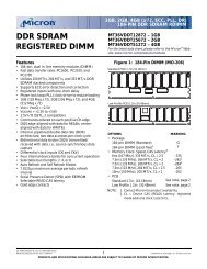
Functional Block Diagram<br />
Figure 1: 2 Meg x 32 S<strong>DRAM</strong><br />
CKE<br />
CLK<br />
CS#<br />
WE#<br />
CAS#<br />
RAS#<br />
A0–A10,<br />
BA0, BA1<br />
13<br />
COMMAND<br />
DECODE<br />
MODE REGISTER<br />
ADDRESS<br />
REGISTER<br />
CONTROL<br />
LOGIC<br />
11<br />
REFRESH<br />
COUNTER<br />
11<br />
8<br />
2<br />
11<br />
ROW-<br />
ADDRESS<br />
MUX<br />
2<br />
11<br />
BANK<br />
CONTROL<br />
LOGIC<br />
COLUMN-<br />
ADDRESS<br />
COUNTER/<br />
LATCH<br />
BANK 0<br />
ROW-<br />
ADDRESS<br />
LATCH<br />
&<br />
DECODER<br />
8<br />
2048<br />
BANK 3<br />
BANK 2<br />
BANK 1<br />
BANK 0<br />
BANK0<br />
MEMORY<br />
ARRAY<br />
(2,048 x 256 x 32)<br />
SENSE AMPLIFIERS<br />
64Mb: x32 S<strong>DRAM</strong><br />
Functional Block Diagram<br />
PDF: 09005aef811ce1fe/Source: 09005aef811ce1d5 <strong>Micron</strong> Technology, Inc., reserves the right to change products or specifications without notice.<br />
64MS<strong>DRAM</strong>x32_2.fm - Rev. J 12/08 EN 6 ©2001 <strong>Micron</strong> Technology, Inc. All rights reserved.<br />
8192<br />
I/O GATING<br />
DQM MASK LOGIC<br />
READ DATA LATCH<br />
WRITE DRIVERS<br />
256<br />
(x32)<br />
COLUMN<br />
DECODER<br />
32<br />
32<br />
4 4<br />
DATA<br />
OUTPUT<br />
REGISTER<br />
DATA<br />
INPUT<br />
REGISTER<br />
32<br />
DQM0–<br />
DQM3<br />
DQ0–<br />
DQ31
Pin/Ball Assignments and Descriptions<br />
Figure 2: 86-Pin TSOP (Top View)<br />
VDD<br />
DQ0<br />
VDDQ<br />
DQ1<br />
DQ2<br />
VSSQ<br />
DQ3<br />
DQ4<br />
VDDQ<br />
DQ5<br />
DQ6<br />
VSSQ<br />
DQ7<br />
NC<br />
VDD<br />
DQM0<br />
WE#<br />
CAS#<br />
RAS#<br />
CS#<br />
NC<br />
BA0<br />
BA1<br />
A10<br />
A0<br />
A1<br />
A2<br />
DQM2<br />
VDD<br />
NC<br />
DQ16<br />
VSSQ<br />
DQ17<br />
DQ18<br />
VDDQ<br />
DQ19<br />
DQ20<br />
VSSQ<br />
DQ21<br />
DQ22<br />
VDDQ<br />
DQ23<br />
VDD<br />
1<br />
2<br />
3<br />
4<br />
5<br />
6<br />
7<br />
8<br />
9<br />
10<br />
11<br />
12<br />
13<br />
14<br />
15<br />
16<br />
17<br />
18<br />
19<br />
20<br />
21<br />
22<br />
23<br />
24<br />
25<br />
26<br />
27<br />
28<br />
29<br />
30<br />
31<br />
32<br />
33<br />
34<br />
35<br />
36<br />
37<br />
38<br />
39<br />
40<br />
41<br />
42<br />
43<br />
Note: The # symbol indicates signal is active LOW.<br />
64Mb: x32 S<strong>DRAM</strong><br />
Pin/Ball Assignments and Descriptions<br />
PDF: 09005aef811ce1fe/Source: 09005aef811ce1d5 <strong>Micron</strong> Technology, Inc., reserves the right to change products or specifications without notice.<br />
64MS<strong>DRAM</strong>x32_2.fm - Rev. J 12/08 EN 7 ©2001 <strong>Micron</strong> Technology, Inc. All rights reserved.<br />
86<br />
85<br />
84<br />
83<br />
82<br />
81<br />
80<br />
79<br />
78<br />
77<br />
76<br />
75<br />
74<br />
73<br />
72<br />
71<br />
70<br />
69<br />
68<br />
67<br />
66<br />
65<br />
64<br />
63<br />
62<br />
61<br />
60<br />
59<br />
58<br />
57<br />
56<br />
55<br />
54<br />
53<br />
52<br />
51<br />
50<br />
49<br />
48<br />
47<br />
46<br />
45<br />
44<br />
VSS<br />
DQ15<br />
VSSQ<br />
DQ14<br />
DQ13<br />
VDDQ<br />
DQ12<br />
DQ11<br />
VSSQ<br />
DQ10<br />
DQ9<br />
VDDQ<br />
DQ8<br />
NC<br />
VSS<br />
DQM1<br />
NC<br />
NC<br />
CLK<br />
CKE<br />
A9<br />
A8<br />
A7<br />
A6<br />
A5<br />
A4<br />
A3<br />
DQM3<br />
VSS<br />
NC<br />
DQ31<br />
VDDQ<br />
DQ30<br />
DQ29<br />
VSSQ<br />
DQ28<br />
DQ27<br />
VDDQ<br />
DQ26<br />
DQ25<br />
VSSQ<br />
DQ24<br />
VSS
Figure 3: 90-Ball VFBGA (Top View, Ball Down)<br />
A<br />
B<br />
C<br />
D<br />
E<br />
F<br />
G<br />
H<br />
J<br />
K<br />
L<br />
M<br />
N<br />
P<br />
R<br />
1 2 3 4 5 6 7 8 9<br />
DQ26<br />
DQ28<br />
VSSQ<br />
VSSQ<br />
VDDQ<br />
VSS<br />
A4<br />
A7<br />
CLK<br />
DQM1<br />
VDDQ<br />
VSSQ<br />
VSSQ<br />
DQ11<br />
DQ13<br />
DQ24<br />
VDDQ<br />
DQ27<br />
DQ29<br />
DQ31<br />
DQM3<br />
A5<br />
A8<br />
CKE<br />
NC<br />
DQ8<br />
DQ10<br />
DQ12<br />
VDDQ<br />
DQ15<br />
VSS<br />
VSSQ<br />
DQ25<br />
DQ30<br />
NC<br />
A3<br />
A6<br />
NC<br />
A9<br />
NC<br />
VSS<br />
DQ9<br />
DQ14<br />
VSSQ<br />
VSS<br />
64Mb: x32 S<strong>DRAM</strong><br />
Pin/Ball Assignments and Descriptions<br />
PDF: 09005aef811ce1fe/Source: 09005aef811ce1d5 <strong>Micron</strong> Technology, Inc., reserves the right to change products or specifications without notice.<br />
64MS<strong>DRAM</strong>x32_2.fm - Rev. J 12/08 EN 8 ©2001 <strong>Micron</strong> Technology, Inc. All rights reserved.<br />
VDD<br />
VDDQ<br />
DQ22<br />
DQ17<br />
NC<br />
A2<br />
A10<br />
NC<br />
BA0<br />
CAS#<br />
VDD<br />
DQ6<br />
DQ1<br />
VDDQ<br />
VDD<br />
DQ23<br />
VSSQ<br />
DQ20<br />
DQ18<br />
DQ16<br />
DQM2<br />
A0<br />
BA1<br />
CS#<br />
WE#<br />
DQ7<br />
DQ5<br />
DQ3<br />
VSSQ<br />
DQ0<br />
DQ21<br />
DQ19<br />
VDDQ<br />
VDDQ<br />
VSSQ<br />
VDD<br />
A1<br />
NC<br />
RAS#<br />
DQM0<br />
VSSQ<br />
VDDQ<br />
VDDQ<br />
DQ4<br />
DQ2
Table 4: Pin/Ball Descriptions<br />
86-Pin TSOP<br />
Numbers<br />
64Mb: x32 S<strong>DRAM</strong><br />
Pin/Ball Assignments and Descriptions<br />
90-Ball VFBGA<br />
Numbers Symbol Type Description<br />
68 J1 CLK Input Clock: CLK is driven by the system clock. All S<strong>DRAM</strong> input signals<br />
are sampled on the positive edge of CLK. CLK also increments<br />
the internal burst counter and controls the output registers.<br />
67 J2 CKE Input Clock enable: CKE activates (HIGH) and deactivates (LOW) the<br />
CLK signal. Deactivating the clock provides PRECHARGE powerdown<br />
and SELF REFRESH operation (all banks idle), ACTIVE<br />
power-down (row active in any bank), or CLOCK SUSPEND<br />
operation (burst/access in progress). CKE is synchronous except<br />
after the device enters power-down and self refresh modes,<br />
where CKE becomes asynchronous until after exiting the same<br />
mode. The input buffers, including CLK, are disabled during<br />
power-down and self refresh modes, providing low standby<br />
power. CKE may be tied HIGH.<br />
20 J8 CS# Input Chip select: CS# enables (registered LOW) and disables<br />
(registered HIGH) the command decoder. All commands are<br />
masked when CS# is registered HIGH, but READ/WRITE bursts<br />
already in progress will continue and DQM operation will retain<br />
its DQ mask capability while CS# is HIGH. CS# provides for<br />
external bank selection on systems with multiple banks. CS# is<br />
considered part of the command code.<br />
17, 18, 19 K8, K7, J9 WE#,<br />
CAS#,<br />
RAS#<br />
16, 71, 28, 59 K9, K1, F8, F2 DQM0–<br />
DQM3<br />
Input Command inputs: WE#, CAS#, and RAS# (along with CS#)<br />
define the command being entered.<br />
Input Input/output mask: DQM is sampled HIGH and is an input<br />
mask signal for write accesses and an output enable signal for<br />
read accesses. Input data is masked during a WRITE cycle. The<br />
output buffers are placed in a High-Z state (2-clock latency)<br />
during a READ cycle. DQM0 corresponds to DQ0–DQ7; DQM1<br />
corresponds to DQ8–DQ15; DQM2 corresponds to DQ16–DQ23;<br />
and DQM3 corresponds to DQ24–DQ31. DQM0–DQM3 are<br />
considered same state when referenced as DQM.<br />
22, 23 J7, H8 BA0, BA1 Input Bank address input(s): BA0 and BA1 define to which bank the<br />
ACTIVE, READ, WRITE, or PRECHARGE command is being<br />
applied.<br />
25–27, 60–66,<br />
24<br />
2, 4, 5, 7, 8, 10,<br />
11, 13, 74, 76,<br />
77, 79, 80, 82,<br />
83, 85, 31, 33,<br />
34, 36, 37, 39,<br />
40, 42, 45, 47,<br />
48, 50, 51, 53,<br />
54, 56<br />
G8, G9, F7, F3,<br />
G1, G2, G3, H1,<br />
H2, J3, G7<br />
R8, N7, R9, N8,<br />
P9, M8, M7, L8,<br />
L2, M3, M2, P1,<br />
N2, R1, N3, R2,<br />
E8, D7, D8, B9,<br />
C8, A9, C7, A8,<br />
A2, C3, A1, C2,<br />
B1, D2, D3, E2<br />
A0–A10 Input Address inputs: A0–A10 are sampled during the ACTIVE<br />
command (row-address A0–A10) and READ/WRITE command<br />
(column-address A0–A7 with A10 defining auto precharge) to<br />
select one location out of the memory array in the respective<br />
bank. A10 is sampled during a PRECHARGE command to<br />
determine whether all banks are to be precharged (A10 HIGH)<br />
or bank selected by BA0, BA1 (LOW). The address inputs also<br />
provide the op-code during a LOAD MODE REGISTER command.<br />
DQ0–<br />
DQ31<br />
Input/<br />
Output<br />
Data I/Os: Data bus.<br />
PDF: 09005aef811ce1fe/Source: 09005aef811ce1d5 <strong>Micron</strong> Technology, Inc., reserves the right to change products or specifications without notice.<br />
64MS<strong>DRAM</strong>x32_2.fm - Rev. J 12/08 EN 9 ©2001 <strong>Micron</strong> Technology, Inc. All rights reserved.
Table 4: Pin/Ball Descriptions (continued)<br />
86-Pin TSOP<br />
Numbers<br />
3, 9, 35, 41, 49,<br />
55, 75, 81<br />
6, 12, 32, 38,<br />
46, 52, 78, 84<br />
Functional Description<br />
Initialization<br />
90-Ball VFBGA<br />
Numbers Symbol Type Description<br />
B2, B7, C9, D9,<br />
E1, L1, M9, N9,<br />
P2, P7<br />
B8, B3, C1, D1,<br />
E9, L9, M1, N1,<br />
P3, P8<br />
64Mb: x32 S<strong>DRAM</strong><br />
Functional Description<br />
VDDQ Supply DQ power supply: Isolated on the die for improved noise<br />
immunity.<br />
VSSQ Supply DQ ground: Provide isolated ground to DQs for improved noise<br />
immunity.<br />
1, 15, 29, 43 A7, F9, L7, R7 VDD Supply Power supply: +3.3V ±0.3V. (See note 27 on page 50.)<br />
44, 58, 72, 86 A3, F1, L3, R3 VSS Supply Ground.<br />
14, 21, 30, 57, E3, E7, H3, H7, NC – No connect: These pins/balls should be left unconnected. Pin 70<br />
69, 70, 73 K2, K3, H9<br />
is reserved for SSTL reference voltage supply. H7 is a no connect<br />
for this part but may be used as A12 in future designs. H9 is used<br />
as A11 in 128Mb, 256Mb, and 512Mb x32 FBGAs. PCB designs<br />
that accommodate different densities must account for A11 with<br />
stuffing options.<br />
In general, this 64Mb S<strong>DRAM</strong> (512K x 32 x 4 banks) is a 4-bank <strong>DRAM</strong> that operates at<br />
3.3V and includes a synchronous interface (all signals are registered on the positive edge<br />
of the clock signal, CLK). Each of the 16,777,216-bit banks is organized as 2,048 rows by<br />
256 columns by 32 bits.<br />
Read and write accesses to the S<strong>DRAM</strong> are burst oriented; accesses start at a selected<br />
location and continue for a programmed number of locations in a programmed<br />
sequence. Accesses begin with the registration of an ACTIVE command, which is then<br />
followed by a READ or WRITE command. The address bits registered coincident with the<br />
ACTIVE command are used to select the bank and row to be accessed (BA0 and BA1<br />
select the bank, A0–A10 select the row). The address bits (A0–A7) registered coincident<br />
with the READ or WRITE command are used to select the starting column location for<br />
the burst access.<br />
Prior to normal operation, the S<strong>DRAM</strong> must be initialized. The following sections<br />
provide detailed information covering device initialization, register definition,<br />
command descriptions, and device operation.<br />
S<strong>DRAM</strong>s must be powered up and initialized in a predefined manner. Operational<br />
procedures other than those specified may result in undefined operation. After power is<br />
applied to VDD and VDDQ (simultaneously) and the clock is stable (stable clock is<br />
defined as a signal cycling within timing constraints specified for the clock pin), the<br />
S<strong>DRAM</strong> requires a 100µs delay prior to issuing any command other than a COMMAND<br />
INHIBIT or NOP. Starting at some point during this 100µs period, and continuing at least<br />
through the end of this period, COMMAND INHIBIT or NOP commands must be<br />
applied.<br />
When the 100µs delay has been satisfied with at least one COMMAND INHIBIT or NOP<br />
command having been applied, a PRECHARGE command should be applied. All banks<br />
must then be precharged, thereby placing the device in the all banks idle state.<br />
PDF: 09005aef811ce1fe/Source: 09005aef811ce1d5 <strong>Micron</strong> Technology, Inc., reserves the right to change products or specifications without notice.<br />
64MS<strong>DRAM</strong>x32_2.fm - Rev. J 12/08 EN 10 ©2001 <strong>Micron</strong> Technology, Inc. All rights reserved.
64Mb: x32 S<strong>DRAM</strong><br />
Functional Description<br />
When in the idle state, at least two AUTO REFRESH cycles must be performed. After the<br />
AUTO REFRESH cycles are complete, the S<strong>DRAM</strong> is ready for mode register programming.<br />
Because the mode register will power up in an unknown state, it must be loaded<br />
prior to applying any operational command. If desired, the two AUTO REFRESH<br />
commands can be issued after the LOAD MODE REGISTER command.<br />
The recommended power-up sequence for S<strong>DRAM</strong>s:<br />
1. Simultaneously apply power to VDD and VDDQ.<br />
2. Assert and hold CKE at a LVTTL logic LOW since all inputs and outputs are LVTTLcompatible.<br />
3. Provide stable CLOCK signal. Stable clock is defined as a signal cycling within timing<br />
constraints specified for the clock pin.<br />
4. Wait at least 100µs prior to issuing any command other than a COMMAND INHIBIT<br />
or NOP.<br />
5. Starting at some point during this 100µs period, bring CKE HIGH. Continuing at least<br />
through the end of this period, 1 or more COMMAND INHIBIT or NOP commands<br />
must be applied.<br />
6. Perform a PRECHARGE ALL command.<br />
7. Wait at least t RP time; during this time,0 NOPs or DESELECT commands must be<br />
given. All banks will complete their precharge, thereby placing the device in the all<br />
banks idle state.<br />
8. Issue an AUTO REFRESH command.<br />
9. Wait at least t RFC time, during which only NOPs or COMMAND INHIBIT commands<br />
are allowed.<br />
10. Issue an AUTO REFRESH command.<br />
11. Wait at least t RFC time, during which only NOPs or COMMAND INHIBIT commands<br />
are allowed.<br />
12. The S<strong>DRAM</strong> is now ready for mode register programming. Because the mode register<br />
will power up in an unknown state, it should be loaded with desired bit values prior to<br />
applying any operational command. Using the LMR command, program the mode<br />
register. The mode register is programmed via the MODE REGISTER SET command<br />
with BA1 = 0, BA0 = 0 and retains the stored information until it is programmed again<br />
or the device loses power. Not programming the mode register upon initialization will<br />
result in default settings which may not be desired. Outputs are guaranteed High-Z<br />
after the LMR command is issued. Outputs should be High-Z already before the LMR<br />
command is issued.<br />
13. Wait at least tMRD time, during which only NOP or DESELECT commands are<br />
allowed.<br />
At this point the <strong>DRAM</strong> is ready for any valid command.<br />
Note: If desired, more than two AUTO REFRESH commands can be issued in the sequence.<br />
After steps 9 and 10 are complete, repeat them until the desired number of AUTO<br />
REFRESH + t RFC loops is achieved.<br />
PDF: 09005aef811ce1fe/Source: 09005aef811ce1d5 <strong>Micron</strong> Technology, Inc., reserves the right to change products or specifications without notice.<br />
64MS<strong>DRAM</strong>x32_2.fm - Rev. J 12/08 EN 11 ©2001 <strong>Micron</strong> Technology, Inc. All rights reserved.
Register Definition<br />
Mode Register<br />
Burst Length<br />
64Mb: x32 S<strong>DRAM</strong><br />
Functional Description<br />
The mode register is used to define the specific mode of operation of the S<strong>DRAM</strong>. This<br />
definition includes the selection of a burst length, a burst type, a CL, an operating mode<br />
and a write burst mode, as shown in Figure 4 on page 13. The mode register is<br />
programmed via the LOAD MODE REGISTER command and will retain the stored information<br />
until it is programmed again or the device loses power.<br />
Mode register bits M0–M2 specify the burst length, M3 specifies the type of burst<br />
(sequential or interleaved), M4–M6 specify the CL, M7, and M8 specify the operating<br />
mode, M9 specifies the write burst mode, and M10 is reserved for future use.<br />
The mode register must be loaded when all banks are idle, and the controller must wait<br />
the specified time before initiating the subsequent operation. Violating either of these<br />
requirements will result in unspecified operation.<br />
Read and write accesses to the S<strong>DRAM</strong> are burst oriented, with the burst length being<br />
programmable, as shown in Figure 4. The burst length determines the maximum<br />
number of column locations that can be accessed for a given READ or WRITE command.<br />
Burst lengths of 1, 2, 4, or 8 locations are available for both the sequential and the interleaved<br />
burst types, and a full-page burst is available for the sequential type. The fullpage<br />
burst is used in conjunction with the BURST TERMINATE command to generate<br />
arbitrary burst lengths.<br />
Reserved states should not be used, as unknown operation or incompatibility with<br />
future versions may result.<br />
When a READ or WRITE command is issued, a block of columns equal to the burst<br />
length is effectively selected. All accesses for that burst take place within this block,<br />
meaning that the burst will wrap within the block if a boundary is reached. The block is<br />
uniquely selected by A1–A7 when BL = 2; by A2–A7 when BL = 4; and by A3–A7 when the<br />
BL = 8. The remaining (least significant) address bit(s) is (are) used to select the starting<br />
location within the block. Full-page bursts wrap within the page if the boundary is<br />
reached.<br />
PDF: 09005aef811ce1fe/Source: 09005aef811ce1d5 <strong>Micron</strong> Technology, Inc., reserves the right to change products or specifications without notice.<br />
64MS<strong>DRAM</strong>x32_2.fm - Rev. J 12/08 EN 12 ©2001 <strong>Micron</strong> Technology, Inc. All rights reserved.
Figure 4: Mode Register Definition<br />
Burst Type<br />
M9<br />
0<br />
0<br />
–<br />
1<br />
M8 M7<br />
0<br />
–<br />
M6–M0<br />
Defined<br />
–<br />
A10<br />
10<br />
Reserved WB<br />
Program<br />
A10, BA0, and BA1 = “0”<br />
to ensure compatibility<br />
with future devices.<br />
Write Burst Mode<br />
Programmed Burst Length<br />
Single Location Access<br />
Operating Mode<br />
Standard Operation<br />
All other states reserved<br />
A9 A8 A7 A6 A5 A4 A3 A2 A1 A0<br />
9 8 7 6 5 4 3 2 1 0<br />
M6 M5 M4<br />
0<br />
0<br />
0<br />
0<br />
1<br />
1<br />
1<br />
1<br />
Op Mode<br />
0<br />
0<br />
1<br />
1<br />
0<br />
0<br />
1<br />
1<br />
0<br />
1<br />
0<br />
1<br />
0<br />
1<br />
0<br />
1<br />
CAS Latency BT<br />
64Mb: x32 S<strong>DRAM</strong><br />
Functional Description<br />
Accesses within a given burst may be programmed to be either sequential or interleaved;<br />
this is referred to as the burst type and is selected via bit M3.<br />
The ordering of accesses within a burst is determined by the burst length, the burst type,<br />
and the starting column address, as shown in Table 5 on page 14.<br />
PDF: 09005aef811ce1fe/Source: 09005aef811ce1d5 <strong>Micron</strong> Technology, Inc., reserves the right to change products or specifications without notice.<br />
64MS<strong>DRAM</strong>x32_2.fm - Rev. J 12/08 EN 13 ©2001 <strong>Micron</strong> Technology, Inc. All rights reserved.<br />
M3<br />
0<br />
1<br />
CAS Latency<br />
Reserved<br />
1<br />
2<br />
3<br />
Reserved<br />
Reserved<br />
Reserved<br />
Reserved<br />
Burst Length<br />
M2 M1 M0<br />
0<br />
0<br />
0<br />
0<br />
1<br />
1<br />
1<br />
1<br />
0<br />
0<br />
1<br />
1<br />
0<br />
0<br />
1<br />
1<br />
0<br />
1<br />
0<br />
1<br />
0<br />
1<br />
0<br />
1<br />
M3 = 0<br />
1<br />
2<br />
4<br />
8<br />
Reserved<br />
Reserved<br />
Reserved<br />
Full Page<br />
Address Bus<br />
Mode Register (Mx)<br />
Burst Length<br />
Burst Type<br />
Sequential<br />
Interleaved<br />
M3 = 1<br />
1<br />
2<br />
4<br />
8<br />
Reserved<br />
Reserved<br />
Reserved<br />
Reserved
Table 5: Burst Definition<br />
CAS Latency<br />
64Mb: x32 S<strong>DRAM</strong><br />
Functional Description<br />
Burst<br />
Order of Accesses Within a Burst<br />
Length Starting Column Address Type = Sequential Type = Interleaved<br />
2 A0<br />
0 0-1 0-1<br />
1 1-0 1-0<br />
4 A1 A0<br />
0 0 0-1-2-3 0-1-2-3<br />
0 1 1-2-3-0 1-0-3-2<br />
1 0 2-3-0-1 2-3-0-1<br />
1 1 3-0-1-2 3-2-1-0<br />
8 A2 A1 A0<br />
0 0 0 0-1-2-3-4-5-6-7 0-1-2-3-4-5-6-7<br />
0 0 1 1-2-3-4-5-6-7-0 1-0-3-2-5-4-7-6<br />
0 1 0 2-3-4-5-6-7-0-1 2-3-0-1-6-7-4-5<br />
0 1 1 3-4-5-6-7-0-1-2 3-2-1-0-7-6-5-4<br />
1 0 0 4-5-6-7-0-1-2-3 4-5-6-7-0-1-2-3<br />
1 0 1 5-6-7-0-1-2-3-4 5-4-7-6-1-0-3-2<br />
1 1 0 6-7-0-1-2-3-4-5 6-7-4-5-2-3-0-1<br />
1 1 1 7-0-1-2-3-4-5-6 7-6-5-4-3-2-1-0<br />
Full page<br />
(256)<br />
n = A0–A10<br />
(location 0–256)<br />
Cn, Cn + 1, Cn + 2,<br />
Cn + 3, Cn + 4...<br />
…Cn - 1, Cn…<br />
Not supported<br />
Notes: 1. For BL = 2, A1–A7 select the block-of-two burst; A0 selects the starting column within the<br />
block.<br />
2. For BL = 4, A2–A7 select the block-of-four burst; A0–A1 select the starting column within<br />
the block.<br />
3. For BL = 8, A3–A7 select the block-of-eight burst; A0–A2 select the starting column within<br />
the block.<br />
4. For a full-page burst, the full row is selected and A0–A7 select the starting column.<br />
5. Whenever a boundary of the block is reached within a given sequence above, the following<br />
access wraps within the block.<br />
6. For BL = 1, A0–A7 select the unique column to be accessed, and mode register bit M3 is<br />
ignored.<br />
The CAS latency is the delay, in clock cycles, between the registration of a READ<br />
command and the availability of the first piece of output data. The latency can be set to<br />
1, 2, or 3 clocks.<br />
If a READ command is registered at clock edge n, and the latency is m clocks, the data<br />
will be available by clock edge n + m. The DQs will start driving as a result of the clock<br />
edge one cycle earlier (n + m - 1), and provided that the relevant access times are met,<br />
the data will be valid by clock edge n + m. For example, assuming that the clock cycle<br />
time is such that all relevant access times are met, if a READ command is registered at T0<br />
and the latency is programmed to 2 clocks, the DQs will start driving after T1 and the<br />
data will be valid by T2, as shown in Figure 5 on page 15. Table 6 on page 15 indicates the<br />
operating frequencies at which each CAS latency setting can be used.<br />
Reserved states should not be used because unknown operation or incompatibility with<br />
future versions may result.<br />
PDF: 09005aef811ce1fe/Source: 09005aef811ce1d5 <strong>Micron</strong> Technology, Inc., reserves the right to change products or specifications without notice.<br />
64MS<strong>DRAM</strong>x32_2.fm - Rev. J 12/08 EN 14 ©2001 <strong>Micron</strong> Technology, Inc. All rights reserved.
Figure 5: CAS Latency<br />
Table 6: CAS Latency<br />
CLK<br />
DQ<br />
CLK<br />
DQ<br />
T0<br />
T0<br />
COMMAND READ<br />
NOP<br />
T1 T2<br />
T3<br />
Allowable Operating Frequency (MHz)<br />
64Mb: x32 S<strong>DRAM</strong><br />
Functional Description<br />
Speed<br />
CL = 1 CL = 2 CL = 3<br />
-5 – – ≤ 200<br />
-55 – – ≤ 183<br />
-6 ≤ 50 ≤ 100 ≤ 166<br />
-7 ≤ 50 ≤ 100 ≤ 143<br />
T1<br />
COMMAND READ<br />
NOP<br />
CLK<br />
DQ<br />
T0<br />
tLZ<br />
t AC<br />
CL = 1<br />
COMMAND READ<br />
NOP<br />
PDF: 09005aef811ce1fe/Source: 09005aef811ce1d5 <strong>Micron</strong> Technology, Inc., reserves the right to change products or specifications without notice.<br />
64MS<strong>DRAM</strong>x32_2.fm - Rev. J 12/08 EN 15 ©2001 <strong>Micron</strong> Technology, Inc. All rights reserved.<br />
t OH<br />
DOUT<br />
CL = 3<br />
T2<br />
T1 T2<br />
T3<br />
tLZ<br />
tAC<br />
CL = 2<br />
NOP<br />
NOP<br />
t OH<br />
DOUT<br />
tLZ<br />
tAC<br />
NOP<br />
t OH<br />
DOUT<br />
T4<br />
DON’T CARE<br />
UNDEFINED
Operating Mode<br />
Write Burst Mode<br />
Commands<br />
64Mb: x32 S<strong>DRAM</strong><br />
Commands<br />
The normal operating mode is selected by setting M7 and M8 to zero; other combinations<br />
of values for M7 and M8 are reserved for future use and/or test modes. The<br />
programmed burst length applies to both read and write bursts.<br />
Test modes and reserved states should not be used because unknown operation or<br />
incompatibility with future versions may result.<br />
When M9 = 0, the burst length programmed via M0–M2 applies to both read and write<br />
bursts; when M9 = 1, the programmed burst length applies to read bursts, but write<br />
accesses are single-location (nonburst) accesses.<br />
Truth Table 1 provides a quick reference of available commands. This is followed by a<br />
written description of each command. Three additional Truth Tables appear following<br />
“Operations” on page 19; these tables provide current state/next state information.<br />
Table 7: Truth Table 1 – Commands and DQM Operation<br />
CKE is HIGH for all commands shown except SELF REFRESH<br />
Name (Function) CS# RAS# CAS# WE# DQM ADDR DQs Notes<br />
COMMAND INHIBIT (NOP) H X X X X X X<br />
NO OPERATION (NOP) L H H H X X X<br />
ACTIVE (Select bank and activate row) L L H H X Bank/row X 1<br />
READ (Select bank and column, and start READ<br />
burst)<br />
L H L H L/H7 Bank/col X 2<br />
WRITE (Select bank and column, and start WRITE<br />
burst)<br />
L H L L L/H7 Bank/col Valid 2<br />
BURST TERMINATE L H H L X X Active<br />
PRECHARGE (Deactivate row in bank or banks) L L H L X Code X 3<br />
AUTO REFRESH or SELF REFRESH (Enter self refresh<br />
mode)<br />
L L L H X X X 4, 5<br />
LOAD MODE REGISTER L L L L X Op-code X 6<br />
WRITE ENABLE/OUTPUT ENABLE – – – – L – Active 7<br />
WRITE INHIBIT/OUTPUT HIGH-Z – – – – H – High-Z 7<br />
Notes: 1. A0–A10 provide row address, BA0 and BA1 determine which bank is made active.<br />
2. A0–A7 provide column address; A10 HIGH enables the auto precharge feature (nonpersistent),<br />
while A10 LOW disables the auto precharge feature; BA0 and BA1 determine which<br />
bank is being read from or written to.<br />
3. A10 LOW: BA0 and BA1 determine the bank being precharged. A10 HIGH: all banks precharged<br />
and BA0 and BA1 are “Don’t Care.”<br />
4. This command is AUTO REFRESH if CKE is HIGH; SELF REFRESH if CKE is LOW.<br />
5. Internal refresh counter controls row addressing; all inputs and I/Os are “Don’t Care” except<br />
for CKE.<br />
6. A0–A10 define the op-code written to the mode register.<br />
7. Activates or deactivates the DQs during WRITEs (zero-clock delay) and READs (two-clock<br />
delay). DQM0 controls DQ0–DQ7; DQM1 controls DQ8–DQ15; DQM2 controls DQ16–DQ23;<br />
and DQM3 controls DQ24–DQ31.<br />
PDF: 09005aef811ce1fe/Source: 09005aef811ce1d5 <strong>Micron</strong> Technology, Inc., reserves the right to change products or specifications without notice.<br />
64MS<strong>DRAM</strong>x32_2.fm - Rev. J 12/08 EN 16 ©2001 <strong>Micron</strong> Technology, Inc. All rights reserved.
COMMAND INHIBIT<br />
NO OPERATION (NOP)<br />
LOAD MODE REGISTER<br />
ACTIVE<br />
READ<br />
WRITE<br />
64Mb: x32 S<strong>DRAM</strong><br />
Commands<br />
The COMMAND INHIBIT function prevents new commands from being executed by the<br />
S<strong>DRAM</strong>, regardless of whether the CLK signal is enabled. The S<strong>DRAM</strong> is effectively deselected.<br />
Operations already in progress are not affected.<br />
The NO OPERATION (NOP) command is used to perform an NOP to an S<strong>DRAM</strong> that is<br />
selected (CS# is LOW). This prevents unwanted commands from being registered during<br />
idle or wait states. Operations already in progress are not affected.<br />
The mode register is loaded via inputs A0–A10. See “Mode Register” on page 12. The<br />
LOAD MODE REGISTER command can only be issued when all banks are idle, and a<br />
subsequent executable command cannot be issued until t MRD is met.<br />
The ACTIVE command is used to open (or activate) a row in a particular bank for a<br />
subsequent access. The value on the BA0, BA1 inputs selects the bank, and the address<br />
provided on inputs A0–A10 selects the row. This row remains active (or open) for<br />
accesses until a PRECHARGE command is issued to that bank. A PRECHARGE<br />
command must be issued before opening a different row in the same bank.<br />
The READ command is used to initiate a burst read access to an active row. The value on<br />
the BA0 and BA1 (B1) inputs selects the bank, and the address provided on inputs A0–A7<br />
selects the starting column location. The value on input A10 determines whether auto<br />
precharge is used. If auto precharge is selected, the row being accessed will be<br />
precharged at the end of the read burst; if auto precharge is not selected, the row will<br />
remain open for subsequent accesses. Read data appears on the DQs subject to the logic<br />
level on the DQM inputs two clocks earlier. If a given DQMx signal was registered HIGH,<br />
the corresponding DQs will be High-Z two clocks later; if the DQMx signal was registered<br />
LOW, the corresponding DQs will provide valid data. DQM0 corresponds to DQ0–DQ7,<br />
DQM1 corresponds to DQ8–DQ15, DQM2 corresponds to DQ16–DQ23, and DQM3<br />
corresponds to DQ24–DQ31.<br />
The WRITE command is used to initiate a burst write access to an active row. The value<br />
on the BA0 and BA1 inputs selects the bank, and the address provided on inputs A0–A7<br />
selects the starting column location. The value on input A10 determines whether or not<br />
auto precharge is used. If auto precharge is selected, the row being accessed will be<br />
precharged at the end of the write burst; if auto precharge is not selected, the row will<br />
remain open for subsequent accesses. Input data appearing on the DQs is written to the<br />
memory array subject to the DQM input logic level appearing coincident with the data.<br />
If a given DQM signal is registered LOW, the corresponding data will be written to<br />
memory; if the DQM signal is registered HIGH, the corresponding data inputs will be<br />
ignored, and a write will not be executed to that byte/column location.<br />
PDF: 09005aef811ce1fe/Source: 09005aef811ce1d5 <strong>Micron</strong> Technology, Inc., reserves the right to change products or specifications without notice.<br />
64MS<strong>DRAM</strong>x32_2.fm - Rev. J 12/08 EN 17 ©2001 <strong>Micron</strong> Technology, Inc. All rights reserved.
PRECHARGE<br />
Auto Precharge<br />
BURST TERMINATE<br />
AUTO REFRESH<br />
SELF REFRESH<br />
64Mb: x32 S<strong>DRAM</strong><br />
Commands<br />
The PRECHARGE command is used to deactivate the open row in a particular bank or<br />
the open row in all banks. The bank(s) will be available for a subsequent row access a<br />
specified time ( t RP) after the PRECHARGE command is issued. Input A10 determines<br />
whether one or all banks are to be precharged, and in the case where only one bank is to<br />
be precharged, inputs BA0 and BA1 select the bank. Otherwise BA0 and BA1 are treated<br />
as “Don’t Care.” After a bank has been precharged, it is in the idle state and must be activated<br />
prior to any READ or WRITE commands being issued to that bank.<br />
Auto precharge is a feature that performs the same individual-bank precharge function<br />
described above, without requiring an explicit command. This is accomplished by using<br />
A10 to enable auto precharge in conjunction with a specific READ or WRITE command.<br />
A precharge of the bank/row that is addressed with the READ or WRITE command is<br />
automatically performed upon completion of the READ or WRITE burst, except in the<br />
full-page burst mode, where AUTO PRECHARGE does not apply. Auto precharge is<br />
nonpersistent in that it is either enabled or disabled for each READ or WRITE command.<br />
Auto precharge ensures that the precharge is initiated at the earliest valid stage within a<br />
burst. The user must not issue another command to the same bank until the precharge<br />
time ( t RP) is completed. This is determined as if an explicit PRECHARGE command was<br />
issued at the earliest possible time, as described for each burst type in “Operations” on<br />
page 19.<br />
The BURST TERMINATE command is used to truncate either fixed-length or full-page<br />
bursts. The most recently registered READ or WRITE command prior to the BURST<br />
TERMINATE command will be truncated, as shown in “Operations” on page 19. The<br />
BURST TERMINATE command does not precharge the row; the row will remain open<br />
until a PRECHARGE command is issued.<br />
AUTO REFRESH is used during normal operation of the S<strong>DRAM</strong> and is analogous to<br />
CAS#-BEFORE-RAS# (CBR) refresh in conventional <strong>DRAM</strong>s. This command is nonpersistent,<br />
so it must be issued each time a refresh is required.<br />
The addressing is generated by the internal refresh controller. This makes the address<br />
bits “Don’t Care” during an AUTO REFRESH command. Regardless of device width, the<br />
64Mb S<strong>DRAM</strong> requires 4,096 AUTO REFRESH cycles every 64ms (commercial and industrial)<br />
or 16ms (automotive). Providing a distributed AUTO REFRESH command every<br />
15.625µs (commercial and industrial) or 3.906µs (automotive) will meet the refresh<br />
requirement and ensure that each row is refreshed. Alternatively, 4,096 AUTO REFRESH<br />
commands can be issued in a burst at the minimum cycle rate ( t RFC), once every 64ms<br />
(commercial and industrial) or 16ms (automotive).<br />
The SELF REFRESH command can be used to retain data in the S<strong>DRAM</strong>, even if the rest<br />
of the system is powered down. When in the self refresh mode, the S<strong>DRAM</strong> retains data<br />
without external clocking. The SELF REFRESH command is initiated like an AUTO<br />
PDF: 09005aef811ce1fe/Source: 09005aef811ce1d5 <strong>Micron</strong> Technology, Inc., reserves the right to change products or specifications without notice.<br />
64MS<strong>DRAM</strong>x32_2.fm - Rev. J 12/08 EN 18 ©2001 <strong>Micron</strong> Technology, Inc. All rights reserved.
Operations<br />
Bank/Row Activation<br />
64Mb: x32 S<strong>DRAM</strong><br />
Commands<br />
REFRESH command except CKE is disabled (LOW). When the SELF REFRESH command<br />
is registered, all the inputs to the S<strong>DRAM</strong> become “Don’t Care” with the exception of<br />
CKE, which must remain LOW.<br />
After self refresh mode is engaged, the S<strong>DRAM</strong> provides its own internal clocking,<br />
causing it to perform its own AUTO REFRESH cycles. The S<strong>DRAM</strong> must remain in self<br />
refresh mode for a minimum period equal to t RAS and may remain in self refresh mode<br />
for an indefinite period beyond that.<br />
The procedure for exiting self refresh requires a sequence of commands. First, CLK must<br />
be stable (stable clock is defined as a signal cycling within timing constraints specified<br />
for the clock pin) prior to CKE going back HIGH. After CKE is HIGH, the S<strong>DRAM</strong> must<br />
have NOP commands issued (a minimum of two clocks) for t XSR because time is<br />
required for the completion of any internal refresh in progress.<br />
Upon exiting self refresh mode, AUTO REFRESH commands must be issued every<br />
15.625µs or less as both SELF REFRESH and AUTO REFRESH utilize the row refresh<br />
counter.<br />
Self refresh is not supported on automotive temperature devices.<br />
Before any READ or WRITE commands can be issued to a bank within the S<strong>DRAM</strong>, a row<br />
in that bank must be “opened.” This is accomplished via the ACTIVE command, which<br />
selects both the bank and the row to be activated. See Figure 6 on page 20.<br />
After opening a row (issuing an ACTIVE command), a READ or WRITE command may be<br />
issued to that row, subject to the tRCD specification. tRCD (MIN) should be divided by<br />
the clock period and rounded up to the next whole number to determine the earliest<br />
clock edge after the ACTIVE command on which a READ or WRITE command can be<br />
issued. For example, a tRCD specification of 20ns with a 125 MHz clock (8ns period)<br />
results in 2.5 clocks, rounded to 3. This is reflected in Figure 7 on page 20, which covers<br />
any case where 2 < tRCD (MIN)/ tCK - 3 (the same procedure is used to convert other<br />
specification limits from time units to clock cycles).<br />
A subsequent ACTIVE command to a different row in the same bank can only be issued<br />
after the previous active row has been “closed” (precharged). The minimum time<br />
interval between successive ACTIVE commands to the same bank is defined by t RC.<br />
A subsequent ACTIVE command to another bank can be issued while the first bank is<br />
being accessed, which results in a reduction of total row-access overhead. The minimum<br />
time interval between successive ACTIVE commands to different banks is defined by<br />
t RRD.<br />
PDF: 09005aef811ce1fe/Source: 09005aef811ce1d5 <strong>Micron</strong> Technology, Inc., reserves the right to change products or specifications without notice.<br />
64MS<strong>DRAM</strong>x32_2.fm - Rev. J 12/08 EN 19 ©2001 <strong>Micron</strong> Technology, Inc. All rights reserved.
Figure 6: Activating a Specific Row in a Specific Bank<br />
Figure 7: Example: Meeting t RCD (MIN) when 2 < t RCD (MIN)/ t CK - 3<br />
READs<br />
CLK<br />
CKE<br />
CS#<br />
RAS#<br />
CAS#<br />
WE#<br />
A0–A10<br />
BA0, BA1<br />
CLK<br />
HIGH<br />
T0<br />
COMMAND ACTIVE<br />
NOP<br />
ROW<br />
ADDRESS<br />
BANK<br />
ADDRESS<br />
DON´T CARE<br />
T1 T2<br />
T3<br />
t CK t CK t CK<br />
tRCD<br />
(MIN)<br />
tRCD (MIN) +0.5 tCK Notes: 1. tRCD (MIN) = 20ns, tCK = 8ns.<br />
2.<br />
t t<br />
RCD (MIN) x CK where x = number of clocks for equation to be true.<br />
64Mb: x32 S<strong>DRAM</strong><br />
Commands<br />
READ bursts are initiated with a READ command, as shown in Figure 8 on page 21.<br />
The starting column and bank addresses are provided with the READ command, and<br />
auto precharge either is enabled or disabled for that burst access. If auto precharge is<br />
enabled, the row being accessed is precharged at the completion of the burst. For the<br />
generic READ commands used in the following illustrations, auto precharge is disabled.<br />
During READ bursts, the valid data-out element from the starting column address will<br />
be available following the CAS latency after the READ command. Each subsequent dataout<br />
element will be valid by the next positive clock edge. Figure 9 on page 22 shows<br />
general timing for each possible CAS latency setting.<br />
PDF: 09005aef811ce1fe/Source: 09005aef811ce1d5 <strong>Micron</strong> Technology, Inc., reserves the right to change products or specifications without notice.<br />
64MS<strong>DRAM</strong>x32_2.fm - Rev. J 12/08 EN 20 ©2001 <strong>Micron</strong> Technology, Inc. All rights reserved.<br />
NOP<br />
READ or<br />
WRITE<br />
DON’T CARE
Figure 8: READ Command<br />
64Mb: x32 S<strong>DRAM</strong><br />
Commands<br />
Upon completion of a burst, assuming no other commands have been initiated, the DQs<br />
will go High-Z. A full-page burst will continue until terminated. (At the end of the page, it<br />
will wrap to column 0 and continue.)<br />
Data from any READ burst may be truncated with a subsequent READ command, and<br />
data from a fixed-length READ burst may be immediately followed by data from a READ<br />
command. In either case, a continuous flow of data can be maintained. The first data<br />
element from the new burst either follows the last element of a completed burst or the<br />
last desired data element of a longer burst that is being truncated. The new READ<br />
command should be issued x cycles before the clock edge at which the last desired data<br />
element is valid, where x equals CL - 1. This is shown in Figure 10 on page 23 for CL = 1,<br />
CL = 2, and CL = 3; data element n + 3 is either the last of a burst of four or the last desired<br />
of a longer burst. This 64Mb S<strong>DRAM</strong> uses a pipelined architecture and therefore does<br />
not require the 2n rule associated with a prefetch architecture. A READ command can be<br />
initiated on any clock cycle following a previous READ command. Full-speed random<br />
read accesses can be performed to the same bank, as shown in Figure 11 on page 24, or<br />
each subsequent READ may be performed to a different bank.<br />
CLK<br />
CKE<br />
CS#<br />
RAS#<br />
CAS#<br />
WE#<br />
A0–A7<br />
A8, A9<br />
A10<br />
BA0, 1<br />
HIGH<br />
COLUMN<br />
ADDRESS<br />
ENABLE AUTO PRECHARGE<br />
DISABLE AUTO PRECHARGE<br />
BANK<br />
ADDRESS<br />
DON’T CARE<br />
PDF: 09005aef811ce1fe/Source: 09005aef811ce1d5 <strong>Micron</strong> Technology, Inc., reserves the right to change products or specifications without notice.<br />
64MS<strong>DRAM</strong>x32_2.fm - Rev. J 12/08 EN 21 ©2001 <strong>Micron</strong> Technology, Inc. All rights reserved.
Figure 9: CAS Latency<br />
CLK<br />
DQ<br />
CLK<br />
DQ<br />
T0<br />
T0<br />
T1<br />
COMMAND READ<br />
NOP<br />
CLK<br />
DQ<br />
T0<br />
tLZ<br />
t AC<br />
CL = 1<br />
COMMAND READ<br />
NOP<br />
COMMAND READ<br />
NOP<br />
T1 T2<br />
T3<br />
64Mb: x32 S<strong>DRAM</strong><br />
Commands<br />
PDF: 09005aef811ce1fe/Source: 09005aef811ce1d5 <strong>Micron</strong> Technology, Inc., reserves the right to change products or specifications without notice.<br />
64MS<strong>DRAM</strong>x32_2.fm - Rev. J 12/08 EN 22 ©2001 <strong>Micron</strong> Technology, Inc. All rights reserved.<br />
t OH<br />
DOUT<br />
CL = 3<br />
T2<br />
T1 T2<br />
T3<br />
tLZ<br />
tAC<br />
CL = 2<br />
NOP<br />
NOP<br />
t OH<br />
DOUT<br />
tLZ<br />
tAC<br />
NOP<br />
t OH<br />
DOUT<br />
T4<br />
DON’T CARE<br />
UNDEFINED
Figure 10: Consecutive READ Bursts<br />
CLK<br />
COMMAND<br />
ADDRESS<br />
DQ<br />
CLK<br />
COMMAND<br />
ADDRESS<br />
DQ<br />
CLK<br />
COMMAND<br />
ADDRESS<br />
DQ<br />
T0<br />
T1 T2 T3 T4 T5<br />
READ NOP NOP<br />
NOP READ NOP<br />
BANK,<br />
COL n<br />
T0<br />
CL = 1<br />
DOUT<br />
n<br />
Note: Each READ command may be to any bank. DQM is LOW.<br />
64Mb: x32 S<strong>DRAM</strong><br />
Commands<br />
PDF: 09005aef811ce1fe/Source: 09005aef811ce1d5 <strong>Micron</strong> Technology, Inc., reserves the right to change products or specifications without notice.<br />
64MS<strong>DRAM</strong>x32_2.fm - Rev. J 12/08 EN 23 ©2001 <strong>Micron</strong> Technology, Inc. All rights reserved.<br />
DOUT<br />
n + 1<br />
DOUT<br />
n<br />
DOUT<br />
n + 2<br />
X = 0 cycles<br />
BANK,<br />
COL b<br />
DOUT<br />
n + 3<br />
DOUT<br />
b<br />
T1 T2 T3 T4 T5 T6<br />
READ NOP NOP<br />
NOP READ NOP NOP<br />
BANK,<br />
COL n<br />
T0<br />
CL = 2<br />
DOUT<br />
n + 1<br />
DOUT<br />
n<br />
BANK,<br />
COL b<br />
X = 1 cycle<br />
DOUT<br />
n + 2<br />
DOUT<br />
n + 3<br />
T1 T2 T3 T4 T5 T6<br />
READ NOP NOP<br />
NOP READ NOP NOP<br />
NOP<br />
BANK,<br />
COL n<br />
CL = 3<br />
BANK,<br />
COL b<br />
DOUT<br />
n + 1<br />
X = 2 cycles<br />
DOUT<br />
n + 2<br />
DOUT<br />
b<br />
DOUT<br />
n + 3<br />
T7<br />
DOUT<br />
b<br />
DON’T CARE
Figure 11: Random READ Accesses<br />
CLK<br />
COMMAND<br />
ADDRESS<br />
DQ<br />
CLK<br />
COMMAND<br />
ADDRESS<br />
DQ<br />
CLK<br />
COMMAND<br />
ADDRESS<br />
DQ<br />
T0<br />
T0<br />
T0<br />
T1 T2 T3 T4 T5 T6<br />
READ READ READ READ NOP NOP<br />
NOP<br />
BANK,<br />
COL n<br />
T1 T2 T3 T4 T5<br />
READ READ READ READ NOP<br />
NOP<br />
BANK,<br />
COL n<br />
T1 T2 T3 T4<br />
READ READ READ READ NOP<br />
BANK,<br />
COL n<br />
CL = 1<br />
BANK,<br />
COL a<br />
BANK,<br />
COL a<br />
CL = 2<br />
DOUT<br />
n<br />
BANK,<br />
COL a<br />
CL = 3<br />
BANK,<br />
COL x<br />
BANK,<br />
COL x<br />
BANK,<br />
COL x<br />
Note: Each READ command may be to any bank. DQM is LOW.<br />
64Mb: x32 S<strong>DRAM</strong><br />
Commands<br />
DON’T CARE<br />
Data from any READ burst may be truncated with a subsequent WRITE command, and<br />
data from a fixed-length READ burst may be immediately followed by data from a<br />
WRITE command (subject to bus turnaround limitations). The WRITE burst may be<br />
initiated on the clock edge immediately following the last (or last desired) data element<br />
from the READ burst, provided that I/O contention can be avoided. In a given system<br />
PDF: 09005aef811ce1fe/Source: 09005aef811ce1d5 <strong>Micron</strong> Technology, Inc., reserves the right to change products or specifications without notice.<br />
64MS<strong>DRAM</strong>x32_2.fm - Rev. J 12/08 EN 24 ©2001 <strong>Micron</strong> Technology, Inc. All rights reserved.<br />
DOUT<br />
a<br />
DOUT<br />
n<br />
BANK,<br />
COL m<br />
DOUT<br />
x<br />
BANK,<br />
COL m<br />
DOUT<br />
a<br />
BANK,<br />
COL m<br />
DOUT<br />
n<br />
DOUT<br />
m<br />
DOUT<br />
x<br />
DOUT<br />
a<br />
DOUT<br />
m<br />
DOUT<br />
x<br />
DOUT<br />
m
Figure 12: READ-to-WRITE<br />
64Mb: x32 S<strong>DRAM</strong><br />
Commands<br />
design, there may be a possibility that the device driving the input data will go Low-Z<br />
before the S<strong>DRAM</strong> DQs go High-Z. In this case, at least a single-cycle delay should occur<br />
between the last read data and the WRITE command.<br />
The DQM input is used to avoid I/O contention, as shown in Figure 12 and in Figure 13<br />
on page 26. The DQM signal must be asserted (HIGH) at least two clocks prior to the<br />
WRITE command (DQM latency is two clocks for output buffers) to suppress data-out<br />
from the READ. After the WRITE command is registered, the DQs will go High-Z (or<br />
remain High-Z), regardless of the state of the DQM signal; provided the DQM was active<br />
on the clock just prior to the WRITE command that truncated the READ command. If<br />
not, the second WRITE will be an invalid WRITE. For example, if DQM was LOW during<br />
T4 in Figure 13, then the WRITEs at T5 and T7 would be valid, while the WRITE at T6<br />
would be invalid.<br />
The DQM signal must be de-asserted prior to the WRITE command (DQM latency is<br />
zero clocks for input buffers) to ensure that the written data is not masked. Figure 12<br />
shows the case where the clock frequency allows for bus contention to be avoided<br />
without adding an NOP cycle, and Figure 13 shows the case where the additional NOP is<br />
needed.<br />
CLK<br />
DQM<br />
COMMAND<br />
ADDRESS<br />
DQ<br />
T0<br />
T1 T2 T3 T4<br />
READ NOP NOP NOP WRITE<br />
BANK,<br />
COL n<br />
DON’T CARE<br />
Note: CL = 3 is used for illustration. The READ command may be to any bank, and the WRITE<br />
command may be to any bank.<br />
PDF: 09005aef811ce1fe/Source: 09005aef811ce1d5 <strong>Micron</strong> Technology, Inc., reserves the right to change products or specifications without notice.<br />
64MS<strong>DRAM</strong>x32_2.fm - Rev. J 12/08 EN 25 ©2001 <strong>Micron</strong> Technology, Inc. All rights reserved.<br />
t CK<br />
t HZ<br />
DOUT n<br />
BANK,<br />
COL b<br />
DIN b<br />
tDS
Figure 13: READ-to-WRITE With Extra Clock Cycle<br />
CLK<br />
DQM<br />
COMMAND<br />
ADDRESS<br />
DQ<br />
T0<br />
READ NOP NOP NOP NOP<br />
BANK,<br />
COL n<br />
T1 T2 T3 T4<br />
DON’T CARE<br />
64Mb: x32 S<strong>DRAM</strong><br />
Commands<br />
Note: CL = 3 is used for illustration. The READ command may be to any bank, and the WRITE<br />
command may be to any bank.<br />
A fixed-length READ burst may be followed by, or truncated with, a PRECHARGE<br />
command to the same bank (provided that auto precharge was not activated), and a fullpage<br />
burst may be truncated with a PRECHARGE command to the same bank. The<br />
PRECHARGE command should be issued x cycles before the clock edge at which the last<br />
desired data element is valid, where x equals CL - 1. This is shown in Figure 14 on<br />
page 27 for each possible CAS latency; data element n + 3 is either the last of a burst of<br />
four or the last desired of a longer burst. Following the PRECHARGE command, a subsequent<br />
command to the same bank cannot be issued until t RP is met. Note that part of<br />
the row precharge time is hidden during the access of the last data element(s).<br />
In the case of a fixed-length burst being executed to completion, a PRECHARGE<br />
command issued at the optimum time (as described above) provides the same operation<br />
that would result from the same fixed-length burst with auto precharge. The disadvantage<br />
of the PRECHARGE command is that it requires that the command and address<br />
buses be available at the appropriate time to issue the command; the advantage of the<br />
PRECHARGE command is that it can be used to truncate fixed-length or full-page bursts.<br />
Full-page READ bursts can be truncated with the BURST TERMINATE command, and<br />
fixed-length READ bursts may be truncated with a BURST TERMINATE command,<br />
provided that auto precharge was not activated. The BURST TERMINATE command<br />
should be issued x cycles before the clock edge at which the last desired data element is<br />
valid, where x equals CL - 1. This is shown in Figure 15 on page 28 for each possible CAS<br />
latency; data element n + 3 is the last desired data element of a longer burst.<br />
PDF: 09005aef811ce1fe/Source: 09005aef811ce1d5 <strong>Micron</strong> Technology, Inc., reserves the right to change products or specifications without notice.<br />
64MS<strong>DRAM</strong>x32_2.fm - Rev. J 12/08 EN 26 ©2001 <strong>Micron</strong> Technology, Inc. All rights reserved.<br />
t HZ<br />
DOUT n<br />
T5<br />
WRITE<br />
BANK,<br />
COL b<br />
DIN b<br />
tDS
Figure 14: READ-to-PRECHARGE<br />
CLK<br />
COMMAND<br />
ADDRESS<br />
DQ<br />
CLK<br />
COMMAND<br />
ADDRESS<br />
DQ<br />
CLK<br />
COMMAND<br />
ADDRESS<br />
DQ<br />
T0<br />
T0<br />
T0<br />
Note: DQM is LOW.<br />
T1 T2 T3 T4 T5 T6<br />
T1 T2 T3 T4 T5 T6<br />
T1 T2 T3 T4 T5 T6<br />
64Mb: x32 S<strong>DRAM</strong><br />
Commands<br />
READ NOP NOP<br />
NOP PRECHARGE NOP NOP ACTIVE<br />
BANK a,<br />
COL n<br />
READ NOP NOP<br />
NOP PRECHARGE NOP NOP ACTIVE<br />
BANK a,<br />
COL n<br />
READ NOP NOP<br />
NOP PRECHARGE NOP NOP ACTIVE<br />
BANK a,<br />
COL n<br />
CL = 1<br />
CL = 2<br />
DOUT<br />
n<br />
CL = 3<br />
PDF: 09005aef811ce1fe/Source: 09005aef811ce1d5 <strong>Micron</strong> Technology, Inc., reserves the right to change products or specifications without notice.<br />
64MS<strong>DRAM</strong>x32_2.fm - Rev. J 12/08 EN 27 ©2001 <strong>Micron</strong> Technology, Inc. All rights reserved.<br />
DOUT<br />
n + 1<br />
DOUT<br />
n<br />
DOUT<br />
n + 2<br />
DOUT<br />
n + 1<br />
DOUT<br />
n<br />
BANK<br />
(a or all)<br />
DOUT<br />
n + 3<br />
BANK<br />
(a or all)<br />
DOUT<br />
n + 2<br />
BANK<br />
(a or all)<br />
X = 0 cycles<br />
X = 1 cycle<br />
DOUT<br />
n + 1<br />
t RP<br />
t RP<br />
DOUT<br />
n + 3<br />
X = 2 cycles<br />
t RP<br />
DOUT<br />
n + 2<br />
DOUT<br />
n + 3<br />
T7<br />
BANK a,<br />
ROW<br />
T7<br />
BANK a,<br />
ROW<br />
T7<br />
BANK a,<br />
ROW<br />
DON’T CARE
Figure 15: Terminating a READ Burst<br />
CLK<br />
COMMAND<br />
ADDRESS<br />
DQ<br />
CLK<br />
COMMAND<br />
ADDRESS<br />
DQ<br />
CLK<br />
COMMAND<br />
ADDRESS<br />
DQ<br />
T0<br />
T0<br />
T0<br />
Note: DQM is LOW.<br />
T1 T2 T3 T4 T5 T6<br />
READ NOP NOP<br />
NOP<br />
BURST<br />
NOP NOP<br />
TERMINATE<br />
BANK,<br />
COL n<br />
T1 T2 T3 T4 T5 T6<br />
READ NOP NOP<br />
NOP<br />
BURST<br />
NOP<br />
TERMINATE<br />
BANK,<br />
COL n<br />
T1 T2 T3 T4 T5 T6<br />
READ NOP NOP<br />
NOP<br />
BURST<br />
TERMINATE<br />
X = 0 cycles<br />
NOP<br />
BANK,<br />
COL n<br />
CL = 1<br />
CL = 2<br />
DOUT<br />
n<br />
CL = 3<br />
64Mb: x32 S<strong>DRAM</strong><br />
Commands<br />
DON’T CARE<br />
PDF: 09005aef811ce1fe/Source: 09005aef811ce1d5 <strong>Micron</strong> Technology, Inc., reserves the right to change products or specifications without notice.<br />
64MS<strong>DRAM</strong>x32_2.fm - Rev. J 12/08 EN 28 ©2001 <strong>Micron</strong> Technology, Inc. All rights reserved.<br />
DOUT<br />
n + 1<br />
DOUT<br />
n<br />
DOUT<br />
n + 2<br />
DOUT<br />
n + 1<br />
DOUT<br />
n<br />
DOUT<br />
n + 3<br />
X = 1 cycle<br />
DOUT<br />
n + 2<br />
DOUT<br />
n + 1<br />
DOUT<br />
n + 3<br />
X = 2 cycles<br />
DOUT<br />
n + 2<br />
NOP<br />
NOP<br />
DOUT<br />
n + 3<br />
T7<br />
NOP
WRITEs<br />
Figure 16: WRITE Command<br />
64Mb: x32 S<strong>DRAM</strong><br />
Commands<br />
WRITE bursts are initiated with a WRITE command, as shown in Figure 16.<br />
The starting column and bank addresses are provided with the WRITE command, and<br />
auto precharge is either enabled or disabled for that access. If auto precharge is enabled,<br />
the row being accessed is precharged at the completion of the burst. For the generic<br />
WRITE commands used in the following illustrations, auto precharge is disabled.<br />
During WRITE bursts, the first valid data-in element will be registered coincident with<br />
the WRITE command. Subsequent data elements will be registered on each successive<br />
positive clock edge. Upon completion of a fixed-length burst, assuming no other<br />
commands have been initiated, the DQs will remain High-Z and any additional input<br />
data will be ignored (see Figure 17 on page 30). A full-page burst will continue until<br />
terminated (at the end of the page, it will wrap to column 0 and continue).<br />
Data for any WRITE burst may be truncated with a subsequent WRITE command, and<br />
data for a fixed-length WRITE burst may be immediately followed by data for a WRITE<br />
command. The new WRITE command can be issued on any clock following the previous<br />
WRITE command, and the data provided coincident with the new command applies to<br />
the new command. An example is shown in Figure 18 on page 30. Data n + 1 is either the<br />
last of a burst of two or the last desired of a longer burst. This 64Mb S<strong>DRAM</strong> uses a pipelined<br />
architecture and therefore does not require the 2n rule associated with a prefetch<br />
architecture. A WRITE command can be initiated on any clock cycle following a previous<br />
WRITE command. Full-speed random write accesses within a page can be performed to<br />
the same bank, as shown in Figure 19 on page 31, or each subsequent WRITE may be<br />
performed to a different bank.<br />
CLK<br />
CKE<br />
CS#<br />
RAS#<br />
CAS#<br />
WE#<br />
A0–A7<br />
A8, A9<br />
A10<br />
BA0, 1<br />
HIGH<br />
COLUMN<br />
ADDRESS<br />
ENABLE AUTO PRECHARGE<br />
DISABLE AUTO PRECHARGE<br />
VALID ADDRESS<br />
BANK<br />
ADDRESS<br />
DON’T CARE<br />
PDF: 09005aef811ce1fe/Source: 09005aef811ce1d5 <strong>Micron</strong> Technology, Inc., reserves the right to change products or specifications without notice.<br />
64MS<strong>DRAM</strong>x32_2.fm - Rev. J 12/08 EN 29 ©2001 <strong>Micron</strong> Technology, Inc. All rights reserved.
Figure 17: WRITE Burst<br />
Figure 18: WRITE-to-WRITE<br />
CLK<br />
COMMAND<br />
ADDRESS<br />
DQ<br />
CLK<br />
COMMAND<br />
ADDRESS<br />
DQ<br />
T0<br />
WRITE<br />
BANK,<br />
COL n<br />
DIN<br />
n<br />
T0<br />
T1 T2 T3<br />
NOP NOP<br />
NOP<br />
DIN<br />
n + 1<br />
T1<br />
DON’T CARE<br />
Note: DQM is LOW. Each WRITE command may be to any bank.<br />
64Mb: x32 S<strong>DRAM</strong><br />
Commands<br />
Data for any WRITE burst may be truncated with a subsequent READ command, and<br />
data for a fixed-length WRITE burst may be immediately followed by a READ command.<br />
Once the READ command is registered, the data inputs will be ignored, and writes will<br />
not be executed. An example is shown in Figure 20 on page 31. Data n + 1 is either the<br />
last of a burst of two or the last desired of a longer burst.<br />
Data for a fixed-length WRITE burst may be followed by, or truncated with, a<br />
PRECHARGE command to the same bank (provided that auto precharge was not activated),<br />
and a full-page WRITE burst may be truncated with a PRECHARGE command to<br />
the same bank. The PRECHARGE command should be issued tWR after the clock edge at<br />
which the last desired input data element is registered. The “two-clock” write-back<br />
requires at least one clock plus time, regardless of frequency, in auto precharge mode. In<br />
addition, when truncating a WRITE burst, the DQM signal must be used to mask input<br />
data for the clock edge prior to, and the clock edge coincident with, the PRECHARGE<br />
command. An example is shown in Figure 21 on page 32. Data n + 1 is either the last of a<br />
burst of two or the last desired of a longer burst. Following the PRECHARGE command, a<br />
subsequent command to the same bank cannot be issued until tRP is met. The<br />
precharge will actually begin coincident with the clock-edge (T2 in Figure 21) on a “oneclock”<br />
tWR and sometime between the first and second clock on a “two-clock” tWR (between T2 and T3 in Figure 21).<br />
PDF: 09005aef811ce1fe/Source: 09005aef811ce1d5 <strong>Micron</strong> Technology, Inc., reserves the right to change products or specifications without notice.<br />
64MS<strong>DRAM</strong>x32_2.fm - Rev. J 12/08 EN 30 ©2001 <strong>Micron</strong> Technology, Inc. All rights reserved.<br />
T2<br />
WRITE NOP WRITE<br />
BANK,<br />
COL n<br />
DIN<br />
n<br />
TRANSITIONING DATA<br />
DIN<br />
n + 1<br />
BANK,<br />
COL b<br />
DIN<br />
b<br />
DON’T CARE
Figure 19: Random WRITE Cycles<br />
Figure 20: WRITE-to-READ<br />
64Mb: x32 S<strong>DRAM</strong><br />
Commands<br />
In the case of a fixed-length burst being executed to completion, a PRECHARGE<br />
command issued at the optimum time (as described above) provides the same operation<br />
that would result from the same fixed-length burst with auto precharge. The disadvantage<br />
of the PRECHARGE command is that it requires that the command and address<br />
buses be available at the appropriate time to issue the command; the advantage of the<br />
PRECHARGE command is that it can be used to truncate fixed-length or full-page bursts.<br />
CLK<br />
COMMAND<br />
ADDRESS<br />
DQ<br />
T0<br />
WRITE<br />
BANK,<br />
COL n<br />
DIN<br />
n<br />
T1 T2 T3<br />
DIN<br />
a<br />
DON’T CARE<br />
Note: Each WRITE command may be to any bank. DQM is LOW.<br />
CLK<br />
COMMAND<br />
ADDRESS<br />
DQ<br />
T0<br />
WRITE<br />
BANK,<br />
COL n<br />
DIN<br />
n<br />
WRITE WRITE WRITE<br />
BANK,<br />
COL a<br />
BANK,<br />
COL x<br />
PDF: 09005aef811ce1fe/Source: 09005aef811ce1d5 <strong>Micron</strong> Technology, Inc., reserves the right to change products or specifications without notice.<br />
64MS<strong>DRAM</strong>x32_2.fm - Rev. J 12/08 EN 31 ©2001 <strong>Micron</strong> Technology, Inc. All rights reserved.<br />
DIN<br />
x<br />
BANK,<br />
COL m<br />
DIN<br />
m<br />
T1 T2 T3<br />
NOP<br />
DIN<br />
n + 1<br />
READ NOP NOP<br />
NOP<br />
BANK,<br />
COL b<br />
TRANSITIONING DATA<br />
T4 T5<br />
DOUT<br />
b<br />
DOUT<br />
b + 1<br />
DON’T CARE
Figure 21: WRITE-to-PRECHARGE<br />
PRECHARGE<br />
CLK<br />
DQM<br />
DQ<br />
T0<br />
t WR = 1 CLK ( t CK > t WR)<br />
COMMAND<br />
ADDRESS<br />
T1 T2 T3 T4<br />
WRITE NOP PRECHARGE NOP<br />
NOP<br />
BANK a,<br />
COL n<br />
DIN<br />
n<br />
DIN<br />
n + 1<br />
t WR = 2 CLK (when t WR > t CK)<br />
DQM<br />
COMMAND<br />
ADDRESS<br />
DQ<br />
BANK a,<br />
COL n<br />
t WR<br />
BANK<br />
(a or all)<br />
64Mb: x32 S<strong>DRAM</strong><br />
Commands<br />
DON’T CARE<br />
Note: DQM could remain LOW in this example if the WRITE burst is a fixed length of two.<br />
Fixed-length or full-page WRITE bursts can be truncated with the BURST TERMINATE<br />
command. When truncating a WRITE burst, the input data applied coincident with the<br />
BURST TERMINATE command will be ignored. The last data written (provided that<br />
DQM is LOW at that time) will be the input data applied one clock previous to the<br />
BURST TERMINATE command. This is shown in Figure 22 on page 33, where data n is<br />
the last desired data element of a longer burst.<br />
The PRECHARGE command (Figure 23 on page 34) is used to deactivate the open row in<br />
a particular bank or the open row in all banks. The bank(s) will be available for a subsequent<br />
row access some specified time ( t RP) after the PRECHARGE command is issued.<br />
Input A10 determines whether one or all banks are to be precharged, and in the case<br />
where only one bank is to be precharged, inputs BA0 and BA1 select the bank. When all<br />
banks are to be precharged, inputs BA0 and BA1 are treated as “Don’t Care.” Aftera bank<br />
has been precharged, it is in the idle state and must be activated prior to any READ or<br />
WRITE commands being issued to that bank.<br />
PDF: 09005aef811ce1fe/Source: 09005aef811ce1d5 <strong>Micron</strong> Technology, Inc., reserves the right to change products or specifications without notice.<br />
64MS<strong>DRAM</strong>x32_2.fm - Rev. J 12/08 EN 32 ©2001 <strong>Micron</strong> Technology, Inc. All rights reserved.<br />
t RP<br />
T5<br />
ACTIVE<br />
BANK a,<br />
ROW<br />
WRITE NOP<br />
NOP PRECHARGE NOP<br />
NOP<br />
DIN<br />
n<br />
DIN<br />
n + 1<br />
t WR<br />
BANK<br />
(a or all)<br />
t RP<br />
T6<br />
NOP<br />
ACTIVE<br />
BANK a,<br />
ROW
Power-Down<br />
Figure 22: Terminating a WRITE Burst<br />
64Mb: x32 S<strong>DRAM</strong><br />
Commands<br />
Power-down occurs if CKE is registered LOW coincident with a NOP or COMMAND<br />
INHIBIT when no accesses are in progress (see Figure 24 on page 34). If power-down<br />
occurs when all banks are idle, this mode is referred to as precharge power-down; if<br />
power-down occurs when there is a row active in either bank, this mode is referred to as<br />
active power-down. Entering power-down deactivates the input and output buffers,<br />
excluding CKE, for maximum power savings while in standby. The device may not<br />
remain in the power-down state longer than the refresh period ( t REF or t REFAT ) since no<br />
refresh operations are performed in this mode.<br />
The power-down state is exited by registering an NOP or COMMAND INHIBIT and CKE<br />
HIGH at the desired clock edge (meeting t CKS).<br />
CLK<br />
COMMAND<br />
ADDRESS<br />
DQ<br />
T0<br />
WRITE<br />
BANK,<br />
COL n<br />
DIN<br />
n<br />
Note: DQMs are LOW.<br />
T1<br />
BURST<br />
TERMINATE<br />
T2<br />
NEXT<br />
COMMAND<br />
(ADDRESS)<br />
(DATA)<br />
DON’T CARE<br />
PDF: 09005aef811ce1fe/Source: 09005aef811ce1d5 <strong>Micron</strong> Technology, Inc., reserves the right to change products or specifications without notice.<br />
64MS<strong>DRAM</strong>x32_2.fm - Rev. J 12/08 EN 33 ©2001 <strong>Micron</strong> Technology, Inc. All rights reserved.
Figure 23: PRECHARGE Command<br />
Figure 24: Power-Down<br />
Clock Suspend<br />
CLK<br />
CKE<br />
CS#<br />
RAS#<br />
CAS#<br />
WE#<br />
A0–A9<br />
A10<br />
BA0, 1<br />
CLK<br />
CKE<br />
HIGH<br />
tCKS<br />
All Banks<br />
Bank Selected<br />
BANK<br />
ADDRESS<br />
DON’T CARE<br />
Exit power-down mode.<br />
64Mb: x32 S<strong>DRAM</strong><br />
Commands<br />
DON’T CARE<br />
The clock suspend mode occurs when a column access/burst is in progress and CKE is<br />
registered LOW. In the clock suspend mode, the internal clock is deactivated, “freezing”<br />
the synchronous logic.<br />
For each positive clock edge on which CKE is sampled LOW, the next internal positive<br />
clock edge is suspended. Any command or data present on the input pins at the time of a<br />
suspended internal clock edge is ignored; any data present on the DQ pins remains<br />
driven; and burst counters are not incremented, as long as the clock is suspended (see<br />
examples in Figures 25 and 26 on page 35).<br />
PDF: 09005aef811ce1fe/Source: 09005aef811ce1d5 <strong>Micron</strong> Technology, Inc., reserves the right to change products or specifications without notice.<br />
64MS<strong>DRAM</strong>x32_2.fm - Rev. J 12/08 EN 34 ©2001 <strong>Micron</strong> Technology, Inc. All rights reserved.<br />
( ) ( )<br />
( ) ( )<br />
( ) ( )<br />
> tCKS<br />
COMMAND NOP<br />
( (<br />
) )<br />
( (<br />
) )<br />
NOP ACTIVE<br />
All banks idle<br />
Input buffers gated off<br />
tRCD<br />
tRAS<br />
Enter power-down mode.<br />
tRC
64Mb: x32 S<strong>DRAM</strong><br />
Commands<br />
Clock suspend mode is exited by registering CKE HIGH; the internal clock and related<br />
operation will resume on the subsequent positive clock edge.<br />
Burst Read/Single Write<br />
The burst read/single write mode is entered by programming the write burst mode bit<br />
(M9) in the mode register to a logic 1. In this mode, all WRITE commands result in the<br />
access of a single column location (burst of one), regardless of the programmed burst<br />
length. READ commands access columns according to the programmed burst length<br />
and sequence, just as in the normal mode of operation (M9 = 0).<br />
Figure 25: Clock Suspend During WRITE Burst<br />
Figure 26: Clock Suspend During READ Burst<br />
CLK<br />
CKE<br />
INTERNAL<br />
CLOCK<br />
COMMAND<br />
ADDRESS<br />
DIN<br />
CLK<br />
CKE<br />
INTERNAL<br />
CLOCK<br />
COMMAND<br />
ADDRESS<br />
DQ<br />
T0<br />
NOP<br />
T0<br />
T1 T2 T3 T4 T5<br />
WRITE<br />
BANK,<br />
COL n<br />
DIN<br />
n<br />
DON’T CARE<br />
Note: For this example, CL = 2, BL = 4 or greater, and DQM is LOW.<br />
DOUT<br />
n<br />
PDF: 09005aef811ce1fe/Source: 09005aef811ce1d5 <strong>Micron</strong> Technology, Inc., reserves the right to change products or specifications without notice.<br />
64MS<strong>DRAM</strong>x32_2.fm - Rev. J 12/08 EN 35 ©2001 <strong>Micron</strong> Technology, Inc. All rights reserved.<br />
NOP<br />
DIN<br />
n + 1<br />
NOP<br />
DIN<br />
n + 2<br />
T1 T2 T3 T4 T5 T6<br />
READ NOP NOP<br />
NOP<br />
NOP NOP<br />
BANK,<br />
COL n<br />
DOUT<br />
n + 1<br />
DOUT<br />
n + 2<br />
DOUT<br />
n + 3<br />
DON’T CARE
64Mb: x32 S<strong>DRAM</strong><br />
Commands<br />
Concurrent Auto Precharge<br />
An access command (READ or WRITE) to another bank while an access command with<br />
auto precharge enabled is executing is not allowed by S<strong>DRAM</strong>s, unless the S<strong>DRAM</strong><br />
supports concurrent auto precharge. <strong>Micron</strong> S<strong>DRAM</strong>s support concurrent auto<br />
precharge. Four cases where concurrent auto precharge occurs are defined below.<br />
READ with Auto Precharge<br />
Interrupted by a READ (with or without auto precharge): A READ to bank m will interrupt<br />
a READ on bank n, CL later. The precharge to bank n will begin when the READ<br />
to bank m is registered (Figure 27).<br />
Interrupted by a WRITE (with or without auto precharge): A WRITE to bank m will<br />
interrupt a READ on bank n when registered. DQM should be used two clocks prior to<br />
the WRITE command to prevent bus contention. The precharge to bank n will begin<br />
when the WRITE to bank m is registered (Figure 28 on page 37).<br />
WRITE with Auto Precharge<br />
Interrupted by a READ (with or without auto precharge): A READ to bank m will interrupt<br />
a WRITE on bank n when registered, with the data-out appearing CL later. The<br />
precharge to bank n will begin after t WR is met, where t WR begins when the READ to<br />
bank m is registered. The last valid WRITE to bank n will be data-in registered one<br />
clock prior to the READ to bank m (Figure 29 on page 37).<br />
Interrupted by a WRITE (with or without auto precharge): A WRITE to bank m will<br />
interrupt a WRITE on bank n when registered. The precharge to bank n will begin<br />
after t WR is met, where t WR begins when the WRITE to bank m is registered. The last<br />
valid data WRITE to bank n will be data registered one clock prior to a WRITE to bank<br />
m (Figure 30 on page 38).<br />
Figure 27: READ with Auto Precharge Interrupted by a READ<br />
Internal<br />
States<br />
CLK<br />
COMMAND<br />
BANK n<br />
BANK m<br />
ADDRESS<br />
DQ<br />
T0<br />
NOP<br />
Note: DQM is LOW.<br />
T1 T2 T3 T4 T5 T6<br />
READ - AP<br />
BANK n<br />
BANK n,<br />
COL a<br />
NOP<br />
READ - AP<br />
BANK m<br />
DON’T CARE<br />
PDF: 09005aef811ce1fe/Source: 09005aef811ce1d5 <strong>Micron</strong> Technology, Inc., reserves the right to change products or specifications without notice.<br />
64MS<strong>DRAM</strong>x32_2.fm - Rev. J 12/08 EN 36 ©2001 <strong>Micron</strong> Technology, Inc. All rights reserved.<br />
NOP<br />
Page Active READ with Burst of 4 Interrupt Burst, Precharge<br />
BANK m,<br />
COL d<br />
t RP - BANK n<br />
DOUT<br />
a<br />
CL = 3 (BANK m)<br />
NOP NOP<br />
Page Active READ with Burst of 4 Precharge<br />
CL = 3 (BANK n)<br />
DOUT<br />
a + 1<br />
DOUT<br />
d<br />
Idle<br />
T7<br />
NOP<br />
t RP - BANK m<br />
DOUT<br />
d + 1
Figure 28: READ with Auto Precharge Interrupted by a WRITE<br />
Internal<br />
States<br />
CLK<br />
COMMAND<br />
DQ<br />
T0<br />
Notes: 1. DQM is HIGH at T2 to prevent DOUT a + 1 from contending with DIN d at T4.<br />
Figure 29: WRITE with Auto Precharge Interrupted by a READ<br />
Internal<br />
States<br />
BANK n<br />
BANK m<br />
ADDRESS<br />
1<br />
DQM<br />
CLK<br />
COMMAND<br />
BANK n<br />
BANK m<br />
ADDRESS<br />
DQ<br />
READ - AP<br />
BANK n<br />
Page<br />
Active<br />
BANK n,<br />
COL a<br />
T0<br />
NOP<br />
Note: DQM is LOW.<br />
T1 T2 T3 T4 T5 T6<br />
NOP<br />
NOP<br />
64Mb: x32 S<strong>DRAM</strong><br />
Commands<br />
PDF: 09005aef811ce1fe/Source: 09005aef811ce1d5 <strong>Micron</strong> Technology, Inc., reserves the right to change products or specifications without notice.<br />
64MS<strong>DRAM</strong>x32_2.fm - Rev. J 12/08 EN 37 ©2001 <strong>Micron</strong> Technology, Inc. All rights reserved.<br />
NOP<br />
DOUT<br />
a<br />
WRITE - AP<br />
BANK m<br />
BANK m,<br />
COL d<br />
DIN<br />
d<br />
NOP<br />
READ with Burst of 4 Interrupt Burst, Precharge<br />
DIN<br />
d + 1<br />
NOP<br />
tRP<br />
- BANK n<br />
Page Active WRITE with Burst of 4 Write-Back<br />
CL = 3 (BANK n)<br />
T1 T2 T3 T4 T5 T6<br />
WRITE - AP<br />
BANK n<br />
BANK n,<br />
COL a<br />
DIN<br />
a<br />
NOP<br />
DIN<br />
a + 1<br />
READ - AP<br />
BANK m<br />
Page Active WRITE with Burst of 4 Interrupt Burst, Write-Back Precharge<br />
BANK m,<br />
COL d<br />
NOP<br />
tWR<br />
- BANK n<br />
Page Active READ with Burst of 4<br />
CL = 3 (BANK m)<br />
NOP<br />
tRP<br />
- BANK n<br />
DIN<br />
d + 2<br />
T7<br />
NOP<br />
DIN<br />
d + 3<br />
Idle<br />
t WR - BANK m<br />
DON’T CARE<br />
T7<br />
NOP NOP<br />
DOUT<br />
d<br />
t RP - BANK m<br />
DOUT<br />
d + 1<br />
DON’T CARE
Figure 30: WRITE with Auto Precharge Interrupted by a WRITE<br />
Internal<br />
States<br />
CLK<br />
COMMAND<br />
BANK n<br />
BANK m<br />
ADDRESS<br />
DQ<br />
Note: DQM is LOW.<br />
Table 8: Truth Table 2 – CKE<br />
Notes: 1–4 apply to entire table<br />
T0<br />
NOP<br />
T1 T2 T3 T4 T5 T6<br />
WRITE - AP<br />
BANK n<br />
BANK n,<br />
COL a<br />
DIN<br />
a<br />
NOP<br />
DIN<br />
a + 1<br />
64Mb: x32 S<strong>DRAM</strong><br />
Commands<br />
DON’T CARE<br />
CKEn - 1 CKEn Current State COMMANDn ACTIONn Notes<br />
L L Power-down X Maintain power-down<br />
Self refresh X Maintain self refresh<br />
Clock suspend X Maintain clock suspend<br />
L H Power-down COMMAND INHIBIT or NOP Exit power-down 5<br />
Self refresh COMMAND INHIBIT or NOP Exit self refresh 6<br />
Clock suspend X Exit clock suspend 7<br />
H L All banks idle COMMAND INHIBIT or NOP Power-down entry<br />
All banks idle AUTO REFRESH Self refresh entry<br />
Reading or writing WRITE or NOP Clock suspend entry<br />
H H See Table 9 on page 39<br />
Notes: 1. CKE n is the logic state of CKE at clock edge n; CKE n - 1 was the state of CKE at the previous<br />
clock edge.<br />
2. Current state is the state of the S<strong>DRAM</strong> immediately prior to clock edge n.<br />
3. COMMAND n is the command registered at clock edge n, and ACTION n is a result of<br />
COMMAND n .<br />
4. All states and sequences not shown are illegal or reserved.<br />
5. Exiting power-down at clock edge n will put the device in the all banks idle state in time for<br />
clock edge n + 1 (provided that t CKS is met).<br />
6. Exiting self refresh at clock edge n will put the device in the all banks idle state after t XSR is<br />
met. COMMAND INHIBIT or NOP commands should be issued on any clock edges occurring<br />
during the t XSR period. A minimum of two NOP commands must be provided during t XSR<br />
period.<br />
7. After exiting clock suspend at clock edge n, the device will resume operation and recognize<br />
the next command at clock edge n + 1.<br />
PDF: 09005aef811ce1fe/Source: 09005aef811ce1d5 <strong>Micron</strong> Technology, Inc., reserves the right to change products or specifications without notice.<br />
64MS<strong>DRAM</strong>x32_2.fm - Rev. J 12/08 EN 38 ©2001 <strong>Micron</strong> Technology, Inc. All rights reserved.<br />
NOP<br />
DIN<br />
a + 2<br />
WRITE - AP<br />
BANK m<br />
Page Active WRITE with Burst of 4 Interrupt Burst, Write-Back Precharge<br />
tWR<br />
- BANK n<br />
Page Active WRITE with Burst of 4 Write-Back<br />
BANK m,<br />
COL d<br />
DIN<br />
d<br />
NOP<br />
DIN<br />
d + 1<br />
NOP<br />
DIN<br />
d + 2<br />
T7<br />
NOP<br />
tRP - BANK n<br />
t WR - BANK m<br />
DIN<br />
d + 3
Table 9: Truth Table 3 – Current State Bank n, Command to Bank n<br />
Notes 1–6 apply to entire table; notes appear below and on next page<br />
64Mb: x32 S<strong>DRAM</strong><br />
Commands<br />
Current State CS# RAS# CAS# WE# Command (Action) Notes<br />
Any H X X X COMMAND INHIBIT (NOP/continue previous operation)<br />
L H H H NO OPERATION (NOP/continue previous operation)<br />
Idle L L H H ACTIVE (Select and activate row)<br />
L L L H AUTO REFRESH 7<br />
L L L L LOAD MODE REGISTER 7<br />
L L H L PRECHARGE 11<br />
Row active L H L H READ (Select column and start READ burst) 10<br />
L H L L WRITE (Select column and start WRITE burst) 10<br />
L L H L PRECHARGE (Deactivate row in bank or banks) 8<br />
Read L H L H READ (Select column and start new READ burst) 10<br />
(auto<br />
precharge<br />
disabled)<br />
L<br />
L<br />
L<br />
H<br />
L<br />
H<br />
L<br />
H<br />
H<br />
L<br />
L<br />
L<br />
WRITE (Select column and start WRITE burst)<br />
PRECHARGE (Truncate READ burst, start PRECHARGE)<br />
BURST TERMINATE<br />
10<br />
8<br />
9<br />
Write L H L H READ (Select column and start READ burst) 10<br />
(auto<br />
precharge<br />
disabled)<br />
L<br />
L<br />
L<br />
H<br />
L<br />
H<br />
L<br />
H<br />
H<br />
L<br />
L<br />
L<br />
WRITE (Select column and start new WRITE burst)<br />
PRECHARGE (Truncate WRITE burst, start PRECHARGE)<br />
BURST TERMINATE<br />
10<br />
8<br />
9<br />
Notes: 1. This table applies when CKE n - 1 was HIGH and CKE n is HIGH (see Table 8 on page 38) and<br />
after t XSR has been met (if the previous state was self refresh).<br />
2. This table is bank-specific, except where noted; that is, the current state is for a specific<br />
bank and the commands shown are those allowed to be issued to that bank when in that<br />
state. Exceptions are covered in the notes below.<br />
3. Current state definitions:<br />
Idle: The bank has been precharged, and t RP has been met.<br />
Row active: A row in the bank has been activated, and t RCD has been met. No data bursts/<br />
accesses and no register accesses are in progress.<br />
Read: A READ burst has been initiated, with auto precharge disabled, and has not<br />
yet terminated or been terminated.<br />
Write: A WRITE burst has been initiated, with auto precharge disabled, and has not<br />
yet terminated or been terminated.<br />
4. The following states must not be interrupted by a command issued to the same bank. COM-<br />
MAND INHIBIT or NOP commands or allowable commands to the other bank should be<br />
issued on any clock edge occurring during these states. Allowable commands to the other<br />
bank are determined by its current state and Table 9 and according to Table 10 on page 41.<br />
Precharging: Starts with registration of a PRECHARGE command and ends when<br />
tRP is met. After<br />
tRP is met, the bank will be in the idle state.<br />
Row activating: Starts with registration of an ACTIVE command and ends when tRCD is met. After tRCD is met, the bank will be in the row active state.<br />
Read with auto<br />
precharge enabled: Starts with registration of a READ command with auto precharge<br />
enabled and ends when t RP has been met. After t RP is met, the bank<br />
will be in the idle state.<br />
Write w/auto<br />
precharge enabled: Starts with registration of a WRITE command with auto precharge<br />
enabled and ends when tRP has been met. After tRP is met, the bank<br />
will be in the idle state.<br />
PDF: 09005aef811ce1fe/Source: 09005aef811ce1d5 <strong>Micron</strong> Technology, Inc., reserves the right to change products or specifications without notice.<br />
64MS<strong>DRAM</strong>x32_2.fm - Rev. J 12/08 EN 39 ©2001 <strong>Micron</strong> Technology, Inc. All rights reserved.
64Mb: x32 S<strong>DRAM</strong><br />
Commands<br />
5. The following states must not be interrupted by any executable command; COMMAND<br />
INHIBIT or NOP commands must be applied on each positive clock edge during these states.<br />
Refreshing: Starts with registration of an AUTO REFRESH command and ends<br />
when t RC is met. After t RC is met, the S<strong>DRAM</strong> will be in the all banks<br />
idle state.<br />
Accessing mode<br />
register:<br />
Starts with registration of a LOAD MODE REGISTER command and<br />
ends when t MRD has been met. After t MRD is met, the S<strong>DRAM</strong> will<br />
be in the all banks idle state.<br />
Precharging all: Starts with registration of a PRECHARGE ALL command and ends<br />
when t RP is met. After t RP is met, all banks will be in the idle state.<br />
6. All states and sequences not shown are illegal or reserved.<br />
7. Not bank-specific; requires that all banks are idle.<br />
8. May or may not be bank-specific; if all banks are to be precharged, all must be in a valid<br />
state for precharging.<br />
9. Not bank-specific; BURST TERMINATE affects the most recent READ or WRITE burst, regardless<br />
of bank.<br />
10. READs or WRITEs listed in the Command (Action) column include READs or WRITEs with<br />
auto precharge enabled and READs or WRITEs with auto precharge disabled.<br />
11. Does not affect the state of the bank and acts as a NOP to that bank.<br />
PDF: 09005aef811ce1fe/Source: 09005aef811ce1d5 <strong>Micron</strong> Technology, Inc., reserves the right to change products or specifications without notice.<br />
64MS<strong>DRAM</strong>x32_2.fm - Rev. J 12/08 EN 40 ©2001 <strong>Micron</strong> Technology, Inc. All rights reserved.
Table 10: Truth Table 4 – Current State Bank n, Command to Bank m<br />
Notes 1–6 apply to entire table; notes appear below and on next page<br />
64Mb: x32 S<strong>DRAM</strong><br />
Commands<br />
Current State CS# RAS# CAS# WE# Command (Action) Notes<br />
Any H X X X COMMAND INHIBIT (NOP/continue previous operation)<br />
L H H H NO OPERATION (NOP/continue previous operation)<br />
Idle X X X X Any command otherwise allowed to Bank m<br />
Row L L H H ACTIVE (Select and activate row)<br />
activating,<br />
active, or<br />
precharging<br />
L<br />
L<br />
L<br />
H<br />
H<br />
L<br />
L<br />
L<br />
H<br />
H<br />
L<br />
L<br />
READ (Select column and start READ burst)<br />
WRITE (Select column and start WRITE burst)<br />
PRECHARGE<br />
7<br />
7<br />
Read L L H H ACTIVE (Select and activate row)<br />
(auto<br />
precharge<br />
disabled)<br />
L<br />
L<br />
L<br />
H<br />
H<br />
L<br />
L<br />
L<br />
H<br />
H<br />
L<br />
L<br />
READ (Select column and start new READ burst)<br />
WRITE (Select column and start WRITE burst)<br />
PRECHARGE<br />
7, 10<br />
7, 11<br />
9<br />
Write L L H H ACTIVE (Select and activate row)<br />
(auto<br />
precharge<br />
disabled)<br />
L<br />
L<br />
L<br />
H<br />
H<br />
L<br />
L<br />
L<br />
H<br />
H<br />
L<br />
L<br />
READ (Select column and start READ burst)<br />
WRITE (Select column and start new WRITE burst)<br />
PRECHARGE<br />
7, 12<br />
7, 13<br />
9<br />
Read L L H H ACTIVE (Select and activate row)<br />
(with auto<br />
precharge)<br />
L<br />
L<br />
H<br />
H<br />
L<br />
L<br />
H<br />
L<br />
READ (Select column and start new READ burst)<br />
WRITE (Select column and start WRITE burst)<br />
7, 8, 14<br />
7, 8, 15<br />
L L H L PRECHARGE 9<br />
Write L L H H ACTIVE (Select and activate row)<br />
(with auto<br />
precharge)<br />
L<br />
L<br />
H<br />
H<br />
L<br />
L<br />
H<br />
L<br />
READ (Select column and start READ burst)<br />
WRITE (Select column and start new WRITE burst)<br />
7, 8, 16<br />
7, 8, 17<br />
L L H L PRECHARGE 9<br />
Notes: 1. This table applies when CKEn - 1 was HIGH and CKEn is HIGH (see Table 8 on page 38) and<br />
after tXSR has been met (if the previous state was self refresh).<br />
2. This table describes an alternate bank operations, except where noted; that is, the current<br />
state is for bank n and the commands shown are those allowed to be issued to bank m<br />
(assuming that bank m is in such a state that the given command is allowable). Exceptions<br />
are covered in the notes below.<br />
3. Current state definitions:<br />
Idle: The bank has been precharged, and tRP has been met.<br />
Row active: A row in the bank has been activated, and tRCD has been met. No<br />
data bursts/accesses and no register accesses are in progress.<br />
Read: A READ burst has been initiated, with auto precharge disabled and<br />
has not yet terminated or been terminated.<br />
Write: A WRITE burst has been initiated, with auto precharge disabled and<br />
has not yet terminated or been terminated.<br />
Read w/auto<br />
precharge enabled: Starts with registration of a READ command with auto precharge<br />
enabled and ends when tRP has been met. After tRP is met, the bank<br />
will be in the idle state.<br />
Write w/auto<br />
precharge enabled: Starts with registration of a WRITE command with auto precharge<br />
enabled and ends when t RP has been met. After t RP is met, the bank<br />
will be in the idle state.<br />
4. AUTO REFRESH, SELF REFRESH, and LOAD MODE REGISTER commands may only be issued<br />
when all banks are idle.<br />
PDF: 09005aef811ce1fe/Source: 09005aef811ce1d5 <strong>Micron</strong> Technology, Inc., reserves the right to change products or specifications without notice.<br />
64MS<strong>DRAM</strong>x32_2.fm - Rev. J 12/08 EN 41 ©2001 <strong>Micron</strong> Technology, Inc. All rights reserved.
64Mb: x32 S<strong>DRAM</strong><br />
Commands<br />
5. A BURST TERMINATE command cannot be issued to another bank; it applies to the bank<br />
represented by the current state only.<br />
6. All states and sequences not shown are illegal or reserved.<br />
7. READs or WRITEs to bank m listed in the Command (Action) column include READs or<br />
WRITEs with auto precharge enabled and READs or WRITEs with auto precharge disabled.<br />
8. Concurrent auto precharge: bank n will initiate the AUTO PRECHARGE command when its<br />
burst has been interrupted by bank m’s burst.<br />
9. Burst in bank n continues as initiated.<br />
10. For a READ without auto precharge interrupted by a READ (with or without auto precharge),<br />
the READ to bank m will interrupt the READ on bank n, CL later (Figure 10 on<br />
page 23).<br />
11. For a READ without auto precharge interrupted by a WRITE (with or without auto precharge),<br />
the WRITE to bank m will interrupt the READ on bank n when registered (Figure 12<br />
on page 25 and Figure 13 on page 26). DQM should be used one clock prior to the WRITE<br />
command to prevent bus contention.<br />
12. For a WRITE without auto precharge interrupted by a READ (with or without auto precharge),<br />
the READ to bank m will interrupt the WRITE on bank n when registered (Figure 20<br />
on page 31), with the data-out appearing CL later. The last valid WRITE to bank n will be<br />
data-in registered one clock prior to the READ to bank m.<br />
13. For a WRITE without auto precharge interrupted by a WRITE (with or without auto precharge),<br />
the WRITE to bank m will interrupt the WRITE on bank n when registered<br />
(Figure 18 on page 30). The last valid WRITE to bank n will be data-in registered one clock<br />
prior to the READ to bank m.<br />
14. For a READ with auto precharge interrupted by a READ (with or without auto precharge),<br />
the READ to bank m will interrupt the READ on bank n, CL later. The precharge to bank n<br />
will begin when the READ to bank m is registered (Figure 27 on page 36).<br />
15. For a READ with auto precharge interrupted by a WRITE (with or without auto precharge),<br />
the WRITE to bank m will interrupt the READ on bank n when registered. DQM should be<br />
used two clocks prior to the WRITE command to prevent bus contention. The precharge to<br />
bank n will begin when the WRITE to bank m is registered (Figure 28 on page 37).<br />
16. For a WRITE with auto precharge interrupted by a READ (with or without auto precharge),<br />
the READ to bank m will interrupt the WRITE on bank n when registered, with the data-out<br />
appearing CL later. The precharge to bank n will begin after t WR is met, where t WR begins<br />
when the READ to bank m is registered. The last valid WRITE to bank n will be data-in registered<br />
one clock prior to the READ to bank m (Figure 29 on page 37).<br />
17. For a WRITE with auto precharge interrupted by a WRITE (with or without auto precharge),<br />
the WRITE to bank m will interrupt the WRITE on bank n when registered. The precharge to<br />
bank n will begin after t WR is met, where t WR begins when the WRITE to bank m is registered.<br />
The last valid WRITE to bank n will be data registered one clock prior to the WRITE to<br />
bank m (Figure 30 on page 38).<br />
PDF: 09005aef811ce1fe/Source: 09005aef811ce1d5 <strong>Micron</strong> Technology, Inc., reserves the right to change products or specifications without notice.<br />
64MS<strong>DRAM</strong>x32_2.fm - Rev. J 12/08 EN 42 ©2001 <strong>Micron</strong> Technology, Inc. All rights reserved.
Electrical Specifications<br />
Table 11: Absolute Maximum Ratings<br />
Temperature and Thermal Impedance<br />
64Mb: x32 S<strong>DRAM</strong><br />
Electrical Specifications<br />
Stresses greater than those listed in Table 11 may cause permanent damage to the<br />
device. This is a stress rating only, and functional operation of the device at these or any<br />
other conditions above those indicated in the operational sections of this specification is<br />
not implied. Exposure to absolute maximum rating conditions for extended periods may<br />
affect reliability.<br />
Parameter Min Max Units<br />
Voltage on VDD, VDDQ supply relative to VSS –1V +4.6 V<br />
Voltage on inputs, NC or I/O pins relative to VSS –1V +4.6 V<br />
Operating temperature<br />
°C<br />
TA (commercial)<br />
0 70<br />
TA (industrial)<br />
–40 +85<br />
TA (automotive)<br />
–40 +105<br />
Storage temperature (plastic) –55 +150 °C<br />
Power dissipation – 1 W<br />
It is imperative that the S<strong>DRAM</strong> device’s temperature specifications, shown in Table 12<br />
on page 44, be maintained in order to ensure the junction temperature is in the proper<br />
operating range to meet data sheet specifications. An important step in maintaining the<br />
proper junction temperature is using the device’s thermal impedances correctly. The<br />
thermal impedances are listed in Table 13 on page 44 for the applicable die revision and<br />
packages. These thermal impedance values vary according to the density, package, and<br />
particular design used for each device.<br />
Incorrectly using thermal impedances can produce significant errors. Read <strong>Micron</strong> technical<br />
note TN-00-08, Thermal Applications prior to using the thermal impedances listed<br />
in Table 13 on page 44. To ensure the compatibility of current and future designs,<br />
contact <strong>Micron</strong> Applications Engineering to confirm thermal impedance values.<br />
The S<strong>DRAM</strong> device’s safe junction temperature range can be maintained when the TC specification is not exceeded. In applications where the device’s ambient temperature is<br />
too high, use of forced air and/or heat sinks may be required in order to satisfy the case<br />
temperature specifications.<br />
PDF: 09005aef811ce1fe/Source: 09005aef811ce1d5 <strong>Micron</strong> Technology, Inc., reserves the right to change products or specifications without notice.<br />
64MS<strong>DRAM</strong>x32_2.fm - Rev. J 12/08 EN 43 ©2001 <strong>Micron</strong> Technology, Inc. All rights reserved.
Table 12: Temperature Limits<br />
64Mb: x32 S<strong>DRAM</strong><br />
Electrical Specifications<br />
Parameter Symbol Min Max Units Notes<br />
Operating case temperature:<br />
Commercial<br />
Industrial<br />
Automotive<br />
Junction temperature:<br />
Commercial<br />
Industrial<br />
Automotive<br />
Ambient temperature:<br />
Commercial<br />
Industrial<br />
Automotive<br />
Notes: 1. MAX operating case temperature, T C, is measured in the center of the package on the top<br />
side of the device, as shown in Figures 31 and 32 on page 45.<br />
2. Device functionality is not guaranteed if the device exceeds maximum T C during operation.<br />
3. All temperature specifications must be satisfied.<br />
4. The case temperature should be measured by gluing a thermocouple to the top center of<br />
the component. This should be done with a 1mm bead of conductive epoxy, as defined by<br />
the JEDEC EIA/JESD51 standards. Care should be taken to ensure the thermocouple bead is<br />
touching the case.<br />
5. Operating ambient temperature surrounding the package.<br />
Notes: 1. For designs expected to last beyond the die revision listed, contact <strong>Micron</strong> Applications<br />
Engineering to confirm thermal impedance values.<br />
2. Thermal resistance data is sampled from multiple lots and the values should be viewed as<br />
typical.<br />
3. These are estimates; actual results may vary.<br />
PDF: 09005aef811ce1fe/Source: 09005aef811ce1d5 <strong>Micron</strong> Technology, Inc., reserves the right to change products or specifications without notice.<br />
64MS<strong>DRAM</strong>x32_2.fm - Rev. J 12/08 EN 44 ©2001 <strong>Micron</strong> Technology, Inc. All rights reserved.<br />
T C<br />
T J<br />
T A<br />
0<br />
–40<br />
–40<br />
0<br />
–40<br />
–40<br />
0<br />
–40<br />
–40<br />
80<br />
90<br />
105<br />
85<br />
95<br />
110<br />
70<br />
85<br />
105<br />
Peak reflow temperature T PEAK – 260 °C<br />
Table 13: Thermal Impedance Simulated Values<br />
Die<br />
Revision Package Substrate<br />
G 86-pin<br />
TSOP<br />
90-ball<br />
FBGA<br />
θ JA (°C/W)<br />
Airflow = 0m/s<br />
θ JA (°C/W)<br />
Airflow = 1m/s<br />
θ JA (°C/W)<br />
Airflow = 2m/s<br />
θ JB<br />
(°C/W)<br />
°C 1, 2, 3, 4<br />
°C 3<br />
°C 3, 5<br />
θ JC<br />
(°C/W)<br />
4-layer 66.6 57.7 54.6 53.6 12.7<br />
2-layer 70.6 57.6 69.5 35.7 7.95<br />
4-layer 54 47.3 52.7 35.2
Figure 31: Example Temperature Test Point Location, 86-Pin TSOP (Top View)<br />
Test point<br />
Figure 32: Example Temperature Test Point Location, 90-Ball FBGA (Top View)<br />
Test point<br />
4.00mm<br />
11.11mm<br />
8.00mm<br />
22.22mm<br />
6.50mm<br />
13.00mm<br />
64Mb: x32 S<strong>DRAM</strong><br />
Electrical Specifications<br />
5.08mm<br />
10.16mm<br />
PDF: 09005aef811ce1fe/Source: 09005aef811ce1d5 <strong>Micron</strong> Technology, Inc., reserves the right to change products or specifications without notice.<br />
64MS<strong>DRAM</strong>x32_2.fm - Rev. J 12/08 EN 45 ©2001 <strong>Micron</strong> Technology, Inc. All rights reserved.
64Mb: x32 S<strong>DRAM</strong><br />
Electrical Specifications<br />
Table 14: DC Electrical Characteristics and Operating Conditions<br />
Notes 1, 6, 27 apply to entire table; notes appear on pages 49 and 50; VDD, VDDQ = +3.3V ±0.3V<br />
Parameter/Condition Symbol Min Max Units Notes<br />
Supply voltage VDD, VDDQ 3 3.6 V<br />
Input high voltage: Logic 1; All inputs VIH 2 VDD + 0.3 V 22<br />
Input low voltage: Logic 0; All inputs VIL –0.3 0.8 V 22<br />
Input leakage current:<br />
Any input 0V ≤ VIN ≤ VDD (All other pins not under test = 0V)<br />
II –5 5 µA<br />
Output leakage current: DQs are disabled; 0V ≤ VOUT ≤ VDDQ<br />
Output levels:<br />
IOZ –5 5 µA<br />
Output high voltage (IOUT = –4mA)<br />
VOH 2.4 – V<br />
Output low voltage (IOUT = 4mA)<br />
VOL – 0.4 V<br />
Table 15: IDD Specifications and Conditions<br />
Notes 1, 6, 11, 13, 27 apply to entire table; notes appear on pages 49 and 50; VDD, VDDQ = +3.3V ±0.3V<br />
Parameter/Condition Symbol<br />
Operating current: Active mode; Burst = 2; READ or WRITE; t RC<br />
≥ t RC (MIN); CL = 3<br />
PDF: 09005aef811ce1fe/Source: 09005aef811ce1d5 <strong>Micron</strong> Technology, Inc., reserves the right to change products or specifications without notice.<br />
64MS<strong>DRAM</strong>x32_2.fm - Rev. J 12/08 EN 46 ©2001 <strong>Micron</strong> Technology, Inc. All rights reserved.<br />
Max<br />
-5 -55 -6 -7<br />
Units Notes<br />
IDD1 200 190 150 130 mA 3, 18,<br />
19, 26<br />
Standby current: Power-down mode; All banks idle; CKE = LOW IDD2 2 2 2 2 mA<br />
Standby current: Active mode; CKE = HIGH; CS# = HIGH; All<br />
banks active after tRCD met; No accesses in progress<br />
Operating current: Burst mode; Continuous burst; READ or<br />
WRITE; All banks active; CL = 3<br />
IDD3 80 70 60 50 mA 3, 12,<br />
19, 26<br />
IDD4 280 260 180 160 mA 3, 18,<br />
19, 26<br />
Auto refresh current:<br />
t t<br />
RFC = RFC (MIN) IDD5 225 225 225 225 mA 3, 12,<br />
CL = 3; CKE, CS# = HIGH<br />
18, 19,<br />
26<br />
Self refresh current: CKE ≤ 0.2V IDD6 2 2 2 2 mA 4<br />
Table 16: TSOP Capacitance<br />
Note 2 applies to entire table; notes appear on pages 49 and 50<br />
Parameter Symbol Min Max Units<br />
Input capacitance: CLK CI1 2.5 4.0 pF<br />
Input capacitance: All other input-only pins CI2 2.5 4.0 pF<br />
Input/output capacitance: DQs CIO 4.0 6.5 pF<br />
Table 17: VFBGA Capacitance<br />
Note 2 applies to entire table; notes appear on pages 49 and 50<br />
Parameter Symbol Min Max Units<br />
Input capacitance: CLK CI1 2.5 4.0 pF<br />
Input capacitance: All other input-only balls CI2 2.5 4.0 pF<br />
Input/output capacitance: DQs CIO 4.0 6.5 pF
64Mb: x32 S<strong>DRAM</strong><br />
Electrical Specifications<br />
Table 18: Electrical Characteristics and Recommended AC Operating Conditions<br />
Notes 5, 6, 8, 9, 11 apply to entire table; notes appear on pages 49 and 50; VDD, VDDQ = +3.3V ±0.3V<br />
AC Characteristics -5 -55 -6 -7<br />
Parameter Symbol Min Max Min Max Min Max Min Max Units Notes<br />
Access time from CLK CL = 3<br />
t<br />
AC (3) – 4.5 – 5 5.5 – 5.5 ns<br />
(positive edge)<br />
CL = 2<br />
tAC (2) – – – – 7.5 – 8 ns<br />
CL = 1<br />
t<br />
AC (1) – – – – 17 – 17 ns<br />
Address hold time<br />
t<br />
AH 1 – 1 – 1 – 1 – ns<br />
Address setup time<br />
tAS 1.5 – 1.5 – 1.5 – 2 – ns<br />
CLK high-level width<br />
t<br />
CH 2 – 2 – 2.5 – 2.75 – ns<br />
CLK low-level width<br />
tCL 2 – 2 – 2.5 – 2.75 – ns<br />
Clock cycle time CL = 3<br />
t<br />
CK (3) 5 – 5.5 – 6 – 7 – ns 23<br />
CL = 2<br />
t<br />
CK (2) – – – – 10 – 10 – ns 23<br />
CL = 1<br />
tCK (1) – – – – 20 – 20 – ns 23<br />
CKE hold time<br />
t<br />
CKH 1 – 1 – 1 – 1 – ns<br />
CKE setup time<br />
t<br />
CKS 1.5 – 1.5 – 1.5 – 2 – ns<br />
CS#, RAS#, CAS#, WE#, DQM<br />
hold time<br />
t<br />
CMH 1 – 1 – 1 – 1 – ns<br />
CS#, RAS#, CAS#, WE#, DQM<br />
setup time<br />
t<br />
CMS 1.5 – 1.5 – 1.5 – 2 – ns<br />
Data-in hold time<br />
t<br />
DH 1 – 1 – 1 – 1 – ns<br />
Data-in setup time<br />
t<br />
DS 1.5 – 1.5 – 1.5 – 2 – ns<br />
Data-out High-Z time CL = 3<br />
tHZ (3) 4.5 – 5 – 5.5 – 5.5 ns 10<br />
CL = 2<br />
tHZ (2) – – – – 7.5 – 8 ns 10<br />
CL = 1<br />
t<br />
HZ (1) – – – – 17 – 17 ns 10<br />
Data-out Low-Z time<br />
t<br />
LZ 1 – 1 – 1 – 1 – ns<br />
Data-out hold time<br />
t<br />
OH 1.5 – 2 – 2 – 2.5 – ns<br />
ACTIVE-to-PRECHARGE<br />
command<br />
tRAS 38.7 120k 38.7 120k 42 120k 42 120k ns<br />
ACTIVE-to-ACTIVE command<br />
period<br />
t<br />
RC 55 – 55 – 60 – 70 – ns<br />
AUTO REFRESH period<br />
t<br />
RFC 60 – 60 – 60 – 70 – ns<br />
ACTIVE to READ or WRITE delay<br />
tRCD 15 – 16.5 – 18 – 20 – ns<br />
Refresh period (4,096 rows)<br />
t<br />
REF – 64 – 64 – 64 – 64 ms<br />
Refresh period–Automotive<br />
(4,096 rows)<br />
t<br />
REFAT – 16 – 16 – 16 – 16 ms<br />
PRECHARGE command period<br />
tRP 15 – 16.5 – 18 – 20 – ns<br />
ACTIVE bank a to ACTIVE bank b<br />
command<br />
t<br />
RRD 10 – 11 – 12 – 14 – ns 25<br />
Transition time<br />
tT 0.3 1.2 0.3 1.2 0.3 1.2 0.3 1.2 ns 7<br />
Write recovery time<br />
tWR 2 – 2 – 1CLK – 1CLK – tCK 24<br />
+ 6ns + 7ns<br />
12ns – 14ns – ns 28<br />
Exit self refresh to ACTIVE<br />
command<br />
tXSR 55 – 55 – 70 – 70 – ns 20<br />
PDF: 09005aef811ce1fe/Source: 09005aef811ce1d5 <strong>Micron</strong> Technology, Inc., reserves the right to change products or specifications without notice.<br />
64MS<strong>DRAM</strong>x32_2.fm - Rev. J 12/08 EN 47 ©2001 <strong>Micron</strong> Technology, Inc. All rights reserved.
Table 19: AC Functional Characteristics<br />
Notes 5, 6, 8, 9, 11 apply to entire table; notes appear on pages 49 and 50<br />
64Mb: x32 S<strong>DRAM</strong><br />
Electrical Specifications<br />
Parameter Symbol -5 -55 -6 -7 Units Notes<br />
READ/WRITE command to READ/WRITE command<br />
t<br />
CCD 1 1 1 1<br />
t<br />
CK 17<br />
CKE to clock disable or power-down entry mode<br />
t<br />
CKED 1 1 1 1<br />
t<br />
CK 14<br />
CKE to clock enable or power-down exit setup mode<br />
t<br />
PED 1 1 1 1<br />
t<br />
CK 14<br />
DQM to input data delay<br />
t<br />
DQD 0 0 0 0<br />
t<br />
CK 17<br />
DQM to data mask during WRITEs<br />
tDQM 0 0 0 0 tCK 17<br />
DQM to data High-Z during READs<br />
t<br />
DQZ 2 2 2 2<br />
t<br />
CK 17<br />
WRITE command to input data delay<br />
t<br />
DWD 0 0 0 0<br />
t<br />
CK 17<br />
Data-in to ACTIVE command CL = 3 t<br />
DAL (3) 5 5 5 5<br />
t<br />
CK 15, 21<br />
CL = 2<br />
t<br />
DAL (2) – – 4 4<br />
t<br />
CK 15, 21<br />
CL = 1<br />
t<br />
DAL (1) – – 3 3<br />
t<br />
CK 15, 21<br />
Data-in to PRECHARGE command<br />
t<br />
DPL 2 2 2 2<br />
t<br />
CK 16, 21<br />
Last data-in to burst stop command<br />
t<br />
BDL 1 1 1 1<br />
t<br />
CK 17<br />
Last data-in to new READ/WRITE command<br />
t<br />
CDL 1 1 1 1<br />
t<br />
CK 17<br />
Last data-in to PRECHARGE command<br />
t<br />
RDL 2 2 2 2<br />
t<br />
CK 16, 21<br />
LOAD MODE REGISTER command to ACTIVE or REFRESH<br />
command<br />
tMRD 2 2 2 2 tCK 26<br />
Data-out to High-Z from PRECHARGE<br />
CL = 3 t<br />
ROH (3) 3 3 3 3<br />
t<br />
CK 17<br />
command<br />
CL = 2 tROH (2) – – 2 2 tCK 17<br />
CL = 1<br />
tROH (1) – – – 1 tCK 17<br />
PDF: 09005aef811ce1fe/Source: 09005aef811ce1d5 <strong>Micron</strong> Technology, Inc., reserves the right to change products or specifications without notice.<br />
64MS<strong>DRAM</strong>x32_2.fm - Rev. J 12/08 EN 48 ©2001 <strong>Micron</strong> Technology, Inc. All rights reserved.
Notes<br />
64Mb: x32 S<strong>DRAM</strong><br />
Notes<br />
1. All voltages referenced to VSS.<br />
2. This parameter is sampled. VDD, VDDQ = +3.3V; f = 1 MHz, T A = 25°C; pin under test<br />
biased at 1.4V. AC can range from 0pF to 6pF.<br />
3. IDD is dependent on output loading and cycle rates. Specified values are obtained<br />
with minimum cycle time and the outputs open.<br />
4. Enables on-chip refresh and address counters.<br />
5. The minimum specifications are used only to indicate cycle time at which proper<br />
operation over the full temperature range (0°C ≤ T A ≤ +70°C (commercial), –40°C ≤ T A ≤<br />
+85°C (industrial), and –40°C ≤ T A ≤ +105°C (automotive) is ensured.<br />
6. An initial pause of 100µs is required after power-up, followed by two AUTO REFRESH<br />
commands, before proper device operation is ensured (VDD and VDDQ must be powered<br />
up simultaneously. VSS and VSSQ must be at same potential). The two AUTO<br />
REFRESH command wake-ups should be repeated any time the t REF refresh requirement<br />
is exceeded.<br />
7. AC characteristics assume t T = 1ns.<br />
8. In addition to meeting the transition rate specification, the clock and CKE must transit<br />
between VIH and VIL (or between VIL and VIH) in a monotonic manner.<br />
9. Outputs measured at 1.5V with equivalent load:<br />
Q<br />
30pF<br />
10. t HZ defines the time at which the output achieves the open circuit condition; it is not<br />
a reference to VOH or VOL. The last valid data element will meet t OH before going<br />
High-Z.<br />
11. AC timing and IDD tests have VIL = 0.25 and VIH = 2.75, with timing referenced to 1.5V<br />
crossover point.<br />
12. Other input signals are allowed to transition no more than once in any two-clock<br />
period and are otherwise at valid VIH or VIL levels.<br />
13. IDD specifications are tested after the device is properly initialized.<br />
14. Timing is actually specified by t CKS; clock(s) specified as a reference only at minimum<br />
cycle rate.<br />
15. Timing is actually specified by t WR plus t RP; clock(s) is (are) specified as a reference<br />
only at minimum cycle rate.<br />
16. Timing actually specified by t WR.<br />
17. Required clocks are specified by JEDEC functionality and are not dependent on any<br />
timing parameter.<br />
18. The IDD current will decrease as the CL is reduced. This is due to the fact that the maximum<br />
cycle rate is slower as the CL is reduced.<br />
19. Address transitions average one transition every two clocks.<br />
20. CLK must be toggled a minimum of two times during this period.<br />
21. Based on t CK = 143 MHz for -7, 166 MHz for -6, 183 MHz for -55, and 200 MHz for -5.<br />
22. VIH overshoot: VIH(MAX) = VDDQ + 1.2V for a pulse width ≤ 3ns, and the pulse width<br />
cannot be greater than one-third the cycle rate. VIL undershoot: VIL(MIN) = -1.2V for a<br />
pulse width ≤ 3ns, and the pulse width cannot be greater than one-third the cycle rate.<br />
PDF: 09005aef811ce1fe/Source: 09005aef811ce1d5 <strong>Micron</strong> Technology, Inc., reserves the right to change products or specifications without notice.<br />
64MS<strong>DRAM</strong>x32_2.fm - Rev. J 12/08 EN 49 ©2001 <strong>Micron</strong> Technology, Inc. All rights reserved.
64Mb: x32 S<strong>DRAM</strong><br />
Notes<br />
23. The clock frequency must remain constant during access or precharge states (READ,<br />
WRITE, including t WR, and PRECHARGE commands). CKE may be used to reduce the<br />
data rate.<br />
24. Auto precharge mode only.<br />
25. JEDEC and PC100 specify three clocks.<br />
26. t CK = 7ns for -7, 6ns for -6, 5.5ns for -55, and 5ns for -5.<br />
27. VDD(MIN) = 3.135V for -6, -55, and -5 speed grades.<br />
28. Check factory for availability of specially screened devices having t WR = 10ns. t WR = 1<br />
t CK for 100 MHz and slower ( t CK = 10ns and higher) in manual precharge.<br />
PDF: 09005aef811ce1fe/Source: 09005aef811ce1d5 <strong>Micron</strong> Technology, Inc., reserves the right to change products or specifications without notice.<br />
64MS<strong>DRAM</strong>x32_2.fm - Rev. J 12/08 EN 50 ©2001 <strong>Micron</strong> Technology, Inc. All rights reserved.
Timing Diagrams<br />
Figure 33: Initialize and Load Mode Register<br />
CLK<br />
CKE<br />
COMMAND<br />
DQM 0–3<br />
DQ<br />
( ) ( )<br />
( ) ( )<br />
( ) ( )<br />
( ) ( )<br />
( ) ( )<br />
( ) ( )<br />
( ) ( )<br />
Notes: 1. The mode register may be loaded prior to the AUTO REFRESH cycles if desired.<br />
2. Outputs are guaranteed High-Z after command is issued.<br />
64Mb: x32 S<strong>DRAM</strong><br />
Timing Diagrams<br />
T0<br />
tCK T1<br />
( (<br />
) )<br />
Tn + 1<br />
( (<br />
) )<br />
To + 1<br />
tCL ( (<br />
) )<br />
Tp + 1 Tp + 2 Tp + 3<br />
tCKS tCKH ( (<br />
) )<br />
( (<br />
) )<br />
tCH ( (<br />
) )<br />
( (<br />
) )<br />
( (<br />
) )<br />
( (<br />
) )<br />
tCMS tCMH tAS tAH<br />
( ( ( ( ( ( ( (<br />
) )<br />
ALL ) )<br />
) )<br />
) )<br />
BA0, BA1 BANKS ( ( ( ( ( (<br />
CODE<br />
( (<br />
BANK<br />
) )<br />
) )<br />
) )<br />
) )<br />
( (<br />
) )<br />
T = 100µs<br />
(MIN)<br />
Power-up:<br />
VDD and<br />
CK stable<br />
NOP<br />
High-Z<br />
( (<br />
) )<br />
tCMS tCMH tCMS tCMH ( (<br />
) )<br />
PRECHARGE<br />
( (<br />
) )<br />
AUTO<br />
REFRESH<br />
( (<br />
) )<br />
NOP NOP<br />
( (<br />
) )<br />
AUTO<br />
REFRESH<br />
( (<br />
) )<br />
NOP NOP<br />
( (<br />
) )<br />
tRP<br />
( ) ( )<br />
( ) ( )<br />
( ) ( )<br />
Precharge<br />
all banks<br />
tRFC<br />
( ) ( )<br />
( ) ( )<br />
PDF: 09005aef811ce1fe/Source: 09005aef811ce1d5 <strong>Micron</strong> Technology, Inc., reserves the right to change products or specifications without notice.<br />
64MS<strong>DRAM</strong>x32_2.fm - Rev. J 12/08 EN 51 ©2001 <strong>Micron</strong> Technology, Inc. All rights reserved.<br />
tRFC<br />
( ) ( )<br />
( ) ( )<br />
LOAD MODE<br />
REGISTER<br />
tAS tAH<br />
( ( ( ( ( ( ( (<br />
) )<br />
) )<br />
) )<br />
) )<br />
A0–A9 ( ( ( (<br />
CODE<br />
ROW<br />
( ( ( (<br />
) )<br />
) )<br />
) )<br />
) )<br />
tAS tAH<br />
( ( ALL BANKS ( ( ( ( ( (<br />
) )<br />
) )<br />
) )<br />
) )<br />
A10<br />
( ( ( (<br />
CODE<br />
ROW<br />
( ( ( (<br />
) )<br />
) )<br />
SINGLE BANK<br />
) )<br />
) )<br />
tMRD<br />
AUTO REFRESH AUTO REFRESH Program Mode Register 1, 2<br />
NOP<br />
ACTIVE<br />
DON’T CARE<br />
UNDEFINED
Figure 34: Power-Down Mode<br />
CLK<br />
CKE<br />
COMMAND<br />
DQM 0-3<br />
DQ<br />
t CKS<br />
Precharge all<br />
active banks<br />
T0 T1<br />
tCK tCL T2<br />
( (<br />
) )<br />
Tn + 1 Tn + 2<br />
tCKS tCH ( (<br />
) )<br />
tCKS tCMS tCMH PRECHARGE NOP NOP<br />
( (<br />
) )<br />
( (<br />
) )<br />
NOP ACTIVE<br />
tAS tAH BA0, BA1 BANK(S)<br />
( (<br />
) )<br />
( (<br />
) )<br />
BANK<br />
High-Z<br />
t CKH<br />
( (<br />
) )<br />
A0-A9<br />
( (<br />
ROW<br />
) )<br />
ALL BANKS<br />
( (<br />
) )<br />
A10<br />
( (<br />
ROW<br />
SINGLE BANK<br />
) )<br />
Two clock cycles<br />
All banks idle, enter<br />
power-down mode<br />
Input buffers gated off while in<br />
power-down mode<br />
Exit power-down mode<br />
64Mb: x32 S<strong>DRAM</strong><br />
Timing Diagrams<br />
Note: Violating refresh requirements during power-down may result in a loss of data.<br />
PDF: 09005aef811ce1fe/Source: 09005aef811ce1d5 <strong>Micron</strong> Technology, Inc., reserves the right to change products or specifications without notice.<br />
64MS<strong>DRAM</strong>x32_2.fm - Rev. J 12/08 EN 52 ©2001 <strong>Micron</strong> Technology, Inc. All rights reserved.<br />
( ) ( )<br />
( ) ( )<br />
( ) ( )<br />
( ) ( )<br />
All banks idle<br />
DON’T CARE<br />
UNDEFINED
Figure 35: Clock Suspend Mode<br />
CLK<br />
CKE<br />
COMMAND<br />
DQM0–3<br />
A0–A9<br />
A10<br />
BA0, BA1<br />
DQ<br />
t CKS<br />
t CMS<br />
tAS<br />
tAS<br />
tAS<br />
t CMH<br />
READ NOP<br />
NOP NOP NOP<br />
NOP<br />
WRITE<br />
tAH<br />
tAH<br />
tAH<br />
tLZ<br />
tAC<br />
DOUT m<br />
Notes: 1. For this example, BL = 2, CL = 3, and auto precharge is disabled.<br />
2. A8 and A9 = “Don’t Care.”<br />
tAC<br />
tOH<br />
64Mb: x32 S<strong>DRAM</strong><br />
Timing Diagrams<br />
T0 T1 T2 T3 T4 T5 T6 T7 T8 T9<br />
tCK<br />
tCL<br />
tCKS tCH<br />
tCKH BANK<br />
tCKH<br />
COLUMN m<br />
2<br />
t CMS<br />
t CMH<br />
PDF: 09005aef811ce1fe/Source: 09005aef811ce1d5 <strong>Micron</strong> Technology, Inc., reserves the right to change products or specifications without notice.<br />
64MS<strong>DRAM</strong>x32_2.fm - Rev. J 12/08 EN 53 ©2001 <strong>Micron</strong> Technology, Inc. All rights reserved.<br />
tHZ<br />
DOUT m + 1<br />
COLUMN e 2<br />
tDS<br />
BANK<br />
DOUT e<br />
tDH<br />
NOP<br />
DOUT e + 1<br />
DON’T CARE<br />
UNDEFINED
Figure 36: Auto Refresh Mode<br />
CLK<br />
CKE<br />
COMMAND<br />
DQM 0–3<br />
A0–A9<br />
BA0, BA1<br />
DQ<br />
t CKS<br />
t CMS<br />
t AS<br />
High-Z<br />
T0 T1 T2<br />
( (<br />
) )<br />
Tn + 1<br />
tCL ( (<br />
) )<br />
To + 1<br />
tCK tCH ( (<br />
) )<br />
( (<br />
) )<br />
t CMH<br />
PRECHARGE<br />
BANK(S)<br />
t CKH<br />
t AH<br />
Precharge all<br />
active banks<br />
t RP<br />
NOP<br />
AUTO<br />
REFRESH<br />
t RFC<br />
( (<br />
) )<br />
NOP NOP<br />
( (<br />
) )<br />
DON’T CARE<br />
64Mb: x32 S<strong>DRAM</strong><br />
Timing Diagrams<br />
UNDEFINED<br />
PDF: 09005aef811ce1fe/Source: 09005aef811ce1d5 <strong>Micron</strong> Technology, Inc., reserves the right to change products or specifications without notice.<br />
64MS<strong>DRAM</strong>x32_2.fm - Rev. J 12/08 EN 54 ©2001 <strong>Micron</strong> Technology, Inc. All rights reserved.<br />
( ) ( )<br />
( ) ( )<br />
( ) ( )<br />
( ) ( )<br />
( ) ( )<br />
( ) ( )<br />
( ) ( )<br />
( ) ( )<br />
AUTO<br />
REFRESH<br />
t RFC<br />
( ) ( )<br />
( (<br />
) )<br />
NOP<br />
( (<br />
) )<br />
NOP<br />
ALL BANKS<br />
( ( ( (<br />
) )<br />
) )<br />
A10<br />
( ( ( (<br />
ROW<br />
SINGLE BANK<br />
) )<br />
) )<br />
( ) ( )<br />
( ) ( )<br />
( ) ( )<br />
( ) ( )<br />
( ) ( )<br />
( ) ( )<br />
( ) ( )<br />
ACTIVE<br />
ROW<br />
BANK
Figure 37: Self Refresh Mode<br />
CLK<br />
CKE<br />
COMMAND<br />
DQM0–3<br />
A0–A9<br />
A10<br />
BA0, BA1<br />
t CKS<br />
High-Z<br />
DQ<br />
T0 T1 T2<br />
tCL ( (<br />
) )<br />
Tn + 1<br />
( (<br />
) )<br />
To + 1 To + 2<br />
tCK tCH tCKS > tRAS ( (<br />
) )<br />
( (<br />
) )<br />
( (<br />
) )<br />
t CKH<br />
tCMS tCMH ( ( ( (<br />
AUTO<br />
) )<br />
) )<br />
PRECHARGE NOP<br />
REFRESH<br />
NOP<br />
( ( ( (<br />
) )<br />
) )<br />
ALL BANKS<br />
SINGLE BANK<br />
tAS<br />
tAH<br />
BANK(S)<br />
Precharge all<br />
active banks<br />
t RP<br />
Enter self refresh mode<br />
( ) ( )<br />
( ) ( )<br />
( ) ( )<br />
( ) ( )<br />
( ) ( )<br />
( ) ( )<br />
( ) ( )<br />
( ) ( )<br />
( ) ( )<br />
( ) ( )<br />
CLK stable prior to exiting<br />
self refresh mode<br />
Notes: 1. Self refresh mode not supported on automotive temperature (AT) devices.<br />
64Mb: x32 S<strong>DRAM</strong><br />
Timing Diagrams<br />
PDF: 09005aef811ce1fe/Source: 09005aef811ce1d5 <strong>Micron</strong> Technology, Inc., reserves the right to change products or specifications without notice.<br />
64MS<strong>DRAM</strong>x32_2.fm - Rev. J 12/08 EN 55 ©2001 <strong>Micron</strong> Technology, Inc. All rights reserved.<br />
t XSR<br />
( (<br />
) )<br />
tCKS ( ) ( )<br />
( ) ( )<br />
( ) ( )<br />
( ) ( )<br />
( ) ( )<br />
( ) ( )<br />
( ) ( )<br />
( ) ( )<br />
( ) ( )<br />
Exit self refresh mode<br />
(Restart refresh time base)<br />
AUTO<br />
REFRESH<br />
DON’T CARE<br />
UNDEFINED
Figure 38: Single READ<br />
CLK<br />
CKE<br />
COMMAND<br />
DQM /<br />
DQML, DQMH<br />
A0-A9<br />
A10<br />
BA0, BA1<br />
DQ<br />
t CKS<br />
t CMS<br />
t AS<br />
t AS<br />
t AS<br />
T0 T1 T2 T3 T4<br />
T5<br />
tCK tCL tCH ROW<br />
ROW<br />
t CKH<br />
t AH<br />
t AH<br />
t AH<br />
BANK<br />
t CMH<br />
ACTIVE NOP READ PRECHARGE NOP ACTIVE<br />
t RCD CAS Latency<br />
t RAS<br />
t RC<br />
t CMS<br />
t CMH<br />
COLUMN m 2<br />
DISABLE AUTO PRECHARGE<br />
ALL BANKS<br />
SINGLE BANK<br />
64Mb: x32 S<strong>DRAM</strong><br />
Timing Diagrams<br />
Notes: 1. For this example, BL = 1, CL = 2, and the READ burst is followed by a “manual” PRECHARGE.<br />
2. A8, A9 = “Don’t Care.”<br />
PDF: 09005aef811ce1fe/Source: 09005aef811ce1d5 <strong>Micron</strong> Technology, Inc., reserves the right to change products or specifications without notice.<br />
64MS<strong>DRAM</strong>x32_2.fm - Rev. J 12/08 EN 56 ©2001 <strong>Micron</strong> Technology, Inc. All rights reserved.<br />
t LZ<br />
t AC<br />
t RP<br />
t OH<br />
DOUTm<br />
ROW<br />
ROW<br />
BANK BANK BANK<br />
t HZ<br />
DON’T CARE<br />
UNDEFINED
Figure 39: Single READ – Without Auto Precharge<br />
CLK<br />
CKE<br />
COMMAND<br />
DQM 0-3<br />
A0-A9<br />
A10<br />
BA0, BA1<br />
DQ<br />
t CKS<br />
t CMS<br />
tAS<br />
tAS<br />
t AS<br />
T0 T1 T2 T3 T4<br />
T5 T6 T7 T8<br />
tCK<br />
tCL<br />
tCH<br />
ROW<br />
ROW<br />
tAH<br />
tAH<br />
t AH<br />
BANK<br />
tCKH<br />
t CMH<br />
t RCD CAS Latency<br />
t RAS<br />
t RC<br />
tCMS<br />
tCMH<br />
t LZ<br />
t AC<br />
ALL BANKS<br />
64Mb: x32 S<strong>DRAM</strong><br />
Timing Diagrams<br />
ACTIVE NOP READ NOP NOP<br />
NOP PRECHARGE<br />
NOP ACTIVE<br />
COLUMN m 2<br />
DISABLE AUTO PRECHARGE<br />
BANK BANK BANK<br />
Notes: 1. For this example, BL = 4, CL = 2, and the READ is followed by a “manual” PRECHARGE.<br />
2. A8 and A9 = “Don’t Care.”<br />
PDF: 09005aef811ce1fe/Source: 09005aef811ce1d5 <strong>Micron</strong> Technology, Inc., reserves the right to change products or specifications without notice.<br />
64MS<strong>DRAM</strong>x32_2.fm - Rev. J 12/08 EN 57 ©2001 <strong>Micron</strong> Technology, Inc. All rights reserved.<br />
tAC tOH DOUT m<br />
t AC<br />
t OH<br />
DOUT m + 1<br />
SINGLE BANK<br />
t OH<br />
DOUT m + 2<br />
t RP<br />
t AC<br />
t OH<br />
DOUT m + 3<br />
tHZ ROW<br />
ROW<br />
DON’T CARE<br />
UNDEFINED
Figure 40: READ – with Auto Precharge<br />
CLK<br />
CKE<br />
COMMAND<br />
DQM 0-3<br />
A0-A9<br />
A10<br />
BA0, BA1<br />
DQ<br />
T0 T1<br />
tCK<br />
tCL<br />
T2 T3 T4<br />
T5 T6 T7 T8<br />
tCKS tCKH<br />
tCH<br />
t CMS<br />
tAS<br />
tAS<br />
tAS<br />
ROW<br />
ROW<br />
t CMH<br />
BANK<br />
tAH<br />
tAH<br />
tAH<br />
t RAS<br />
ENABLE AUTO PRECHARGE<br />
t RCD CAS Latency<br />
t RC<br />
t CMS<br />
tCMH<br />
Notes: 1. For this example, BL = 4 and CL = 2.<br />
2. A8 and A9 = “Don’t Care.”<br />
tLZ<br />
64Mb: x32 S<strong>DRAM</strong><br />
Timing Diagrams<br />
ACTIVE NOP READ NOP NOP<br />
NOP<br />
NOP<br />
NOP ACTIVE<br />
COLUMN m 2<br />
BANK BANK<br />
tAC<br />
tAC<br />
tAC<br />
tAC tOH<br />
tOH<br />
tOH<br />
tOH<br />
DON’T CARE<br />
UNDEFINED<br />
PDF: 09005aef811ce1fe/Source: 09005aef811ce1d5 <strong>Micron</strong> Technology, Inc., reserves the right to change products or specifications without notice.<br />
64MS<strong>DRAM</strong>x32_2.fm - Rev. J 12/08 EN 58 ©2001 <strong>Micron</strong> Technology, Inc. All rights reserved.<br />
DOUT m<br />
DOUT m + 1<br />
DOUT m + 2<br />
tRP<br />
DOUT m + 3<br />
tHZ<br />
ROW<br />
ROW
Figure 41: Alternating Bank Read Accesses<br />
CLK<br />
CKE<br />
COMMAND<br />
DQM 0-3<br />
A0-A9<br />
A10<br />
BA0, BA1<br />
DQ<br />
T0 T1<br />
tCK tCL T2 T3 T4<br />
T5 T6 T7 T8<br />
tCH tCKS tCKH t CMS<br />
t AS<br />
t AS<br />
tAS<br />
ROW<br />
ROW<br />
t CMH<br />
t AH<br />
t AH<br />
tAH<br />
t CMS<br />
t CMH<br />
ENABLE AUTO PRECHARGE<br />
tAC<br />
Notes: 1. For this example, BL = 4 and CL = 2.<br />
2. A8 and A9 = “Don’t Care.”<br />
tLZ<br />
64Mb: x32 S<strong>DRAM</strong><br />
Timing Diagrams<br />
ACTIVE NOP READ NOP ACTIVE<br />
NOP<br />
READ<br />
NOP ACTIVE<br />
COLUMN m ROW<br />
2 COLUMN b 2<br />
DON’T CARE<br />
UNDEFINED<br />
PDF: 09005aef811ce1fe/Source: 09005aef811ce1d5 <strong>Micron</strong> Technology, Inc., reserves the right to change products or specifications without notice.<br />
64MS<strong>DRAM</strong>x32_2.fm - Rev. J 12/08 EN 59 ©2001 <strong>Micron</strong> Technology, Inc. All rights reserved.<br />
ROW<br />
tAC<br />
tOH<br />
DOUT m<br />
tAC<br />
tOH<br />
DOUT m + 1<br />
ENABLE AUTO PRECHARGE<br />
BANK 0 BANK 0 BANK 4 BANK 4 BANK 0<br />
t RCD - BANK 0<br />
tRAS - BANK 0<br />
tRC<br />
- BANK 0<br />
tRRD<br />
CAS Latency - BANK 0<br />
tAC<br />
tOH<br />
DOUT m + 2<br />
tAC<br />
tOH<br />
DOUT m + 3<br />
tRP - BANK 0<br />
t RCD - BANK 4 CAS Latency - BANK 4<br />
ROW<br />
ROW<br />
tAC<br />
tOH<br />
DOUT b<br />
t RCD - BANK 0
Figure 42: READ – Full-Page Burst<br />
CLK<br />
CKE<br />
COMMAND<br />
DQM 0-3<br />
A0-A9<br />
A10<br />
BA0, BA1<br />
DQ<br />
tAS<br />
t AS<br />
Notes: 1. For this example, CL = 2.<br />
2. A8 and A9 = “Don’t Care.”<br />
3. Page left open; no t RP.<br />
64Mb: x32 S<strong>DRAM</strong><br />
Timing Diagrams<br />
T0 T1<br />
tCL<br />
T2<br />
tCK<br />
T3 T4<br />
T5 T6<br />
( (<br />
) )<br />
Tn + 1 Tn + 2 Tn + 3 Tn + 4<br />
tCH<br />
( (<br />
) )<br />
tCKS tCKH<br />
tCMS tCMH<br />
ACTIVE NOP READ NOP NOP<br />
NOP<br />
NOP<br />
( (<br />
) )<br />
( (<br />
) )<br />
( (<br />
) )<br />
( (<br />
) )<br />
NOP BURST TERM<br />
NOP<br />
NOP<br />
t AS<br />
ROW<br />
ROW<br />
BANK<br />
tAH<br />
t AH<br />
t AH<br />
tCMS<br />
tCMH<br />
COLUMN m 2<br />
BANK<br />
t RCD CAS Latency<br />
t LZ<br />
t AC<br />
tAC tOH Dout m<br />
PDF: 09005aef811ce1fe/Source: 09005aef811ce1d5 <strong>Micron</strong> Technology, Inc., reserves the right to change products or specifications without notice.<br />
64MS<strong>DRAM</strong>x32_2.fm - Rev. J 12/08 EN 60 ©2001 <strong>Micron</strong> Technology, Inc. All rights reserved.<br />
t OH<br />
DOUT m+1<br />
t AC<br />
tAC ( (<br />
) )<br />
tOH ( (<br />
) )<br />
DOUT m+2<br />
( (<br />
) )<br />
t OH<br />
DOUT m-1<br />
t AC<br />
Full-page burst does not self-terminate.<br />
3<br />
Can use BURST TERMINATE command.<br />
( ) ( )<br />
( ) ( )<br />
( ) ( )<br />
( ) ( )<br />
( ) ( )<br />
( ) ( )<br />
( ) ( )<br />
( ) ( )<br />
256 locations within same row<br />
Full page completed<br />
t OH<br />
DOUT m<br />
t AC<br />
t OH<br />
DOUT m+1<br />
t HZ<br />
DON’T CARE<br />
UNDEFINED
Figure 43: READ – DQM Operation<br />
CLK<br />
CKE<br />
A10<br />
DQ<br />
T0 T1<br />
tCK tCL T2 T3 T4<br />
T5 T6 T7 T8<br />
tCKS tCKH<br />
tCH ROW<br />
ROW<br />
BANK<br />
t CMS<br />
BANK<br />
t RCD CAS Latency<br />
tLZ<br />
t AC<br />
Notes: 1. For this example, CL = 2.<br />
2. A8 and A9 = “Don’t Care.”<br />
64Mb: x32 S<strong>DRAM</strong><br />
Timing Diagrams<br />
COMMAND ACTIVE NOP READ NOP NOP<br />
NOP<br />
NOP NOP<br />
NOP<br />
DQM 0-3<br />
A0-A9<br />
BA0, BA1<br />
t CMS tCMH<br />
tAS<br />
tAS<br />
t AS<br />
tAH<br />
tAH<br />
t AH<br />
t CMH<br />
COLUMN m 2<br />
ENABLE AUTO PRECHARGE<br />
DISABLE AUTO PRECHARGE<br />
DON’T CARE<br />
UNDEFINED<br />
PDF: 09005aef811ce1fe/Source: 09005aef811ce1d5 <strong>Micron</strong> Technology, Inc., reserves the right to change products or specifications without notice.<br />
64MS<strong>DRAM</strong>x32_2.fm - Rev. J 12/08 EN 61 ©2001 <strong>Micron</strong> Technology, Inc. All rights reserved.<br />
t OH<br />
DOUT m<br />
tHZ tLZ<br />
t AC<br />
t AC<br />
t OH<br />
DOUT m + 2<br />
t OH<br />
DOUT m + 3<br />
tHZ
Figure 44: Single WRITE<br />
CLK<br />
CKE<br />
COMMAND<br />
DQM /<br />
DQML, DQMH<br />
A0-A9<br />
A10<br />
BA0, BA1<br />
DQ<br />
T0 T1<br />
tCK tCL T2 T3 T4<br />
T5 T6<br />
tCKS tCKH tCH t CMS<br />
t AS<br />
ROW<br />
ROW<br />
BANK<br />
t CMH<br />
t AH<br />
t RCD<br />
t RAS<br />
t RC<br />
t CMS<br />
t CMH<br />
DISABLE AUTO PRECHARGE<br />
ALL BANKS<br />
64Mb: x32 S<strong>DRAM</strong><br />
Timing Diagrams<br />
ACTIVE NOP WRITE NOP PRECHARGE NOP<br />
ACTIVE<br />
t AS<br />
t AS<br />
t AH<br />
t AH<br />
COLUMN m 3<br />
t DS<br />
DON’T CARE<br />
Notes: 1. For this example, BL = 4, and the WRITE burst is followed by a “manual” PRECHARGE.<br />
2. 10ns is required between and the PRECHARGE command, regardless of frequency,<br />
to meet t WR.<br />
3. A8 and A9 = “Don’t Care.”<br />
PDF: 09005aef811ce1fe/Source: 09005aef811ce1d5 <strong>Micron</strong> Technology, Inc., reserves the right to change products or specifications without notice.<br />
64MS<strong>DRAM</strong>x32_2.fm - Rev. J 12/08 EN 62 ©2001 <strong>Micron</strong> Technology, Inc. All rights reserved.<br />
t RP<br />
ROW<br />
ROW<br />
BANK BANK BANK<br />
t DH<br />
DIN m<br />
t 2<br />
WR<br />
SINGLE BANK
Figure 45: WRITE – Without Auto Precharge<br />
CLK<br />
CKE<br />
COMMAND<br />
DQM 0-3<br />
A0-A9<br />
A10<br />
BA0, BA1<br />
DQ<br />
T0 T1<br />
tCK tCL T2 T3 T4<br />
T5 T6 T7 T8<br />
tCKS tCKH<br />
tCH t CMS<br />
t AS<br />
ROW<br />
ROW<br />
BANK<br />
t CMH<br />
t AH<br />
t RCD<br />
t RAS<br />
t RC<br />
t CMS<br />
tCMH<br />
DISABLE AUTO PRECHARGE<br />
t DS<br />
ALL BANKs<br />
64Mb: x32 S<strong>DRAM</strong><br />
Timing Diagrams<br />
ACTIVE NOP WRITE NOP NOP<br />
NOP<br />
PRECHARGE NOP<br />
ACTIVE<br />
t AS<br />
t AS<br />
t AH<br />
t AH<br />
COLUMN m 3<br />
BANK BANK BANK<br />
t DH<br />
DIN m<br />
t DS<br />
t DH<br />
t DS<br />
DIN m + 1 DIN m + 2 DIN m + 3<br />
Notes: 1. For this example, BL = 4, and the WRITE burst is followed by a “manual” PRECHARGE.<br />
2. Faster frequencies require two clocks (when tWR > tCK). 3. A8 and A9 = “Don’t Care.”<br />
t<br />
4. WR of 1 CLK available if running 100 MHz or slower. Check factory for availability.<br />
PDF: 09005aef811ce1fe/Source: 09005aef811ce1d5 <strong>Micron</strong> Technology, Inc., reserves the right to change products or specifications without notice.<br />
64MS<strong>DRAM</strong>x32_2.fm - Rev. J 12/08 EN 63 ©2001 <strong>Micron</strong> Technology, Inc. All rights reserved.<br />
t DH<br />
t DS<br />
t DH<br />
t 2<br />
WR<br />
SINGLE BANK<br />
t RP<br />
ROW<br />
ROW<br />
DON’T CARE<br />
UNDEFINED
Figure 46: WRITE – with Auto Precharge<br />
CLK<br />
CKE<br />
COMMAND<br />
DQM 0-3<br />
A0-A9<br />
A10<br />
BA0, BA1<br />
DQ<br />
ENABLE AUTO PRECHARGE<br />
Notes: 1. For this example, BL = 4.<br />
2. Faster frequencies require two clocks (when t WR > t CK).<br />
3. A8 and A9 = “Don’t Care.”<br />
64Mb: x32 S<strong>DRAM</strong><br />
Timing Diagrams<br />
T0 T1<br />
tCK tCL T2 T3 T4<br />
T5 T6 T7 T8 T9<br />
tCH tCKS tCKH t CMS<br />
t AS<br />
ROW<br />
ROW<br />
t CMH<br />
ACTIVE NOP WRITE NOP NOP<br />
NOP<br />
NOP NOP<br />
NOP ACTIVE<br />
t AS<br />
t AS<br />
BANK<br />
t AH<br />
t AH<br />
t AH<br />
t RCD<br />
t RAS<br />
t RC<br />
t CMS<br />
t DS<br />
t CMH<br />
COLUMN m 3<br />
BANK BANK<br />
t DH<br />
DIN m<br />
t DS<br />
t DH<br />
t DS<br />
t DH<br />
DIN m + 1 DIN m + 2 DIN m + 3<br />
t 2<br />
WR<br />
DON’T CARE<br />
UNDEFINED<br />
PDF: 09005aef811ce1fe/Source: 09005aef811ce1d5 <strong>Micron</strong> Technology, Inc., reserves the right to change products or specifications without notice.<br />
64MS<strong>DRAM</strong>x32_2.fm - Rev. J 12/08 EN 64 ©2001 <strong>Micron</strong> Technology, Inc. All rights reserved.<br />
t DS<br />
t DH<br />
t RP<br />
ROW<br />
ROW
Figure 47: Alternating Write Accesses<br />
CLK<br />
CKE<br />
COMMAND<br />
DQM /<br />
DQML, DQMH<br />
A0-A9<br />
A10<br />
BA0, BA1<br />
t CKS<br />
t CMS<br />
Notes: 1. For this example, BL = 4.<br />
2. Faster frequencies require two clocks (when t WR > t CK).<br />
3. A8 and A9 = “Don’t Care.”<br />
64Mb: x32 S<strong>DRAM</strong><br />
Timing Diagrams<br />
T0 T1<br />
t CK<br />
T2<br />
t CL<br />
T3 T4 T5 T6 T7 T8 T9<br />
t CH<br />
t CMH<br />
ACTIVE NOP WRITE NOP ACTIVE NOP<br />
WRITE<br />
NOP NOP ACTIVE<br />
t AS<br />
t AS<br />
t AS<br />
ROW<br />
ROW<br />
t CKH<br />
t AH<br />
t AH<br />
t AH<br />
t CMS<br />
ENABLE AUTO PRECHARGE<br />
t DS<br />
DQ DIN m<br />
t CMH<br />
t DH<br />
t DS<br />
t DH<br />
t DS<br />
ROW<br />
ROW<br />
t DH<br />
DIN m + 1 DIN m + 2 DIN m + 3<br />
DON’T CARE<br />
PDF: 09005aef811ce1fe/Source: 09005aef811ce1d5 <strong>Micron</strong> Technology, Inc., reserves the right to change products or specifications without notice.<br />
64MS<strong>DRAM</strong>x32_2.fm - Rev. J 12/08 EN 65 ©2001 <strong>Micron</strong> Technology, Inc. All rights reserved.<br />
t DS<br />
t DH<br />
ENABLE AUTO PRECHARGE<br />
BANK 0 BANK 0 BANK 1 BANK 1<br />
BANK 0<br />
t RCD - BANK 0<br />
t RAS - BANK 0<br />
t RC - BANK 0<br />
t RRD<br />
COLUMN m 3<br />
t RCD - BANK 1<br />
COLUMN b 2<br />
t DS<br />
DIN b<br />
t WR - BANK 0<br />
t DH<br />
t DS<br />
t DH<br />
t DS<br />
t DH<br />
t DS<br />
ROW<br />
ROW<br />
t DH<br />
DIN b + 1 DIN b + 2 DIN b + 3<br />
t RP - BANK 0<br />
t RCD - BANK 0<br />
t WR - BANK 1
Figure 48: WRITE – Full-Page Burst<br />
CLK<br />
CKE<br />
COMMAND<br />
DQM 0-3<br />
A0-A9<br />
A10<br />
BA0, BA1<br />
t CKS<br />
t AS<br />
tAS<br />
Notes: 1. A8 and A9 = “Don’t Care.”<br />
2.<br />
t<br />
WR must be satisfied prior to PRECHARGE command.<br />
3. Page left open; no tRP. 64Mb: x32 S<strong>DRAM</strong><br />
Timing Diagrams<br />
T0<br />
tCL T1 T2<br />
tCK T3 T4 T5<br />
( (<br />
) )<br />
Tn + 1 Tn + 2 Tn + 3<br />
tCH ( (<br />
) )<br />
( (<br />
) )<br />
tCMS tCMH ( (<br />
) )<br />
ACTIVE NOP WRITE NOP NOP<br />
NOP<br />
( (<br />
NOP BURST TERM NOP<br />
) )<br />
tAS<br />
ROW<br />
ROW<br />
BANK<br />
t CKH<br />
t AH<br />
tAH<br />
tAH<br />
t RCD<br />
t CMS<br />
t DS<br />
t CMH<br />
COLUMN m 1<br />
BANK<br />
DQ DIN m<br />
t DH<br />
tDS tDH tDS tDH tDS tDH ( (<br />
) )<br />
DIN m + 1 DIN m + 2 DIN m + 3 ( (<br />
) )<br />
Full-page burst does<br />
not self-terminate. Can<br />
use BURST TERMINATE<br />
command to stop. 2, 3<br />
PDF: 09005aef811ce1fe/Source: 09005aef811ce1d5 <strong>Micron</strong> Technology, Inc., reserves the right to change products or specifications without notice.<br />
64MS<strong>DRAM</strong>x32_2.fm - Rev. J 12/08 EN 66 ©2001 <strong>Micron</strong> Technology, Inc. All rights reserved.<br />
( ) ( )<br />
( ) ( )<br />
( ) ( )<br />
( ) ( )<br />
( ) ( )<br />
( ) ( )<br />
( ) ( )<br />
( ) ( )<br />
( ) ( )<br />
t DS<br />
256 locations within same row<br />
Full page completed<br />
t DH<br />
DIN m - 1<br />
DON’T CARE<br />
UNDEFINED
Figure 49: WRITE – DQM Operation<br />
CLK<br />
CKE<br />
T0 T1<br />
tCK tCL T2 T3 T4 T5 T6 T7<br />
tCH tCKS tCKH COMMAND ACTIVE NOP WRITE NOP NOP<br />
NOP<br />
NOP<br />
NOP<br />
DQM 0-3<br />
A0-A9<br />
A10<br />
BA0, BA1<br />
DQ<br />
t CMS t CMH<br />
t AS<br />
t AS<br />
ROW<br />
ROW<br />
tAS tAH BANK<br />
t AH<br />
t AH<br />
t RCD<br />
t CMS<br />
t CMH<br />
COLUMN m 2<br />
ENABLE AUTO PRECHARGE<br />
DISABLE AUTO PRECHARGE<br />
t DS<br />
BANK<br />
t DH<br />
Notes: 1. For this example, BL = 4.<br />
2. A8 and A9 = “Don’t Care.”<br />
DIN m DIN m + 2<br />
64Mb: x32 S<strong>DRAM</strong><br />
Timing Diagrams<br />
DON’T CARE<br />
UNDEFINED<br />
PDF: 09005aef811ce1fe/Source: 09005aef811ce1d5 <strong>Micron</strong> Technology, Inc., reserves the right to change products or specifications without notice.<br />
64MS<strong>DRAM</strong>x32_2.fm - Rev. J 12/08 EN 67 ©2001 <strong>Micron</strong> Technology, Inc. All rights reserved.<br />
t DS<br />
t DH<br />
t DS<br />
t DH<br />
DIN m + 3
Package Dimensions<br />
Figure 50: 86-Pin Plastic TSOP II (400 mil)<br />
PIN #1 ID<br />
0.50<br />
TYP<br />
22.22 ±0.08<br />
2X R 0.75<br />
0.20 +0.07<br />
-0.03<br />
2X R 1.00<br />
1.20 MAX<br />
0.61<br />
2X 2.80<br />
2X 0.10<br />
10.16 ±0.08<br />
0.10<br />
PLATED LEAD FINISH:<br />
TG (90% Sn, 10% Pb) OR P (100% Sn) 0.01 ±0.005 THICK PER SIDE<br />
PLASTIC PACKAGE MATERIAL: EPOXY NOVOLAC<br />
PACKAGE WIDTH AND LENGTH DO NOT INCLUDE<br />
MOLD PROTRUSION. ALLOWABLE PROTRUSION<br />
IS 0.25 PER SIDE.<br />
11.76 ±0.20<br />
0.15 +0.03<br />
-0.02<br />
SEE DETAIL A<br />
0.10 +0.10<br />
-0.05<br />
64Mb: x32 S<strong>DRAM</strong><br />
Package Dimensions<br />
0.50 ±0.10<br />
DETAIL A<br />
Notes: 1. All dimensions are in millimeters.<br />
2. Package width and length do not include mold protrusion; allowable mold protrusion is<br />
0.025mm per side.<br />
3. “2X” means the notch is present in two locations (both ends of the device).<br />
PDF: 09005aef811ce1fe/Source: 09005aef811ce1d5 <strong>Micron</strong> Technology, Inc., reserves the right to change products or specifications without notice.<br />
64MS<strong>DRAM</strong>x32_2.fm - Rev. J 12/08 EN 68 ©2001 <strong>Micron</strong> Technology, Inc. All rights reserved.<br />
0.25<br />
GAGE<br />
PLANE<br />
0.80<br />
TYP
Figure 51: 90-Ball VFBGA (8mm x 13mm)<br />
SEATING PLANE<br />
0.10 C<br />
90X Ø0.45 ±0.05<br />
SOLDER BALL DIAMETER<br />
REFERS TO POST REFLOW<br />
CONDITION. THE PRE-<br />
REFLOW DIAMETER IS Ø0.42<br />
11.20 ±0.10<br />
BALL A9<br />
5.60 ±0.05<br />
0.65 ±0.05<br />
C<br />
3.20 ±0.05<br />
6.40<br />
C<br />
L<br />
8.00 ±0.10<br />
4.00 ±0.05<br />
0.80 TYP<br />
BALL A1 ID<br />
BALL A1<br />
0.80 TYP<br />
C<br />
L<br />
6.50 ±0.05<br />
13.00 ±0.10<br />
1.00 MAX<br />
64Mb: x32 S<strong>DRAM</strong><br />
Package Dimensions<br />
SOLDER BALL MATERIAL: 62% Sn, 36% Pb, 2% Ag OR<br />
96.5% Sn, 3%Ag, 0.5% Cu<br />
SOLDER MASK DEFINED BALL PADS: Ø0.40<br />
SUBSTRATE MATERIAL: PLASTIC LAMINATE<br />
MOLD COMPOUND: EPOXY NOVOLAC<br />
BALL A1 ID<br />
Notes: 1. All dimensions are in millimeters.<br />
2. Package width and length do not include mold protrusion; allowable mold protrusion is<br />
0.025mm per side.<br />
3. Recommended pad size for PCB is 0.33mm ±0.025mm.<br />
4. Topside part marking decoder can be found at: www.micron.com/support/designsupport/<br />
tools/fbga/decoder.<br />
8000 S. Federal Way, P.O. Box 6, Boise, ID 83707-0006, Tel: 208-368-3900<br />
www.micron.com/productsupport Customer Comment Line: 800-932-4992<br />
<strong>Micron</strong>, the M logo, and the <strong>Micron</strong> logo are trademarks of <strong>Micron</strong> Technology, Inc.<br />
All other trademarks are the property of their respective owners.<br />
This data sheet contains minimum and maximum limits specified over the power supply and temperature range set forth herein. Although<br />
considered final, these specifications are subject to change, as further product development and data characterization sometimes occur.<br />
PDF: 09005aef811ce1fe/Source: 09005aef811ce1d5 <strong>Micron</strong> Technology, Inc., reserves the right to change products or specifications without notice.<br />
64MS<strong>DRAM</strong>x32_2.fm - Rev. J 12/08 EN 69 ©2001 <strong>Micron</strong> Technology, Inc. All rights reserved.