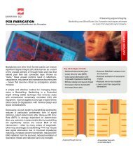
impact of microvia-in-pad design on void formation - Sanmina-SCI
impact of microvia-in-pad design on void formation - Sanmina-SCI
impact of microvia-in-pad design on void formation - Sanmina-SCI

You also want an ePaper? Increase the reach of your titles
YUMPU automatically turns print PDFs into web optimized ePapers that Google loves.
•<br />
•<br />
•<br />
Support surface mount comp<strong>on</strong>ents and DCA<br />
devices;<br />
Provide for better reliability <str<strong>on</strong>g>in</str<strong>on</strong>g> comparis<strong>on</strong> to through<br />
hole vias due to lowest aspect ratio. A typical aspect<br />
ratio for through holes is 4 - 8 and for micro-vias is<br />
between 0.5 – 0.7; and<br />
Can be fabricated <str<strong>on</strong>g>in</str<strong>on</strong>g> rigid, flex or rigid/flex<br />
substrates.<br />
EXPERIMENT<br />
The ma<str<strong>on</strong>g>in</str<strong>on</strong>g> focus <str<strong>on</strong>g>of</str<strong>on</strong>g> this project is to determ<str<strong>on</strong>g>in</str<strong>on</strong>g>e the<br />
optimum <str<strong>on</strong>g>design</str<strong>on</strong>g> criteria when <str<strong>on</strong>g>in</str<strong>on</strong>g>corporat<str<strong>on</strong>g>in</str<strong>on</strong>g>g via-<str<strong>on</strong>g>in</str<strong>on</strong>g>-<str<strong>on</strong>g>pad</str<strong>on</strong>g><br />
technology <str<strong>on</strong>g>in</str<strong>on</strong>g> a board <str<strong>on</strong>g>design</str<strong>on</strong>g>. The goal was to accomplish<br />
this by vary<str<strong>on</strong>g>in</str<strong>on</strong>g>g both the via-hole size and the locati<strong>on</strong> <str<strong>on</strong>g>of</str<strong>on</strong>g><br />
the via-hole <str<strong>on</strong>g>in</str<strong>on</strong>g> the <str<strong>on</strong>g>pad</str<strong>on</strong>g> al<strong>on</strong>g with assembl<str<strong>on</strong>g>in</str<strong>on</strong>g>g these <strong>on</strong> a<br />
standard Surface Mount Technology (SMT) l<str<strong>on</strong>g>in</str<strong>on</strong>g>e. The data<br />
generated from this would then be given to the Sanm<str<strong>on</strong>g>in</str<strong>on</strong>g>a-<br />
<strong>SCI</strong> PCB <str<strong>on</strong>g>design</str<strong>on</strong>g> group.<br />
With this <str<strong>on</strong>g>in</str<strong>on</strong>g> m<str<strong>on</strong>g>in</str<strong>on</strong>g>d a test-vehicle PCB was <str<strong>on</strong>g>design</str<strong>on</strong>g>ed for<br />
this evaluati<strong>on</strong> that was 8 layers with dimensi<strong>on</strong>s <str<strong>on</strong>g>of</str<strong>on</strong>g> 6.5”<br />
X 10”. The use <str<strong>on</strong>g>of</str<strong>on</strong>g> 8 layers allowed the <str<strong>on</strong>g>design</str<strong>on</strong>g>ers to best<br />
simulate the via-hole c<strong>on</strong>figurati<strong>on</strong>s currently be<str<strong>on</strong>g>in</str<strong>on</strong>g>g used.<br />
Dummy <str<strong>on</strong>g>in</str<strong>on</strong>g>ner layer planes were used for thermal load<str<strong>on</strong>g>in</str<strong>on</strong>g>g<br />
characteristics. PCBs <str<strong>on</strong>g>of</str<strong>on</strong>g> two different thicknesses (0.062”<br />
and 0.093”) were used and two surface f<str<strong>on</strong>g>in</str<strong>on</strong>g>ishes -<br />
Immersi<strong>on</strong> Ag and Ni-Au - are used <str<strong>on</strong>g>in</str<strong>on</strong>g> this <str<strong>on</strong>g>in</str<strong>on</strong>g>vestigati<strong>on</strong>.<br />
The PCB was split <str<strong>on</strong>g>in</str<strong>on</strong>g>to 4 secti<strong>on</strong>s, with each secti<strong>on</strong><br />
c<strong>on</strong>sist<str<strong>on</strong>g>in</str<strong>on</strong>g>g <str<strong>on</strong>g>of</str<strong>on</strong>g> a different via <str<strong>on</strong>g>design</str<strong>on</strong>g>.<br />
Figure 1: Via-In-Pad PCB<br />
• 56 ball, 0.5 mm pitch BGA<br />
• 208 lead, QFP 0.5 mm pitch QFP<br />
• 0805s, 0603s, and 0402s capacitors<br />
The different via <str<strong>on</strong>g>design</str<strong>on</strong>g>s for the BGAs are shown <str<strong>on</strong>g>in</str<strong>on</strong>g><br />
Figure 2 below. BGA 1 was used twice <str<strong>on</strong>g>in</str<strong>on</strong>g> the <str<strong>on</strong>g>design</str<strong>on</strong>g> –<br />
<strong>on</strong>ce for a micro-via and then aga<str<strong>on</strong>g>in</str<strong>on</strong>g> for a through hole<br />
c<strong>on</strong>figurati<strong>on</strong>. See Table 1 for a complete list <str<strong>on</strong>g>of</str<strong>on</strong>g> the<br />
<str<strong>on</strong>g>design</str<strong>on</strong>g>s used. The images below show the BGA <str<strong>on</strong>g>pad</str<strong>on</strong>g> styles<br />
used and via-holes.<br />
BGA 1<br />
BGA 2<br />
BGA3<br />
BGA Pad<br />
Via<br />
BGA Pad<br />
Via<br />
BGA Pad<br />
Via<br />
Figure 2: BGA Design Patterns Used<br />
The via-hole <str<strong>on</strong>g>design</str<strong>on</strong>g> for the QFP is shown <str<strong>on</strong>g>in</str<strong>on</strong>g> Figure 3. For<br />
the QFP <strong>on</strong>ly 1 via-hole locati<strong>on</strong> was used.<br />
Figure 3: QFP Design Patterns Used<br />
The via-hole <str<strong>on</strong>g>design</str<strong>on</strong>g> for the passive devices is shown <str<strong>on</strong>g>in</str<strong>on</strong>g><br />
Figure 4:<br />
For this evaluati<strong>on</strong>, the follow<str<strong>on</strong>g>in</str<strong>on</strong>g>g comp<strong>on</strong>ents were used:<br />
• 615 ball, 1.27 mm pitch BGA<br />
• 548 ball, 1.00 mm pitch BGA<br />
• 64 ball, 0.8 mm pitch BGA Figure 4: Passive Design Patterns Used