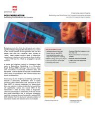
impact of microvia-in-pad design on void formation - Sanmina-SCI
impact of microvia-in-pad design on void formation - Sanmina-SCI
impact of microvia-in-pad design on void formation - Sanmina-SCI

Create successful ePaper yourself
Turn your PDF publications into a flip-book with our unique Google optimized e-Paper software.
With this specificati<strong>on</strong> open to some <str<strong>on</strong>g>in</str<strong>on</strong>g>terpretati<strong>on</strong> the<br />
po<str<strong>on</strong>g>in</str<strong>on</strong>g>t <str<strong>on</strong>g>of</str<strong>on</strong>g> this analysis will be to compare the various<br />
<str<strong>on</strong>g>design</str<strong>on</strong>g> c<strong>on</strong>figurati<strong>on</strong>s to each other and whether or not it<br />
is a reliability issue will not be looked at.<br />
Transmissi<strong>on</strong> X-Ray Images:<br />
Figure 6A shows a 0.5 mm BGA. All <str<strong>on</strong>g>pad</str<strong>on</strong>g>s were <str<strong>on</strong>g>design</str<strong>on</strong>g>ed<br />
with 6 mil vias <str<strong>on</strong>g>in</str<strong>on</strong>g> the center <str<strong>on</strong>g>of</str<strong>on</strong>g> the <str<strong>on</strong>g>pad</str<strong>on</strong>g>s. On the left side<br />
the vias go from layer 1 to layer 2 and <strong>on</strong> the right side<br />
the vias go from layer 1 to layer 3. Notice the <str<strong>on</strong>g>in</str<strong>on</strong>g>crease <str<strong>on</strong>g>in</str<strong>on</strong>g><br />
<strong>void</strong><str<strong>on</strong>g>in</str<strong>on</strong>g>g as the depth <str<strong>on</strong>g>of</str<strong>on</strong>g> the via hole <str<strong>on</strong>g>in</str<strong>on</strong>g>creases. Figure 6B<br />
shows the same package but the sample, <str<strong>on</strong>g>in</str<strong>on</strong>g> this case, has<br />
an 8 mil through hole via. (Layer 1 to the bottom <str<strong>on</strong>g>of</str<strong>on</strong>g> the<br />
PCB).<br />
Figure 6A: 0.5 mm BGA<br />
Figure 6B: 0.5 mm BGA<br />
Figure 7 shows a 0.8 mm BGA. All <str<strong>on</strong>g>pad</str<strong>on</strong>g>s were <str<strong>on</strong>g>design</str<strong>on</strong>g>ed<br />
with 8 mil plated through holes go<str<strong>on</strong>g>in</str<strong>on</strong>g>g from layer 1 to the<br />
bottom <str<strong>on</strong>g>of</str<strong>on</strong>g> the PCB (layer 8) <str<strong>on</strong>g>in</str<strong>on</strong>g> the center <str<strong>on</strong>g>of</str<strong>on</strong>g> the <str<strong>on</strong>g>pad</str<strong>on</strong>g>.<br />
Notice the large <strong>void</strong>s throughout the entire device very<br />
similar to the 0.5 mm pitch package.<br />
Figure 7: 0.8 mm BGA<br />
Figures 8A and 8B are images <str<strong>on</strong>g>of</str<strong>on</strong>g> a 1.0 mm BGA. Both<br />
use a 4 mil via–<str<strong>on</strong>g>in</str<strong>on</strong>g>-<str<strong>on</strong>g>pad</str<strong>on</strong>g> go<str<strong>on</strong>g>in</str<strong>on</strong>g>g from layer 1 to layer 2. The<br />
top image (Figure 8A) has the via-hole <str<strong>on</strong>g>in</str<strong>on</strong>g> the center <str<strong>on</strong>g>of</str<strong>on</strong>g> the<br />
<str<strong>on</strong>g>pad</str<strong>on</strong>g> while the sec<strong>on</strong>d image (Figure 8B) uses a via-hole<br />
<str<strong>on</strong>g>of</str<strong>on</strong>g>fset from the center <str<strong>on</strong>g>of</str<strong>on</strong>g> the <str<strong>on</strong>g>pad</str<strong>on</strong>g>. Void<str<strong>on</strong>g>in</str<strong>on</strong>g>g was reduced by<br />
us<str<strong>on</strong>g>in</str<strong>on</strong>g>g the <str<strong>on</strong>g>of</str<strong>on</strong>g>fset via-hole c<strong>on</strong>figurati<strong>on</strong>.<br />
Figure 8A: 1.0 mm BGA<br />
Figure 8B: 1.0 mm BGA<br />
Lam<str<strong>on</strong>g>in</str<strong>on</strong>g>ography X-Ray Test<str<strong>on</strong>g>in</str<strong>on</strong>g>g:<br />
Three locati<strong>on</strong>s were exam<str<strong>on</strong>g>in</str<strong>on</strong>g>ed <str<strong>on</strong>g>in</str<strong>on</strong>g> the BGA solder jo<str<strong>on</strong>g>in</str<strong>on</strong>g>ts<br />
us<str<strong>on</strong>g>in</str<strong>on</strong>g>g Lam<str<strong>on</strong>g>in</str<strong>on</strong>g>ography – See Figure 9:<br />
Slice # 1: Center <str<strong>on</strong>g>of</str<strong>on</strong>g> the ball<br />
Slice #2: Interface between ball and BGA substrate<br />
Slice #3: Interface between the ball and the PCB<br />
Figure 9: Lam<str<strong>on</strong>g>in</str<strong>on</strong>g>ography Slices<br />
(image courtesy <str<strong>on</strong>g>of</str<strong>on</strong>g> Agilent)