Download - Nanowerk
Download - Nanowerk
Download - Nanowerk

Create successful ePaper yourself
Turn your PDF publications into a flip-book with our unique Google optimized e-Paper software.
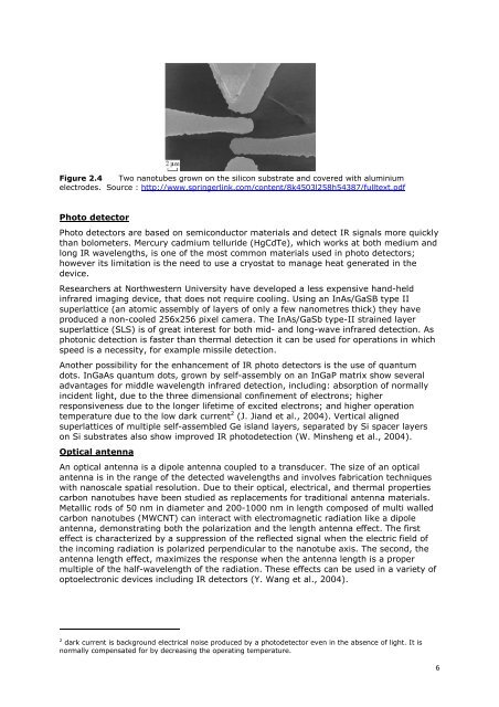
Figure 2.4 Two nanotubes grown on the silicon substrate and covered with aluminium<br />
electrodes. Source : http://www.springerlink.com/content/8k4503l258h54387/fulltext.pdf<br />
Photo detector<br />
Photo detectors are based on semiconductor materials and detect IR signals more quickly<br />
than bolometers. Mercury cadmium telluride (HgCdTe), which works at both medium and<br />
long IR wavelengths, is one of the most common materials used in photo detectors;<br />
however its limitation is the need to use a cryostat to manage heat generated in the<br />
device.<br />
Researchers at Northwestern University have developed a less expensive hand-held<br />
infrared imaging device, that does not require cooling. Using an InAs/GaSB type II<br />
superlattice (an atomic assembly of layers of only a few nanometres thick) they have<br />
produced a non-cooled 256x256 pixel camera. The InAs/GaSb type-II strained layer<br />
superlattice (SLS) is of great interest for both mid- and long-wave infrared detection. As<br />
photonic detection is faster than thermal detection it can be used for operations in which<br />
speed is a necessity, for example missile detection.<br />
Another possibility for the enhancement of IR photo detectors is the use of quantum<br />
dots. InGaAs quantum dots, grown by self-assembly on an InGaP matrix show several<br />
advantages for middle wavelength infrared detection, including: absorption of normally<br />
incident light, due to the three dimensional confinement of electrons; higher<br />
responsiveness due to the longer lifetime of excited electrons; and higher operation<br />
temperature due to the low dark current 2 (J. Jiand et al., 2004). Vertical aligned<br />
superlattices of multiple self-assembled Ge island layers, separated by Si spacer layers<br />
on Si substrates also show improved IR photodetection (W. Minsheng et al., 2004).<br />
Optical antenna<br />
An optical antenna is a dipole antenna coupled to a transducer. The size of an optical<br />
antenna is in the range of the detected wavelengths and involves fabrication techniques<br />
with nanoscale spatial resolution. Due to their optical, electrical, and thermal properties<br />
carbon nanotubes have been studied as replacements for traditional antenna materials.<br />
Metallic rods of 50 nm in diameter and 200-1000 nm in length composed of multi walled<br />
carbon nanotubes (MWCNT) can interact with electromagnetic radiation like a dipole<br />
antenna, demonstrating both the polarization and the length antenna effect. The first<br />
effect is characterized by a suppression of the reflected signal when the electric field of<br />
the incoming radiation is polarized perpendicular to the nanotube axis. The second, the<br />
antenna length effect, maximizes the response when the antenna length is a proper<br />
multiple of the half-wavelength of the radiation. These effects can be used in a variety of<br />
optoelectronic devices including IR detectors (Y. Wang et al., 2004).<br />
2 dark current is background electrical noise produced by a photodetector even in the absence of light. It is<br />
normally compensated for by decreasing the operating temperature.<br />
6